
Technical Data
DSP56L307/D
Rev. 3, 4/2003
24-Bit Digital Signal
Processor
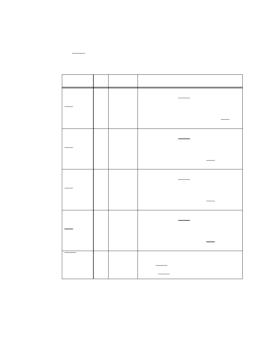
Figure 1. DSP56L307 Block Diagram
YAB
XAB
PAB
YDB
XDB
PDB
GDB
MODB/IRQB
MODC/IRQC
13
MODD/IRQD
DSP56300
6
16
24-Bit
24
18
DDB
DAB
Peripheral
Core
YM
_
E
B
XM
_
E
B
PM
_
E
B
PI
O
_
EB
Expansion Area
6
5
3
RESET
MODA/IRQA
PINIT/NMI
EXTAL
XTAL
Address
Control
Data
Address
Generation
Unit
Six Channel
DMA Unit
Program
Interrupt
Controller
Program
Decode
Controller
Program
Address
Generator
Data ALU
24
◊
24 + 56
56-bit MAC
Two 56-bit Accumulators
56-bit Barrel Shifter
Power
Management
External
Bus
Interface
and
I - Cache
Control
Memory Expansion Area
DE
Program
RAM
16 K
◊
24 bits
X Data
RAM
24 K
◊
24 bits
Y Data
RAM
24 K
◊
24 bits
External
Address
Bus
Switch
SCI
EFCOP
ESSI
HI08
Triple
Timer
or
15 K
◊
24 bits
Instruction
Cache
1024
◊
24 bits
Bootstrap
ROM
PCAP
and
OnCETM
JTAG
PLL
Clock
Generator
Internal
Data
Bus
Switch
External
Data
Bus
Switch
The DSP56L307 is
intended for
applications requiring
a large amount of
on-chip memory, such
as networking and
wireless infrastructure
applications. The
EFCOP can accelerate
general filtering
applications, such as
echo-cancellation
applications,
correlation, and
general-purpose
convolution-based
algorithms.
The Motorola DSP56L307, a member of the
DSP56300 Digital Signal Processor (DSP) family,
supports network applications with general
filtering operations. The Enhanced Filter
Coprocessor (EFCOP) executes filter algorithms in
parallel with core operations, enhancing signal
quality with no impact on channel throughput or
total channels supported. The result is increased
overall performance. Like the other DSP56300
family members, the DSP56L307 uses a
high-performance, single-clock-cycle-per-
instruction engine (DSP56000 code-compatible), a
barrel shifter, 24-bit addressing, an instruction
cache, and a direct memory access (DMA)
controller (see Figure 1). The DSP56L307
performs at 160 million instructions per second
(MIPS), attaining 290 MIPS when the EFCOP is in
use. It operates with an internal 160 MHz clock
with a 1.8 volt core and independent 3.3 volt
input/output (I/O) power.
Advance Information
Note: This document contains information on a new product. Specifications and information herein are subject to change without notice.

ii
Table of Contents
DSP56L307 Features ......................................................................................................................................... iii
Target Applications ..............................................................................................................................................v
Product Documentation........................................................................................................................................v
Chapter 1
Signal/ Connection Descriptions
1.1
Signal Groupings.............................................................................................................................................. 1-1
1.2
Power................................................................................................................................................................ 1-3
1.3
Ground.............................................................................................................................................................. 1-3
1.4
Clock ................................................................................................................................................................ 1-4
1.5
PLL................................................................................................................................................................... 1-4
1.6
External Memory Expansion Port (Port A)...................................................................................................... 1-5
1.7
Interrupt and Mode Control ............................................................................................................................. 1-8
1.8
Host Interface (HI08) ....................................................................................................................................... 1-9
1.9
Enhanced Synchronous Serial Interface 0 (ESSI0)........................................................................................ 1-13
1.10
Enhanced Synchronous Serial Interface 1 (ESSI1)........................................................................................ 1-14
1.11
Serial Communication Interface (SCI)........................................................................................................... 1-16
1.12
Timers............................................................................................................................................................. 1-17
1.13
JTAG and OnCE Interface ............................................................................................................................. 1-18
Chapter 2
Specifications
2.1
Introduction ...................................................................................................................................................... 2-1
2.2
Maximum Ratings ............................................................................................................................................ 2-1
2.3
Thermal Characteristics ................................................................................................................................... 2-2
2.4
DC Electrical Characteristics ........................................................................................................................... 2-3
2.5
AC Electrical Characteristics ........................................................................................................................... 2-4
Chapter 3
Packaging
3.1
Pin-Out and Package Information .................................................................................................................... 3-1
3.2
MAP-BGA Package Description ..................................................................................................................... 3-2
3.3
MAP-BGA Package Mechanical Drawing .................................................................................................... 3-10
Chapter 4
Design Considerations
4.1
Thermal Design Considerations ....................................................................................................................... 4-1
4.2
Electrical Design Considerations ..................................................................................................................... 4-2
4.3
Power Consumption Considerations ................................................................................................................ 4-4
4.4
PLL Performance Issues .................................................................................................................................. 4-5
4.5
Input (EXTAL) Jitter Requirements................................................................................................................. 4-5
Appendix A
Power Consumption Benchmark
Index
Data Sheet Conventions
OVERBAR
Used to indicate a signal that is active when pulled low (For example, the RESET pin is active when
low.)
"asserted"
Means that a high true (active high) signal is high or that a low true (active low) signal is low
"deasserted"
Means that a high true (active high) signal is low or that a low true (active low) signal is high
Examples:
Signal/Symbol
Logic State
Signal State
Voltage
PIN
True
Asserted
V
IL
/V
OL
PIN
False
Deasserted
V
IH
/V
OH
PIN
True
Asserted
V
IH
/V
OH
PIN
False
Deasserted
V
IL
/V
OL
Note: Values for V
IL
, V
OL
, V
IH
, and V
OH
are defined by individual product specifications.

iii
DSP56L307 Features
High-Performance DSP56300 Core
∑ 160 million instructions per second (MIPS) (290 MIPS using the EFCOP in filtering applications) with
a 160 MHz clock at 1.8 V core and 3.3 V I/O
∑ Object code compatible with the DSP56000 core with highly parallel instruction set
∑ Data Arithmetic Logic Unit (Data ALU) with fully pipelined 24
◊
24-bit parallel
Multiplier-Accumulator (MAC), 56-bit parallel barrel shifter (fast shift and normalization; bit stream
generation and parsing), conditional ALU instructions, and 24-bit or 16-bit arithmetic support under
software control
∑ Program Control Unit (PCU) with Position Independent Code (PIC) support, addressing modes
optimized for DSP applications (including immediate offsets), on-chip instruction cache controller,
on-chip memory-expandable hardware stack, nested hardware DO loops, and fast auto-return interrupts
∑ Direct Memory Access (DMA) with six DMA channels supporting internal and external accesses;
one-, two-, and three-dimensional transfers (including circular buffering); end-of-block-transfer
interrupts; and triggering from interrupt lines and all peripherals
∑ Phase Lock Loop (PLL) allows change of low-power Divide Factor (DF) without loss of lock and
output clock with skew elimination
∑ Hardware debugging support including On-Chip Emulation (OnCE
) module, Joint Test Action
Group (JTAG) Test Access Port (TAP)
Enhanced Filtering Coprocessor (EFCOP)
∑ On-chip 24
◊
24-bit filtering and echo-cancellation coprocessor that runs in parallel to the DSP core
∑ Operation at the same frequency as the core (up to 160 MHz)
∑ Support for a variety of filter modes, some of which are optimized for cellular base station applications:
-- Real Finite Impulse Response (FIR) with real taps
-- Complex FIR with complex taps
-- Complex FIR generating pure real or pure imaginary outputs alternately
-- A 4-bit decimation factor in FIR filters, thus providing a decimation ratio up to 16
-- Direct form 1 (DFI) Infinite Impulse Response (IIR) filter
-- Direct form 2 (DFII) IIR filter
-- Four scaling factors (1, 4, 8, 16) for IIR output
-- Adaptive FIR filter with true least mean square (LMS) coefficient updates
-- Adaptive FIR filter with delayed LMS coefficient updates
On-Chip Peripherals
∑ Enhanced DSP56000-like 8-bit parallel host interface (HI08) supports a variety of buses (for example,
ISA) and provides glueless connection to a number of industry-standard microcomputers,
microprocessors, and DSPs
∑ Two enhanced synchronous serial interfaces (ESSI), each with one receiver and three transmitters
(allows six-channel home theater)
∑ Serial communications interface (SCI) with baud rate generator
∑ Triple timer module
∑ Up to 34 programmable general-purpose input/output (GPIO) pins, depending on which peripherals are
enabled

iv
On-Chip Memories
∑ 192
◊
24-bit bootstrap ROM
∑ 64 K RAM total
∑ Program RAM, Instruction Cache, X data RAM, and Y data RAM sizes are programmable:
Off-Chip Memory Expansion
∑ Data memory expansion to two 256 K
◊
24-bit word memory spaces using the standard external
address lines
∑ Program memory expansion to one 256 K
◊
24-bit words memory space using the standard external
address lines
∑ External memory expansion port
∑ Chip Select Logic for glueless interface to static random access memory (SRAMs)
∑ On-chip DRAM Controller for glueless interface to dynamic random access memory (DRAMs) up to
100 MHz operating frequency
Reduced Power Dissipation
∑ Very low-power CMOS design
∑ Wait and Stop low-power standby modes
∑ Fully static design specified to operate down to 0 Hz (dc)
∑ Optimized power management circuitry (instruction-dependent, peripheral-dependent, and
mode-dependent)
Packaging
The DSP56L307 is available in a 196-pin MAP-BGA package.
Program
RAM Size
Instruction
Cache Size
X Data RAM Size* Y Data RAM Size*
Instruction
Cache
Switch
Mode
MSW1
MSW0
16 K
◊
24-bit
0
24 K
◊
24-bit
24 K
◊
24-bit
disabled
disabled
0/1
0/1
15 K
◊
24-bit
1024
◊
24-bit
24 K
◊
24-bit
24 K
◊
24-bit
enabled
disabled
0/1
0/1
48 K
◊
24-bit
0
8 K
◊
24-bit
8 K
◊
24-bit
disabled
enabled
0
0
47 K
◊
24-bit
1024
◊
24-bit
8 K
◊
24-bit
8 K
◊
24-bit
enabled
enabled
0
0
40 K
◊
24-bit
0
12 K
◊
24-bit
12 K
◊
24-bit
disabled
enabled
0
1
39 K
◊
24-bit
1024
◊
24-bit
12 K
◊
24-bit
12 K
◊
24-bit
enabled
enabled
0
1
32 K
◊
24-bit
0
16 K
◊
24-bit
16 K
◊
24-bit
disabled
enabled
1
0
31 K
◊
24-bit
1024
◊
24-bit
16 K
◊
24-bit
16 K
◊
24-bit
enabled
enabled
1
0
24 K
◊
24-bit
0
20 K
◊
24-bit
20 K
◊
24-bit
disabled
enabled
1
1
23 K
◊
24-bit
1024
◊
24-bit
20 K
◊
24-bit
20 K
◊
24-bit
enabled
enabled
1
1
*Includes 4 K
◊
24-bit shared memory (that is, memory shared by the core and the EFCOP)
v
Target Applications
∑ Wireless and wireline infrastructure applications
∑ Multi-channel wireless local loop systems
∑ DSP resource boards
∑ High-speed modem banks
∑ Packet telephony
Product Documentation
The three documents listed in the following table are required for a complete description of the
DSP56L307 and are necessary to design properly with the part. Documentation is available from the
following sources. (See the back cover for details.)
∑ A local Motorola distributor
∑ A Motorola semiconductor sales office
∑ A Motorola Literature Distribution Center
∑ The World Wide Web (WWW)
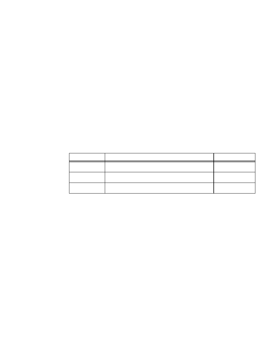
Table 1. DSP56L307 Documentation
Name
Description
Order Number
DSP56300 Family
Manual
Detailed description of the DSP56300 family processor core and
instruction set
DSP56300FM/AD
DSP56L307 User's
Manual
Detailed functional description of the DSP56L307 memory
configuration, operation, and register programming
DSP56L307UM/D
DSP56L307
Technical Data
DSP56L307 features list and physical, electrical, timing, and
package specifications
DSP56L307/D

vi

1-1
Chapter 1
Signal/
Connection
Descriptions
1.1 Signal Groupings
The DSP56L307 input and output signals are organized into functional groups as shown in Table 1-1.
Figure 1-1 diagrams the DSP56L307 signals by functional group. The remainder of this chapter
describes the signal pins in each functional group.
Note:
This chapter refers to a number of configuration registers used to select individual multiplexed
signal functionality. Refer to the
DSP56L307
User's Manual for details on these configuration
registers.
Table 1-1. DSP56L307 Functional Signal Groupings
Functional Group
Number
of
Signals
Power (V
CC
)
20
Ground (GND)
66
Clock
2
PLL
3
Address bus
Port A
1
18
Data bus
24
Bus control
13
Interrupt and mode control
5
Host interface (HI08)
Port B
2
16
Enhanced synchronous serial interface (ESSI)
Ports C and D
3
12
Serial communication interface (SCI)
Port E
4
3
Timer
3
OnCE/JTAG Port
6
Notes:
1.
Port A signals define the external memory interface port, including the external address bus, data
bus, and control signals. The Clock Output (CLKOUT), BCLK, BCLK, CAS, and RAS[0≠3] signals
used by other DSP56300 family members are supported by the DSP56L307 at operating frequencies
up to 100 MHz. DRAM access is not supported above 100 MHz.
2.
Port B signals are the HI08 port signals multiplexed with the GPIO signals.
3.
Port C and D signals are the two ESSI port signals multiplexed with the GPIO signals.
4.
Port E signals are the SCI port signals multiplexed with the GPIO signals.
5.
There are 5 signal connections that are not used. These are designated as no connect (NC) in the
package description (see Chapter 3).
1-2
Signal Groupings
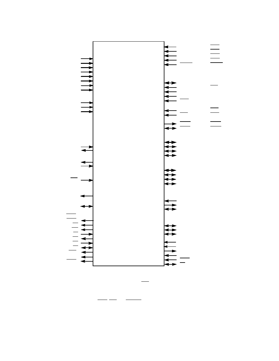
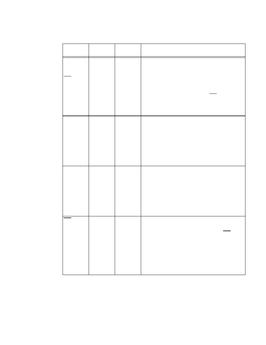
Figure 1-1. Signals Identified by Functional Group
Notes:
1.
The HI08 port supports a non-multiplexed or a multiplexed bus, single or double Data Strobe (DS), and single or
double Host Request (HR) configurations. Since each of these modes is configured independently, any combination
of these modes is possible. These HI08 signals can also be configured alternatively as GPIO signals (PB[0≠15]).
Signals with dual designations (for example, HAS/HAS) have configurable polarity.
2.
The ESSI0, ESSI1, and SCI signals are multiplexed with the Port C GPIO signals (PC[0≠5]), Port D GPIO signals
(PD[0≠5]), and Port E GPIO signals (PE[0≠2]), respectively.
3.
TIO[0≠2] can be configured as GPIO signals.
4.
CLKOUT, BCLK, BCLK, CAS, and RAS[0≠3] are valid only for operating frequencies
100 MHz.
DSP56L307
24
18
External
Address Bus
External
Data Bus
External
Bus
Control
Enhanced
Synchronous Serial
Interface Port 0
(ESSI0)
2
Timers
3
PLL
OnCE/
JTAG Port
Power Inputs:
PLL
Core Logic
I/O
Address Bus
Data Bus
Bus Control
HI08
ESSI/SCI/Timer
A[0≠17]
D[0≠23]
AA0/RAS0≠
AA3/RAS3
4
RD
WR
TA
BR
BG
BB
CAS
4
BCLK
4
BCLK
4
TCK
TDI
TDO
TMS
TRST
DE
CLKOUT
4
PCAP
After
Reset
NMI
V
CCP
V
CCQL
V
CCQH
V
CCA
V
CCD
V
CCC
V
CCH
V
CCS
4
Serial
Communications
Interface (SCI) Port
2
4
2
2
Grounds:
PLL
PLL
Ground plane
GND
P
GND
P1
GND
64
Interrupt/
Mode Control
MODA
MODB
MODC
MODD
RESET
Host
Interface
(HI08) Port
1
Non-Multiplexed
Bus
H[0≠7]
HA0
HA1
HA2
HCS/HCS
Single DS
HRW
HDS/HDS
Single HR
HREQ/HREQ
HACK/HACK
RXD
TXD
SCLK
SC0[0≠2]
SCK0
SRD0
STD0
TIO0
TIO1
TIO2
8
3
3
EXTAL
XTAL
Clock
Enhanced
Synchronous Serial
Interface Port 1
(ESSI1)
2
SC1[0≠2]
SCK1
SRD1
STD1
3
Multiplexed
Bus
HAD[0≠7]
HAS/HAS
HA8
HA9
HA10
Double DS
HRD/HRD
HWR/HWR
Double HR
HTRQ/HTRQ
HRRQ/HRRQ
Port B
GPIO
PB[0≠7]
PB8
PB9
PB10
PB13
PB11
PB12
PB14
PB15
Port E GPIO
PE0
PE1
PE2
Port C GPIO
PC[0≠2]
PC3
PC4
PC5
Port D GPIO
PD[0≠2]
PD3
PD4
PD5
Timer GPIO
TIO0
TIO1
TIO2
Port A
4
IRQA
IRQB
IRQC
IRQD
PINIT
3
RESET
During Reset
After Reset
Reset
During
1-3
Power
1.2 Power
1.3 Ground
Table 1-2. Power Inputs
Power Name
Description
V
CCP
PLL Power--V
CC
dedicated for PLL use. The voltage should be well-regulated and the input
should be provided with an extremely low impedance path to the V
CC
power rail.
V
CCQL
Quiet Core (Low) Power--An isolated power for the core processing logic. This input must
be isolated externally from all other chip power inputs.
V
CCQH
Quiet External (High) Power--A quiet power source for I/O lines. This input must be tied
externally to all other chip power inputs, except V
CCQL
.
V
CCA
Address Bus Power--An isolated power for sections of the address bus I/O drivers. This
input must be tied externally to all other chip power inputs, except V
CCQL
.
V
CCD
Data Bus Power--An isolated power for sections of the data bus I/O drivers. This input must
be tied externally to all other chip power inputs, except V
CCQL
.
V
CCC
Bus Control Power--An isolated power for the bus control I/O drivers. This input must be
tied externally to all other chip power inputs, except V
CCQL
.
V
CCH
Host Power--An isolated power for the HI08 I/O drivers. This input must be tied externally to
all other chip power inputs, except V
CCQL
.
V
CCS
ESSI, SCI, and Timer Power--An isolated power for the ESSI, SCI, and timer I/O drivers.
This input must be tied externally to all other chip power inputs, except V
CCQL
.
Note: The user must provide adequate external decoupling capacitors for all power connections.
Table 1-3. Grounds
Ground
Name
Description
GND
P
PLL Ground--Ground-dedicated for PLL use. The connection should be provided with an extremely
low-impedance path to ground. V
CCP
should be bypassed to GND
P
by a 0.47
µ
F capacitor located as
close as possible to the chip package.
GND
P1
PLL Ground 1--Ground-dedicated for PLL use. The connection should be provided with an extremely
low-impedance path to ground.
GND
Ground--Connected to an internal device ground plane.
Note: The user must provide adequate external decoupling capacitors for all GND connections.
1-4
Clock
1.4 Clock
1.5 PLL
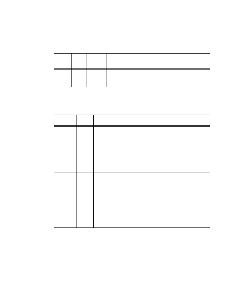
Table 1-4. Clock Signals
Signal
Name
Type
State
During
Reset
Signal Description
EXTAL
Input
Input
External Clock/Crystal Input--Interfaces the internal crystal oscillator
input to an external crystal or an external clock.
XTAL
Output
Chip-driven
Crystal Output--Connects the internal crystal oscillator output to an
external crystal. If an external clock is used, leave XTAL unconnected.
Table 1-5. Phase-Locked Loop Signals
Signal
Name
Type
State During
Reset
Signal Description
CLKOUT
Output
Chip-driven
Clock Output--Provides an output clock synchronized to the
internal core clock phase.
If the PLL is enabled and both the multiplication and division
factors equal one, then CLKOUT is also synchronized to EXTAL.
If the PLL is disabled, the CLKOUT frequency is half the
frequency of EXTAL.
Note: At operating frequencies above 100 MHz, this signal
produces a low-amplitude waveform that is not usable externally
by other devices.
PCAP
Input
Input
PLL Capacitor--An input connecting an off-chip capacitor to the
PLL filter. Connect one capacitor terminal to PCAP and the other
terminal to V
CCP
.
If the PLL is not used, PCAP can be tied to V
CC
, GND, or left
floating.
PINIT
NMI
Input
Input
Input
PLL Initial--During assertion of RESET, the value of PINIT is
written into the PLL enable (PEN) bit of the PLL control (PCTL)
register, determining whether the PLL is enabled or disabled.
Nonmaskable Interrupt--After RESET deassertion and during
normal instruction processing, this Schmitt-trigger input is the
negative-edge-triggered NMI request internally synchronized to
CLKOUT.

1-5
External Memory Expansion Port (Port A)
1.6 External Memory Expansion Port (Port A)
Note:
When the DSP56L307 enters a low-power standby mode (stop or wait), it releases bus
mastership and tri-states the relevant Port A signals:
A[0≠17]
,
D[0≠23]
,
AA0/RAS0
≠
AA3/RAS3
,
RD
,
WR
,
BB
,
CAS
.
1.6.1 External Address Bus
1.6.2 External Data Bus
Table 1-6. External Address Bus Signals
Signal
Name
Type
State During
Reset, Stop, or
Wait
Signal Description
A[0≠17]
Output
Tri-stated
Address Bus--When the DSP is the bus master, A[0≠17] are
active-high outputs that specify the address for external
program and data memory accesses. Otherwise, the signals
are tri-stated. To minimize power dissipation, A[0≠17] do not
change state when external memory spaces are not being
accessed.
Table 1-7. External Data Bus Signals
Signal
Name
Type
State
During
Reset
State
During
Stop or
Wait
Signal Description
D[0≠23]
Input/ Output
Ignored
Input
Last state:
Input:
Ignored
Output:
Last value
Data Bus--When the DSP is the bus master, D[0≠23] are
active-high, bidirectional input/outputs that provide the
bidirectional data bus for external program and data memory
accesses. Otherwise, D[0≠23] drivers are tri-stated. If the last
state is output, these lines have weak keepers that maintain
the last output state even when all drivers are tri-stated.

1-6
External Memory Expansion Port (Port A)
1.6.3 External Bus Control
Table 1-8. External Bus Control Signals
Signal
Name
Type
State During
Reset, Stop, or
Wait
Signal Description
AA[0≠3]
RAS[0≠3]
Output
Output
Tri-stated
Address Attribute--When defined as AA, these signals can be used as
chip selects or additional address lines. The default use defines a
priority scheme under which only one AA signal can be asserted at a
time. Setting the AA priority disable (APD) bit (Bit 14) of the Operating
Mode Register, the priority mechanism is disabled and the lines can be
used together as four external lines that can be decoded externally into
16 chip select signals.
Row Address Strobe--When defined as RAS, these signals can be
used as RAS for DRAM interface. These signals are tri-statable outputs
with programmable polarity.
Note: DRAM access is not supported above 100 MHz.
RD
Output
Tri-stated
Read Enable--When the DSP is the bus master, RD is an active-low
output that is asserted to read external memory on the data bus
(D[0≠23]). Otherwise, RD is tri-stated.
WR
Output
Tri-stated
Write Enable--When the DSP is the bus master, WR is an active-low
output that is asserted to write external memory on the data bus
(D[0≠23]). Otherwise, the signals are tri-stated.
TA
Input
Ignored Input
Transfer Acknowledge--If the DSP56L307 is the bus master and there
is no external bus activity, or the DSP56L307 is not the bus master, the
TA input is ignored. The TA input is a data transfer acknowledge
(DTACK) function that can extend an external bus cycle indefinitely. Any
number of wait states (1, 2. . .infinity) can be added to the wait states
inserted by the bus control register (BCR) by keeping TA deasserted. In
typical operation, TA is deasserted at the start of a bus cycle, asserted
to enable completion of the bus cycle, and deasserted before the next
bus cycle. The current bus cycle completes one clock period after TA is
deasserted. The number of wait states is determined by the TA input or
by the BCR, whichever is longer. The BCR sets the minimum number of
wait states in external bus cycles. In order to use the TA functionality,
the BCR must be programmed to at least one wait state. A zero wait
state access cannot be extended by TA deassertion.
At operating frequencies
100 MHz, TA can operate synchronously
(with respect to CLKOUT) or asynchronously depending on the setting
of the TAS bit in the Operating Mode Register (OMR). If synchronous
mode is selected, the user is responsible for ensuring that TA transitions
occur synchronous to CLKOUT to ensure correct operation.
Synchronous operation is not supported above 100 MHz and the
OMR[TAS] bit must be set to synchronize the TA signal with the internal
clock.

1-7
External Memory Expansion Port (Port A)
BR
Output
Reset: Output
(deasserted)
State during
Stop/Wait depends
on BRH bit setting:
∑ BRH = 0: Output,
deasserted
∑ BRH = 1: Maintains
last state (that is, if
asserted, remains
asserted)
Bus Request--Asserted when the DSP requests bus mastership. BR is
deasserted when the DSP no longer needs the bus. BR may be
asserted or deasserted independently of whether the DSP56L307 is a
bus master or a bus slave. Bus "parking" allows BR to be deasserted
even though the DSP56L307 is the bus master. (See the description of
bus "parking" in the BB signal description.) The bus request hold (BRH)
bit in the BCR allows BR to be asserted under software control even
though the DSP does not need the bus. BR is typically sent to an
external bus arbitrator that controls the priority, parking, and tenure of
each master on the same external bus. BR is affected only by DSP
requests for the external bus, never for the internal bus. During
hardware reset, BR is deasserted and the arbitration is reset to the bus
slave state.
BG
Input
Ignored Input
Bus Grant--Asserted by an external bus arbitration circuit when the
DSP56L307 becomes the next bus master. When BG is asserted, the
DSP56L307 must wait until BB is deasserted before taking bus
mastership. When BG is deasserted, bus mastership is typically given
up at the end of the current bus cycle. This may occur in the middle of an
instruction that requires more than one external bus cycle for execution.
To ensure proper operation, the user must set the asynchronous bus
arbitration enable (ABE) bit (Bit 13) in the Operating Mode Register.
When this bit is set, BG and BB are synchronized internally. This adds a
required delay between the deassertion of an initial BG input and the
assertion of a subsequent BG input.
BB
Input/
Output
Ignored Input
Bus Busy--Indicates that the bus is active. Only after BB is deasserted
can the pending bus master become the bus master (and then assert
the signal again). The bus master may keep BB asserted after ceasing
bus activity regardless of whether BR is asserted or deasserted. Called
"bus parking," this allows the current bus master to reuse the bus
without rearbitration until another device requires the bus. BB is
deasserted by an "active pull-up" method (that is, BB is driven high and
then released and held high by an external pull-up resistor).
Notes:
1.
See BG for additional information.
2.
BB requires an external pull-up resistor.
CAS
Output
Tri-stated
Column Address Strobe--When the DSP is the bus master, CAS is an
active-low output used by DRAM to strobe the column address.
Otherwise, if the Bus Mastership Enable (BME) bit in the DRAM control
register is cleared, the signal is tri-stated.
Note: DRAM access is not supported above 100 MHz.
BCLK
Output
Tri-stated
Bus Clock
When the DSP is the bus master, BCLK is active when the address
trace enable (ATE) bit in the Operating Mode Register is set. When
BCLK is active and synchronized to CLKOUT by the internal PLL, BCLK
precedes CLKOUT by one-fourth of a clock cycle.
Note: At operating frequencies above 100 MHz, this signal produces a
low-amplitude waveform that is not usable externally by other devices.
BCLK
Output
Tri-stated
Bus Clock Not
When the DSP is the bus master, BCLK is the inverse of the BCLK
signal. Otherwise, the signal is tri-stated.
Note: At operating frequencies above 100 MHz, this signal produces a
low-amplitude waveform that is not usable externally by other devices.
Table 1-8. External Bus Control Signals (Continued)
Signal
Name
Type
State During
Reset, Stop, or
Wait
Signal Description
1-8
Interrupt and Mode Control
1.7 Interrupt and Mode Control
The interrupt and mode control signals select the chip operating mode as it comes out of hardware reset.
After
RESET
is deasserted, these inputs are hardware interrupt request lines.
Table 1-9. Interrupt and Mode Control
Signal Name
Type
State During
Reset
Signal Description
MODA
IRQA
Input
Input
Schmitt-trigger
Input
Mode Select A--MODA, MODB, MODC, and MODD select one
of 16 initial chip operating modes, latched into the Operating
Mode Register when the RESET signal is deasserted.
External Interrupt Request A--After reset, this input becomes a
level-sensitive or negative-edge-triggered, maskable interrupt
request input during normal instruction processing. If the
processor is in the STOP or WAIT standby state and IRQA is
asserted, the processor exits the STOP or WAIT state.
MODB
IRQB
Input
Input
Schmitt-trigger
Input
Mode Select B--MODA, MODB, MODC, and MODD select one
of 16 initial chip operating modes, latched into the Operating
Mode Register when the RESET signal is deasserted.
External Interrupt Request B--After reset, this input becomes a
level-sensitive or negative-edge-triggered, maskable interrupt
request input during normal instruction processing. If the
processor is in the WAIT standby state and IRQB is asserted, the
processor exits the WAIT state.
MODC
IRQC
Input
Input
Schmitt-trigger
Input
Mode Select C--MODA, MODB, MODC, and MODD select one
of 16 initial chip operating modes, latched into the Operating
Mode Register when the RESET signal is deasserted.
External Interrupt Request C--After reset, this input becomes a
level-sensitive or negative-edge-triggered, maskable interrupt
request input during normal instruction processing. If the
processor is in the WAIT standby state and IRQC is asserted, the
processor exits the WAIT state.
MODD
IRQD
Input
Input
Schmitt-trigger
Input
Mode Select D--MODA, MODB, MODC, and MODD select one
of 16 initial chip operating modes, latched into the Operating
Mode Register when the RESET signal is deasserted.
External Interrupt Request D--After reset, this input becomes a
level-sensitive or negative-edge-triggered, maskable interrupt
request input during normal instruction processing. If the
processor is in the WAIT standby state and IRQD is asserted, the
processor exits the WAIT state.
RESET
Input
Schmitt-trigger
Input
Reset--Places the chip in the Reset state and resets the internal
phase generator. The Schmitt-trigger input allows a slowly rising
input (such as a capacitor charging) to reset the chip reliably.
When the RESET signal is deasserted, the initial chip operating
mode is latched from the MODA, MODB, MODC, and MODD
inputs. The RESET signal must be asserted after powerup.

1-9
Host Interface (HI08)
1.8 Host Interface (HI08)
The HI08 provides a fast, 8-bit, parallel data port that connects directly to the host bus. The HI08 supports
a variety of standard buses and connects directly to a number of industry-standard microcomputers,
microprocessors, DSPs, and DMA hardware.
1.8.4 Host Port Usage Considerations
Careful synchronization is required when the system reads multiple-bit registers that are written by
another asynchronous system. This is a common problem when two asynchronous systems are connected
(as they are in the Host port). The considerations for proper operation are discussed in Table 1-10.
1.8.5 Host Port Configuration
HI08 signal functions vary according to the programmed configuration of the interface as determined by
the 16 bits in the HI08 Port Control Register.
Table 1-10. Host Port Usage Considerations
Action
Description
Asynchronous read of receive
byte registers
When reading the receive byte registers, Receive register High (RXH), Receive
register Middle (RXM), or Receive register Low (RXL), the host interface
programmer should use interrupts or poll the Receive register Data Full (RXDF) flag
that indicates data is available. This assures that the data in the receive byte
registers is valid.
Asynchronous write to transmit
byte registers
The host interface programmer should not write to the transmit byte registers,
Transmit register High (TXH), Transmit register Middle (TXM), or Transmit register
Low (TXL), unless the Transmit register Data Empty (TXDE) bit is set indicating that
the transmit byte registers are empty. This guarantees that the transmit byte
registers transfer valid data to the Host Receive (HRX) register.
Asynchronous write to host
vector
The host interface programmer must change the Host Vector (HV) register only
when the Host Command bit (HC) is clear. This practice guarantees that the DSP
interrupt control logic receives a stable vector.
Table 1-11. Host Interface
Signal Name
Type
State During
Reset
1,2
Signal Description
H[0≠7]
HAD[0≠7]
PB[0≠7]
Input/Output
Input/Output
Input or Output
Ignored Input
Host Data--When the HI08 is programmed to interface with a
non-multiplexed host bus and the HI function is selected, these
signals are lines 0≠7 of the bidirectional Data bus.
Host Address--When the HI08 is programmed to interface with a
multiplexed host bus and the HI function is selected, these signals
are lines 0≠7 of the bidirectional multiplexed Address/Data bus.
Port B 0≠7--When the HI08 is configured as GPIO through the
HI08 Port Control Register, these signals are individually
programmed as inputs or outputs through the HI08 Data Direction
Register.
1-10
Host Interface (HI08)
HA0
HAS/HAS
PB8
Input
Input
Input or Output
Ignored Input
Host Address Input 0--When the HI08 is programmed to
interface with a nonmultiplexed host bus and the HI function is
selected, this signal is line 0 of the host address input bus.
Host Address Strobe--When the HI08 is programmed to
interface with a multiplexed host bus and the HI function is
selected, this signal is the host address strobe (HAS)
Schmitt-trigger input. The polarity of the address strobe is
programmable but is configured active-low (HAS) following reset.
Port B 8--When the HI08 is configured as GPIO through the HI08
Port Control Register, this signal is individually programmed as an
input or output through the HI08 Data Direction Register.
HA1
HA8
PB9
Input
Input
Input or Output
Ignored Input
Host Address Input 1--When the HI08 is programmed to
interface with a nonmultiplexed host bus and the HI function is
selected, this signal is line 1 of the host address (HA1) input bus.
Host Address 8--When the HI08 is programmed to interface with
a multiplexed host bus and the HI function is selected, this signal
is line 8 of the host address (HA8) input bus.
Port B 9--When the HI08 is configured as GPIO through the HI08
Port Control Register, this signal is individually programmed as an
input or output through the HI08 Data Direction Register.
HA2
HA9
PB10
Input
Input
Input or Output
Ignored Input
Host Address Input 2--When the HI08 is programmed to
interface with a nonmultiplexed host bus and the HI function is
selected, this signal is line 2 of the host address (HA2) input bus.
Host Address 9--When the HI08 is programmed to interface with
a multiplexed host bus and the HI function is selected, this signal
is line 9 of the host address (HA9) input bus.
Port B 10--When the HI08 is configured as GPIO through the
HI08 Port Control Register, this signal is individually programmed
as an input or output through the HI08 Data Direction Register.
HCS/HCS
HA10
PB13
Input
Input
Input or Output
Ignored Input
Host Chip Select--When the HI08 is programmed to interface
with a nonmultiplexed host bus and the HI function is selected, this
signal is the host chip select (HCS) input. The polarity of the chip
select is programmable but is configured active-low (HCS) after
reset.
Host Address 10--When the HI08 is programmed to interface
with a multiplexed host bus and the HI function is selected, this
signal is line 10 of the host address (HA10) input bus.
Port B 13--When the HI08 is configured as GPIO through the
HI08 Port Control Register, this signal is individually programmed
as an input or output through the HI08 Data Direction Register.
Table 1-11. Host Interface (Continued)
Signal Name
Type
State During
Reset
1,2
Signal Description
1-11
Host Interface (HI08)
HRW
HRD/HRD
PB11
Input
Input
Input or Output
Ignored Input
Host Read/Write--When the HI08 is programmed to interface
with a single-data-strobe host bus and the HI function is selected,
this signal is the Host Read/Write (HRW) input.
Host Read Data--When the HI08 is programmed to interface with
a double-data-strobe host bus and the HI function is selected, this
signal is the HRD strobe Schmitt-trigger input. The polarity of the
data strobe is programmable but is configured as active-low (HRD)
after reset.
Port B 11--When the HI08 is configured as GPIO through the
HI08 Port Control Register, this signal is individually programmed
as an input or output through the HI08 Data Direction Register.
HDS/HDS
HWR/HWR
PB12
Input
Input
Input or Output
Ignored Input
Host Data Strobe--When the HI08 is programmed to interface
with a single-data-strobe host bus and the HI function is selected,
this signal is the host data strobe (HDS) Schmitt-trigger input. The
polarity of the data strobe is programmable but is configured as
active-low (HDS) following reset.
Host Write Data--When the HI08 is programmed to interface with
a double-data-strobe host bus and the HI function is selected, this
signal is the host write data strobe (HWR) Schmitt-trigger input.
The polarity of the data strobe is programmable but is configured
as active-low (HWR) following reset.
Port B 12--When the HI08 is configured as GPIO through the
HI08 Port Control Register, this signal is individually programmed
as an input or output through the HI08 Data Direction Register.
HREQ/HREQ
HTRQ/HTRQ
PB14
Output
Output
Input or Output
Ignored Input
Host Request--When the HI08 is programmed to interface with a
single host request host bus and the HI function is selected, this
signal is the host request (HREQ) output. The polarity of the host
request is programmable but is configured as active-low (HREQ)
following reset. The host request may be programmed as a driven
or open-drain output.
Transmit Host Request--When the HI08 is programmed to
interface with a double host request host bus and the HI function is
selected, this signal is the transmit host request (HTRQ) output.
The polarity of the host request is programmable but is configured
as active-low (HTRQ) following reset. The host request may be
programmed as a driven or open-drain output.
Port B 14--When the HI08 is configured as GPIO through the
HI08 Port Control Register, this signal is individually programmed
as an input or output through the HI08 Data Direction Register.
Table 1-11. Host Interface (Continued)
Signal Name
Type
State During
Reset
1,2
Signal Description
1-12
Host Interface (HI08)
HACK/HACK
HRRQ/HRRQ
PB15
Input
Output
Input or Output
Ignored Input
Host Acknowledge--When the HI08 is programmed to interface
with a single host request host bus and the HI function is selected,
this signal is the host acknowledge (HACK) Schmitt-trigger input.
The polarity of the host acknowledge is programmable but is
configured as active-low (HACK) after reset.
Receive Host Request--When the HI08 is programmed to
interface with a double host request host bus and the HI function is
selected, this signal is the receive host request (HRRQ) output.
The polarity of the host request is programmable but is configured
as active-low (HRRQ) after reset. The host request may be
programmed as a driven or open-drain output.
Port B 15--When the HI08 is configured as GPIO through the
HI08 Port Control Register, this signal is individually programmed
as an input or output through the HI08 Data Direction Register.
Notes:
1.
In the Stop state, the signal maintains the last state as follows:
∑ If the last state is input, the signal is an ignored input.
∑ If the last state is output, these lines have weak keepers that maintain the last output state even if the
drivers are tri-stated.
2.
The Wait processing state does not affect the signal state.
Table 1-11. Host Interface (Continued)
Signal Name
Type
State During
Reset
1,2
Signal Description

1-13
Enhanced Synchronous Serial Interface 0 (ESSI0)
1.9 Enhanced Synchronous Serial Interface 0 (ESSI0)
Two synchronous serial interfaces (ESSI0 and ESSI1) provide a full-duplex serial port for serial
communication with a variety of serial devices, including one or more industry-standard codecs, other
DSPs, microprocessors, and peripherals that implement the Motorola serial peripheral interface (SPI).
Table 1-12. Enhanced Synchronous Serial Interface 0
Signal Name
Type
State During
Reset
1,2
Signal Description
SC00
PC0
Input or Output
Input or Output
Ignored Input
Serial Control 0--For asynchronous mode, this signal is used for
the receive clock I/O (Schmitt-trigger input). For synchronous
mode, this signal is used either for transmitter 1 output or for serial
I/O flag 0.
Port C 0--The default configuration following reset is GPIO input
PC0. When configured as PC0, signal direction is controlled
through the Port C Direction Register. The signal can be
configured as ESSI signal SC00 through the Port C Control
Register.
SC01
PC1
Input/Output
Input or Output
Ignored Input
Serial Control 1--For asynchronous mode, this signal is the
receiver frame sync I/O. For synchronous mode, this signal is
used either for transmitter 2 output or for serial I/O flag 1.
Port C 1--The default configuration following reset is GPIO input
PC1. When configured as PC1, signal direction is controlled
through the Port C Direction Register. The signal can be
configured as an ESSI signal SC01 through the Port C Control
Register.
SC02
PC2
Input/Output
Input or Output
Ignored Input
Serial Control Signal 2--The frame sync for both the transmitter
and receiver in synchronous mode, and for the transmitter only in
asynchronous mode. When configured as an output, this signal is
the internally generated frame sync signal. When configured as an
input, this signal receives an external frame sync signal for the
transmitter (and the receiver in synchronous operation).
Port C 2--The default configuration following reset is GPIO input
PC2. When configured as PC2, signal direction is controlled
through the Port C Direction Register. The signal can be
configured as an ESSI signal SC02 through the Port C Control
Register.
SCK0
PC3
Input/Output
Input or Output
Ignored Input
Serial Clock--Provides the serial bit rate clock for the ESSI. The
SCK0 is a clock input or output, used by both the transmitter and
receiver in synchronous modes or by the transmitter in
asynchronous modes.
Although an external serial clock can be independent of and
asynchronous to the DSP system clock, it must exceed the
minimum clock cycle time of 6T (that is, the system clock
frequency must be at least three times the external ESSI clock
frequency). The ESSI needs at least three DSP phases inside
each half of the serial clock.
Port C 3--The default configuration following reset is GPIO input
PC3. When configured as PC3, signal direction is controlled
through the Port C Direction Register. The signal can be
configured as an ESSI signal SCK0 through the Port C Control
Register.

1-14
Enhanced Synchronous Serial Interface 1 (ESSI1)
1.10 Enhanced Synchronous Serial Interface 1 (ESSI1)
SRD0
PC4
Input
Input or Output
Ignored Input
Serial Receive Data--Receives serial data and transfers the data
to the ESSI Receive Shift Register. SRD0 is an input when data is
received.
Port C 4--The default configuration following reset is GPIO input
PC4. When configured as PC4, signal direction is controlled
through the Port C Direction Register. The signal can be
configured as an ESSI signal SRD0 through the Port C Control
Register.
STD0
PC5
Output
Input or Output
Ignored Input
Serial Transmit Data--Transmits data from the Serial Transmit
Shift Register. STD0 is an output when data is transmitted.
Port C 5--The default configuration following reset is GPIO input
PC5. When configured as PC5, signal direction is controlled
through the Port C Direction Register. The signal can be
configured as an ESSI signal STD0 through the Port C Control
Register.
Notes:
1.
In the Stop state, the signal maintains the last state as follows:
∑ If the last state is input, the signal is an ignored input.
∑ If the last state is output, these lines have weak keepers that maintain the last output state even if the
drivers are tri-stated.
2.
The Wait processing state does not affect the signal state.
Table 1-13. Enhanced Serial Synchronous Interface 1
Signal Name
Type
State During
Reset
1,2
Signal Description
SC10
PD0
Input or Output
Input or Output
Ignored Input
Serial Control 0--For asynchronous mode, this signal is used for
the receive clock I/O (Schmitt-trigger input). For synchronous
mode, this signal is used either for transmitter 1 output or for serial
I/O flag 0.
Port D 0--The default configuration following reset is GPIO input
PD0. When configured as PD0, signal direction is controlled
through the Port D Direction Register. The signal can be
configured as an ESSI signal SC10 through the Port D Control
Register.
SC11
PD1
Input/Output
Input or Output
Ignored Input
Serial Control 1--For asynchronous mode, this signal is the
receiver frame sync I/O. For synchronous mode, this signal is
used either for Transmitter 2 output or for Serial I/O Flag 1.
Port D 1--The default configuration following reset is GPIO input
PD1. When configured as PD1, signal direction is controlled
through the Port D Direction Register. The signal can be
configured as an ESSI signal SC11 through the Port D Control
Register.
Table 1-12. Enhanced Synchronous Serial Interface 0 (Continued)
Signal Name
Type
State During
Reset
1,2
Signal Description

1-15
Enhanced Synchronous Serial Interface 1 (ESSI1)
SC12
PD2
Input/Output
Input or Output
Ignored Input
Serial Control Signal 2--The frame sync for both the transmitter
and receiver in synchronous mode and for the transmitter only in
asynchronous mode. When configured as an output, this signal is
the internally generated frame sync signal. When configured as an
input, this signal receives an external frame sync signal for the
transmitter (and the receiver in synchronous operation).
Port D 2--The default configuration following reset is GPIO input
PD2. When configured as PD2, signal direction is controlled
through the Port D Direction Register. The signal can be
configured as an ESSI signal SC12 through the Port D Control
Register.
SCK1
PD3
Input/Output
Input or Output
Ignored Input
Serial Clock--Provides the serial bit rate clock for the ESSI. The
SCK1 is a clock input or output used by both the transmitter and
receiver in synchronous modes or by the transmitter in
asynchronous modes.
Although an external serial clock can be independent of and
asynchronous to the DSP system clock, it must exceed the
minimum clock cycle time of 6T (that is, the system clock
frequency must be at least three times the external ESSI clock
frequency). The ESSI needs at least three DSP phases inside
each half of the serial clock.
Port D 3--The default configuration following reset is GPIO input
PD3. When configured as PD3, signal direction is controlled
through the Port D Direction Register. The signal can be
configured as an ESSI signal SCK1 through the Port D Control
Register.
SRD1
PD4
Input
Input or Output
Ignored Input
Serial Receive Data--Receives serial data and transfers the data
to the ESSI Receive Shift Register. SRD1 is an input when data is
being received.
Port D 4--The default configuration following reset is GPIO input
PD4. When configured as PD4, signal direction is controlled
through the Port D Direction Register. The signal can be
configured as an ESSI signal SRD1 through the Port D Control
Register.
STD1
PD5
Output
Input or Output
Ignored Input
Serial Transmit Data--Transmits data from the Serial Transmit
Shift Register. STD1 is an output when data is being transmitted.
Port D 5--The default configuration following reset is GPIO input
PD5. When configured as PD5, signal direction is controlled
through the Port D Direction Register. The signal can be
configured as an ESSI signal STD1 through the Port D Control
Register.
Notes:
1.
In the Stop state, the signal maintains the last state as follows:
∑ If the last state is input, the signal is an ignored input.
∑ If the last state is output, these lines have weak keepers that maintain the last output state even if the
drivers are tri-stated.
2.
The Wait processing state does not affect the signal state.
Table 1-13. Enhanced Serial Synchronous Interface 1 (Continued)
Signal Name
Type
State During
Reset
1,2
Signal Description

1-16
Serial Communication Interface (SCI)
1.11 Serial Communication Interface (SCI)
The SCI provides a full duplex port for serial communication with other DSPs, microprocessors, or
peripherals such as modems.
Table 1-14. Serial Communication Interface
Signal Name
Type
State During
Reset
1,2
Signal Description
RXD
PE0
Input
Input or Output
Ignored Input
Serial Receive Data--Receives byte-oriented serial data and
transfers it to the SCI Receive Shift Register.
Port E 0--The default configuration following reset is GPIO input
PE0. When configured as PE0, signal direction is controlled
through the Port E Direction Register. The signal can be
configured as an SCI signal RXD through the Port E Control
Register.
TXD
PE1
Output
Input or Output
Ignored Input
Serial Transmit Data--Transmits data from the SCI Transmit
Data Register.
Port E 1--The default configuration following reset is GPIO input
PE1. When configured as PE1, signal direction is controlled
through the Port E Direction Register. The signal can be
configured as an SCI signal TXD through the Port E Control
Register.
SCLK
PE2
Input/Output
Input or Output
Ignored Input
Serial Clock--Provides the input or output clock used by the
transmitter and/or the receiver.
Port E 2--The default configuration following reset is GPIO input
PE2. When configured as PE2, signal direction is controlled
through the Port E Direction Register. The signal can be
configured as an SCI signal SCLK through the Port E Control
Register.
Notes:
1.
In the Stop state, the signal maintains the last state as follows:
∑ If the last state is input, the signal is an ignored input.
∑ If the last state is output, these lines have weak keepers that maintain the last output state even if the
drivers are tri-stated.
2.
The Wait processing state does not affect the signal state.

1-17
Timers
1.12 Timers
The DSP56L307 has three identical and independent timers. Each timer can use internal or external
clocking and can either interrupt the DSP56L307 after a specified number of events (clocks) or signal an
external device after counting a specific number of internal events.
Table 1-15. Triple Timer Signals
Signal Name
Type
State During
Reset
1,2
Signal Description
TIO0
Input or Output Ignored Input
Timer 0 Schmitt-Trigger Input/Output-- When Timer 0 functions
as an external event counter or in measurement mode, TIO0 is
used as input. When Timer 0 functions in watchdog, timer, or pulse
modulation mode, TIO0 is used as output.
The default mode after reset is GPIO input. TIO0 can be changed
to output or configured as a timer I/O through the Timer 0
Control/Status Register (TCSR0).
TIO1
Input or Output Ignored Input
Timer 1 Schmitt-Trigger Input/Output-- When Timer 1 functions
as an external event counter or in measurement mode, TIO1 is
used as input. When Timer 1 functions in watchdog, timer, or pulse
modulation mode, TIO1 is used as output.
The default mode after reset is GPIO input. TIO1 can be changed
to output or configured as a timer I/O through the Timer 1
Control/Status Register (TCSR1).
TIO2
Input or Output Ignored Input
Timer 2 Schmitt-Trigger Input/Output-- When Timer 2 functions
as an external event counter or in measurement mode, TIO2 is
used as input. When Timer 2 functions in watchdog, timer, or pulse
modulation mode, TIO2 is used as output.
The default mode after reset is GPIO input. TIO2 can be changed
to output or configured as a timer I/O through the Timer 2
Control/Status Register (TCSR2).
Notes:
1.
In the Stop state, the signal maintains the last state as follows:
∑ If the last state is input, the signal is an ignored input.
∑ If the last state is output, these lines have weak keepers that maintain the last output state even if the
drivers are tri-stated.
2.
The Wait processing state does not affect the signal state.

1-18
JTAG and OnCE Interface
1.13 JTAG and OnCE Interface
The DSP56300 family and in particular the DSP56L307 support circuit-board test strategies based on the
IEEE 1149.1 Standard Test Access Port and Boundary Scan Architecture, the industry standard
developed under the sponsorship of the Test Technology Committee of IEEE and the JTAG.
The OnCE module provides a means to interface nonintrusively with the DSP56300 core and its
peripherals so that you can examine registers, memory, or on-chip peripherals. Functions of the OnCE
module are provided through the JTAG TAP signals.
For programming models, see the chapter on debugging support in the DSP56300 Family Manual.
Table 1-16. JTAG/OnCE Interface
Signal
Name
Type
State
During
Reset
Signal Description
TCK
Input
Input
Test Clock--A test clock input signal to synchronize the JTAG
test logic.
TDI
Input
Input
Test Data Input--A test data serial input signal for test
instructions and data. TDI is sampled on the rising edge of TCK
and has an internal pull-up resistor.
TDO
Output
Tri-stated
Test Data Output--A test data serial output signal for test
instructions and data. TDO is actively driven in the shift-IR and
shift-DR controller states. TDO changes on the falling edge of
TCK.
TMS
Input
Input
Test Mode Select--Sequences the test controller's state
machine. TMS is sampled on the rising edge of TCK and has an
internal pull-up resistor.
TRST
Input
Input
Test Reset--Initializes the test controller asynchronously. TRST
has an internal pull-up resistor. TRST must be asserted after
powerup.
DE
Input/ Output
(open-drain)
Input
Debug Event--As an input, initiates Debug mode from an
external command controller, and, as an open-drain output,
acknowledges that the chip has entered Debug mode. As an
input, DE causes the DSP56300 core to finish executing the
current instruction, save the instruction pipeline information,
enter Debug mode, and wait for commands to be entered from
the debug serial input line. This signal is asserted as an output
for three clock cycles when the chip enters Debug mode as a
result of a debug request or as a result of meeting a breakpoint
condition. The DE has an internal pull-up resistor.
This signal is not a standard part of the JTAG TAP controller.
The signal connects directly to the OnCE module to initiate
debug mode directly or to provide a direct external indication that
the chip has entered Debug mode. All other interface with the
OnCE module must occur through the JTAG port.

2-1
Chapter 2
Specifications
2.1 Introduction
The DSP56L307 is fabricated in high-density CMOS with Transistor-Transistor Logic (TTL) compatible
inputs and outputs.
Note:
The DSP56L307 specifications are preliminary and are from design simulations, and may not be
fully tested or guaranteed. Finalized specifications will be published after full characterization
and device qualifications are complete.
2.2 Maximum Ratings
Note:
In the calculation of timing requirements, adding a maximum value of one specification to a
minimum value of another specification does not yield a reasonable sum. A maximum
specification is calculated using a worst case variation of process parameter values in one
direction. The minimum specification is calculated using the worst case for the same parameters
in the opposite direction. Therefore, a "maximum" value for a specification never occurs in the
same device that has a "minimum" value for another specification; adding a maximum to a
minimum represents a condition that can never exist.
CAUTION
This device contains circuitry protecting
against damage due to high static voltage or
electrical fields; however, normal precautions
should be taken to avoid exceeding maximum
voltage ratings. Reliability is enhanced if
unused inputs are tied to an appropriate logic
voltage level (for example, either GND or V
CC
).

2-2
Thermal Characteristics
2.3 Thermal Characteristics
Table 2-1. Absolute Maximum Ratings
Rating
1
Symbol
Value
1, 2
Unit
Supply Voltage
V
CC
≠0.1 to 2.0
V
Input/Output Supply Voltage
V
CCQH
≠0.3 to 4.0
V
All input voltages
V
IN
GND ≠ 0.3 to V
CCQH
+ 0.3
V
Current drain per pin excluding V
CC
and GND
I
10
mA
Operating temperature range
T
J
≠40 to +100
∞C
Storage temperature
T
STG
≠55 to +150
∞C
Notes:
1.
GND = 0 V, V
CC
= 1.8 V ± 0.1 V, V
CCQH
= 3.3 V ± 0.3 V, T
J
= ≠40∞C to +100∞C, CL = 50 pF
2.
Absolute maximum ratings are stress ratings only, and functional operation at the maximum is not
guaranteed. Stress beyond the maximum rating may affect device reliability or cause permanent
damage to the device.
3.
Power-up sequence: During power-up, and throughout the DSP56L307 operation, V
CCQH
voltage
must always be higher or equal to V
CC
voltage.
Table 2-2. Thermal Characteristics
Characteristic
Symbol
MAP-BGA
Value
Unit
Junction-to-ambient, natural convection, single-layer board (1s)
1,2
R
JA
47
∞
C/W
Junction-to-ambient, natural convection, four-layer board (2s2p)
1,3
R
JMA
25
∞
C/W
Junction-to-ambient, @200 ft/min air flow, single layer board (1s)
1,3
R
JMA
37
∞
C/W
Junction-to-ambient, @200 ft/min air flow, four-layer board (2s2p)
1,3
R
JMA
22
∞
C/W
Junction-to-board
4
R
JB
15
∞
C/W
Junction-to-case thermal resistance
5
R
JC
8
∞
C/W
Junction-to-package-top, natural convection
6
JT
2
∞
C/W
Notes:
1.
Junction temperature is a function of die size, on-chip power dissipation, package thermal resistance,
mounting site (board) temperature, ambient temperature, air flow, power dissipation of other
components on the board, and board thermal resistance.
2.
Per SEMI G38-87 and JEDEC JESD51-2 with the single-layer board horizontal.
3.
Per JEDEC JESD51-6 with the board horizontal.
4.
Thermal resistance between the die and the printed circuit board per JEDEC JESD51-8. Board
temperature is measured on the top surface of the board near the package.
5.
Thermal resistance between the die and the case top surface as measured by the cold plate method
(MIL SPEC-883 Method 1012.1).
6.
Thermal characterization parameter indicating the temperature difference between package top and
the junction temperature per JEDEC JESD51-2.

2-3
DC Electrical Characteristics
2.4 DC Electrical Characteristics
Table 2-3. DC Electrical Characteristics
Characteristics
Symbol
Min
Typ
Max
Unit
Supply voltage:
∑
Core (V
CCQL
) and PLL (V
CCP
)
∑
I/O (V
CCQH
, V
CCA
, V
CCD
, V
CCC
, V
CCH
, and V
CCS
)
1.7
3.0
1.8
3.3
1.9
3.6
V
V
Input high voltage
∑
D[0≠23], BG, BB, TA
∑
MOD/IRQ
1
, RESET, PINIT/NMI and all
JTAG/ESSI/SCI/Timer/HI08 pins
∑
EXTAL
8
V
IH
V
IHP
V
IHX
2.0
2.0
0.8
◊
V
CCQH
--
--
--
V
CCQH
+ 0.3
V
CCQH
+ 0.3
V
CCQH
V
V
V
Input low voltage
∑
D[0≠23], BG, BB, TA, MOD/IRQ
1
, RESET, PINIT
∑
All JTAG/ESSI/SCI/Timer/HI08 pins
∑
EXTAL
8
V
IL
V
ILP
V
ILX
≠0.3
≠0.3
≠0.3
--
--
--
0.8
0.8
0.2
◊
V
CCQH
V
V
V
Input leakage current
I
IN
≠10
--
10
µ
A
High impedance (off-state) input current
(@ 2.4 V / 0.4 V)
I
TSI
≠10
--
10
µ
A
Output high voltage
∑
TTL (I
OH
= ≠0.4 mA)
5,7
∑
CMOS (I
OH
= ≠10
µ
A)
5
V
OH
2.4
V
CC
≠ 0.01
--
--
--
--
V
V
Output low voltage
∑
TTL (I
OL
= 3.0 mA, open-drain pins I
OL
= 6.7 mA)
5,7
∑
CMOS (I
OL
= 10
µ
A)
5
V
OL
--
--
--
--
0.4
0.01
V
V
Internal supply current
2
:
∑
In Normal mode
∑
In Wait mode
3
∑
In Stop mode
4
I
CCI
I
CCW
I
CCS
--
--
--
150
7. 5
100
--
--
--
mA
mA
µ
A
PLL supply current
--
1
2.5
mA
Input capacitance
5
C
IN
--
--
10
pF
Notes:
1.
Refers to MODA/IRQA, MODB/IRQB, MODC/IRQC, and MODD/IRQD pins.
2.
Section 4.3 provides a formula to compute the estimated current requirements in Normal mode. To
obtain these results, all inputs must be terminated (that is, not allowed to float). Measurements are
based on synthetic intensive DSP benchmarks (see Appendix A). The power consumption numbers in
this specification are 90 percent of the measured results of this benchmark. This reflects typical DSP
applications. Typical internal supply current is measured with V
CCQP
= 3.3 V,
V
CC
= 1.8 V at T
J
= 100∞C.
3.
To obtain these results, all inputs must be terminated (that is, not allowed to float). PLL and XTAL
signals are disabled during Stop state.
4.
DC current in Stop mode is evaluated based on measurements. To obtain these results, all inputs not
disconnected at Stop mode must be terminated (that is, not allowed to float).
5.
Periodically sampled and not 100 percent tested.
6.
V
CCQH
= 3.3 V
±
0.3 V, V
CC
= 1.8 V
±
0.1 V; T
J
= ≠40∞C to +100 ∞C, C
L
= 50 pF
7.
This characteristic does not apply to XTAL and PCAP.
8.
Driving EXTAL to the low V
IHX
or the high V
ILX
value may cause additional power consumption (DC
current). To minimize power consumption, the minimum V
IHX
should be no lower than
0.9
◊
V
CCQH
and the maximum V
ILX
should be no higher than 0.1
◊
V
CCQH
.
2-4
AC Electrical Characteristics
2.5 AC Electrical Characteristics
The timing waveforms shown in the AC electrical characteristics section are tested with a V
IL
maximum
of 0.3 V and a V
IH
minimum of 2.4 V for all pins except EXTAL, which is tested using the input levels
shown in Note 6 of the previous table. AC timing specifications, which are referenced to a device input
signal, are measured in production with respect to the 50 percent point of the respective input signal's
transition. DSP56L307 output levels are measured with the production test machine V
OL
and V
OH
reference levels set at 0.4 V and 2.4 V, respectively.
Note:
Although the minimum value for the frequency of EXTAL is 0 MHz, the device AC test
conditions are 15 MHz and rated speed.
2.5.1 Internal Clocks
Table 2-4. Internal Clocks
Characteristics
Symbol
Expression
1, 2
Min
Typ
Max
Internal operation frequency with
PLL enabled
f
--
(Ef
◊
MF)/
(PDF
◊
DF)
--
Internal operation frequency with
PLL disabled
f
--
Ef/2
--
Internal clock high period
∑
With PLL disabled
∑
With PLL enabled and MF
4
∑
With PLL enabled and MF > 4
T
H
--
0.49
◊
ET
C
◊
PDF
◊
DF/MF
0.47
◊
ET
C
◊
PDF
◊
DF/MF
ET
C
--
--
--
0.51
◊
ET
C
◊
PDF
◊
DF/MF
0.53
◊
ET
C
◊
PDF
◊
DF/MF
Internal clock low period
∑
With PLL disabled
∑
With PLL enabled and
MF
4
∑
With PLL enabled and
MF > 4
T
L
--
0.49
◊
ET
C
◊
PDF
◊
DF/MF
0.47
◊
ET
C
◊
PDF
◊
DF/MF
ET
C
--
--
--
0.51
◊
ET
C
◊
PDF
◊
DF/MF
0.53
◊
ET
C
◊
PDF
◊
DF/MF
Internal clock cycle time with PLL
enabled
T
C
--
ET
C
◊
PDF
◊
DF/MF
--
Internal clock cycle time with PLL
disabled
T
C
--
2
◊
ET
C
--
Instruction cycle time
I
CYC
--
T
C
--
Notes:
1.
DF = Division Factor; Ef = External frequency; ET
C
= External clock cycle; MF = Multiplication Factor;
PDF = Predivision Factor; T
C
= internal clock cycle
2.
See the PLL and Clock Generation section in the DSP56300 Family Manual for a detailed discussion
of the PLL.

2-5
AC Electrical Characteristics
2.5.2 External Clock Operation
The DSP56L307 system clock is derived from the on-chip oscillator
or is externally supplied. To use the
on-chip oscillator, connect a crystal and associated resistor/capacitor components to EXTAL and XTAL;
examples are shown in
Figure 2-1
.
If an externally-supplied square wave voltage source is used, disable the internal oscillator circuit during
bootup by setting XTLD (PCTL Register bit 16 = 1--see the DSP56L307 User's Manual). The external
square wave source connects to
EXTAL
;
XTAL
is not physically connected to the board or socket. Figure
2-2 shows the relationship between the
EXTAL
input and the internal clock and
CLKOUT
.
Figure 2-1. Crystal Oscillator Circuits
Figure 2-2. External Clock Timing
Suggested Component Values:
f
OSC
= 4 MHz
R = 680 k
±
10%
C = 56 pF
±
20%
Calculations are for a 4/20 MHz crystal with the
following parameters:
C
L
of 30/20 pF,
C
0
of 7/6 pF,
series resistance of 100/20
, and
drive level of 2 mW.
Suggested Component Values:
f
OSC
= 32.768 kHz
R1 = 3.9 M
±
10%
C = 22 pF
±
20%
R2 = 200 k
±
10%
Calculations are for a 32.768 kHz crystal with the
following parameters:
load capacitance (C
L
) of 12.5 pF,
shunt capacitance (C
0
) of 1.8 pF,
series resistance of 40 k
, and
drive level of 1
µ
W.
XTAL1
C
C
R1
Fundamental Frequency
Fork Crystal Oscillator
XTAL
EXTAL
XTAL1
C
C
R
Fundamental Frequency
Crystal Oscillator
XTAL
EXTAL
R2
f
OSC
= 20 MHz
R = 680 k
±
10%
C = 22 pF
±
20%
Note: Ensure that in
the PCTL Register:
XTLD (bit 16) = 0
If f
OSC
200 kHz,
XTLR (bit 15) = 1
Note: Ensure that in
the PCTL Register:
XTLD (bit 16) = 0
If f
OSC
> 200 kHz,
XTLR (bit 15) = 0
EXTAL
V
ILX
V
IHX
Midpoint
Note:
The midpoint is 0.5 (V
IHX
+ V
ILX
).
ET
H
ET
L
ET
C
CLKOUT with PLL
disabled
CLKOUT with PLL
enabled
7
5
7
6b
5
3
4
2
6a

2-6
AC Electrical Characteristics
2.5.3 Phase Lock Loop (PLL) Characteristics
Table 2-5. Clock Operation
No.
Characteristics
Symbol
100 MHz
160 MHz
Min
Max
Min
Max
1
Frequency of EXTAL (EXTAL Pin Frequency)
The rise and fall time of this external clock should be 3 ns maximum.
Ef
0
100.0
0
160.0
2
EXTAL input high
1, 2
∑
With PLL disabled (46.7%≠53.3% duty cycle
6
)
∑
With PLL enabled (42.5%≠57.5% duty cycle
6
)
ET
H
4.67 ns
4.25 ns
157.0
µ
s
2.92 ns
2.66 ns
157.0
µ
s
3
EXTAL input low
1, 2
∑
With PLL disabled (46.7%≠53.3% duty cycle
6
)
∑
With PLL enabled (42.5%≠57.5% duty cycle
6
)
ET
L
4.67 ns
4.25 ns
157.0
µ
s
2.92 ns
2.66 ns
157.0
µ
s
4
EXTAL cycle time
2
∑
With PLL disabled
∑
With PLL enabled
ET
C
10.00 ns
10.00 ns
273.1
µ
s
6.25 ns
6.25 ns
273.1
µ
s
5
Internal clock change from EXTAL fall with PLL disabled
4.3 ns
11.0 ns
4.3 ns
11.0 ns
6
a.Internal clock rising edge from EXTAL rising edge with PLL enabled
(MF = 1 or 2 or 4, PDF = 1, Ef > 15 MHz)
3,5
b. Internal clock falling edge from EXTAL falling edge with PLL enabled
(MF
4, PDF
1, Ef / PDF > 15 MHz)
3,5
0.0 ns
0.0 ns
1.8 ns
1.8 ns
0.0 ns
0.0 ns
1.8 ns
1.8 ns
7
Instruction cycle time = I
CYC
= T
C
4
(see Figure 2-4) (46.7%≠53.3% duty cycle)
∑
With PLL disabled
∑
With PLL enabled
I
CYC
20.0 ns
10.00 ns
8.53
µ
s
13.5 ns
6.25 ns
8.53
µ
s
Notes:
1.
Measured at 50 percent of the input transition.
2.
The maximum value for PLL enabled is given for minimum VCO frequency (see Table 2-4) and maximum MF.
3.
Periodically sampled and not 100 percent tested.
4.
The maximum value for PLL enabled is given for minimum VCO frequency and maximum DF.
5.
The skew is not guaranteed for any other MF value.
6.
The indicated duty cycle is for the specified maximum frequency for which a part is rated. The minimum clock high or low time
required for correction operation, however, remains the same at lower operating frequencies; therefore, when a lower clock
frequency is used, the signal symmetry may vary from the specified duty cycle as long as the minimum high time and low time
requirements are met.
Table 2-6. PLL Characteristics
Characteristics
100 MHz
160 MHz
Unit
Min
Max
Min
Max
Voltage Controlled Oscillator (VCO) frequency when PLL
enabled (MF
◊
E
f
◊
2/PDF)
30
200
30
320
MHz
PLL external capacitor (PCAP pin to V
CCP
) (C
PCAP
1
)
∑
@ MF
4
∑
@ MF > 4
(580
◊
MF)
-
100
830
◊
MF
(780
◊
MF)
-
140
1470
◊
MF
(580
◊
MF)
-
100
830
◊
MF
(780
◊
MF)
-
140
1470
◊
MF
pF
pF
Note:
C
PCAP
is the value of the PLL capacitor (connected between the PCAP pin and V
CCP
) computed using the appropriate expression listed
above.

2-7
AC Electrical Characteristics
2.5.4 Reset, Stop, Mode Select, and Interrupt Timing
Table 2-7. Reset, Stop, Mode Select, and Interrupt Timing
6
No.
Characteristics
Expression
100 MHz
160 MHz
Unit
Min
Max
Min
Max
8
Delay from RESET assertion to all pins at reset value
3
--
--
26.0
--
26.0
ns
9
Required RESET duration
4
∑
Power on, external clock generator, PLL disabled
∑
Power on, external clock generator, PLL enabled
∑
Power on, internal oscillator
∑
During STOP, XTAL disabled (PCTL Bit 16 = 0)
∑
During STOP, XTAL enabled (PCTL Bit 16 = 1)
∑
During normal operation
Minimum:
50
◊
ET
C
1000
◊
ET
C
75000
◊
ET
C
75000
◊
ET
C
2.5
◊
T
C
2.5
◊
T
C
500.0
10.0
0.75
0.75
25.0
25.0
--
--
--
--
--
--
313.06
6.25
0.47
0.47
15.6
15.6
--
--
--
--
--
--
ns
µ
s
ms
ms
ns
ns
10
Delay from asynchronous RESET deassertion to first external
address output (internal reset deassertion)
5
∑
Minimum
∑
Maximum
3.25
◊
T
C
+ 2.0
20.25
◊
T
C
+ 10
34.5
--
--
211.5
22.3
--
--
134.0
ns
ns
13
Mode select setup time
30.0
--
30.0
--
ns
14
Mode select hold time
0.0
--
0.0
--
ns
15
Minimum edge-triggered interrupt request assertion width
6.6
--
6.6
--
ns
16
Minimum edge-triggered interrupt request deassertion width
6.6
--
6.6
--
ns
17
Delay from IRQA, IRQB, IRQC, IRQD, NMI assertion to external
memory access address out valid
∑
Caused by first interrupt instruction fetch
∑
Caused by first interrupt instruction execution
Minimum:
4.25
◊
T
C
+ 2.0
7.25
◊
T
C
+ 2.0
44.5
74.5
--
--
28.6
47.3
--
--
ns
ns
18
Delay from IRQA, IRQB, IRQC, IRQD, NMI assertion to
general-purpose transfer output valid caused by first interrupt
instruction execution
Minimum:
10
◊
T
C
+ 5.0
105.0
--
67.5
--
ns
19
Delay from address output valid caused by first interrupt instruction
execute to interrupt request deassertion for level sensitive fast
interrupts
1, 7, 8
Maximum:
(WS + 3.75)
◊
T
C
≠ 10.94
--
Note 8
--
Note 8
ns
20
Delay from RD assertion to interrupt request deassertion for level
sensitive fast interrupts
1, 7, 8
Maximum:
(WS + 3.25)
◊
T
C
≠ 10.94
--
Note 8
--
Note 8
ns
21
Delay from WR assertion to interrupt request deassertion for level
sensitive fast interrupts
1, 7, 8
∑
DRAM for all WS
∑
SRAM WS = 1
∑
SRAM WS = 2, 3
∑
SRAM WS
4
Maximum:
(WS + 3.5)
◊
T
C
≠ 10.94
(WS + 3.5)
◊
T
C
≠ 10.94
(WS + 3)
◊
T
C
≠ 10.94
(WS + 2.5)
◊
T
C
≠ 10.94
--
--
--
--
Note 8
Note 8
Note 8
Note 8
--
--
--
--
Note 8
Note 8
Note 8
Note 8
ns
ns
ns
ns
24
Duration for IRQA assertion to recover from Stop state
5.9
--
5.9
--
ns
25
Delay from IRQA assertion to fetch of first instruction (when exiting
Stop)
2, 3
∑
PLL is not active during Stop (PCTL Bit 17 = 0) and Stop delay
is enabled (Operating Mode Register Bit 6 = 0)
∑
PLL is not active during Stop (PCTL Bit 17 = 0) and Stop delay
is not enabled (Operating Mode Register Bit 6 = 1)
∑
PLL is active during Stop (PCTL Bit 17 = 1) (Implies No Stop
Delay)
PLC
◊
ET
C
◊
PDF + (128 K
-
PLC/2)
◊
T
C
PLC
◊
ET
C
◊
PDF + (23.75
±
0.5)
◊
T
C
(8.25
±
0.5)
◊
T
C
1.3
232.5
ns
77.5
13.6
12.3
ms
87.5
1.3
232.5
ns
48.4
13.6
12.3
ms
54.7
ms
ns

2-8
AC Electrical Characteristics
26
Duration of level sensitive IRQA assertion to ensure interrupt
service (when exiting Stop)
2, 3
∑
PLL is not active during Stop (PCTL Bit 17 = 0) and Stop delay
is enabled (Operating Mode Register Bit 6 = 0)
∑
PLL is not active during Stop (PCTL Bit 17 = 0) and Stop delay
is not enabled (Operating Mode Register Bit 6 = 1)
∑
PLL is active during Stop (PCTL Bit 17 = 1) (implies no Stop
delay)
Minimum:
PLC
◊
ET
C
◊
PDF + (128K
-
PLC/2)
◊
T
C
PLC
◊
ET
C
◊
PDF +
(20.5
±
0.5)
◊
T
C
5.5
◊
T
C
13.6
12.3
55.0
--
--
--
13.6
12.3
34.4
--
--
--
ms
ms
ns
27
Interrupt Requests Rate
∑
HI08, ESSI, SCI, Timer
∑
DMA
∑
IRQ, NMI (edge trigger)
∑
IRQ, NMI (level trigger)
Maximum:
12
◊
T
C
8
◊
T
C
8
◊
T
C
12
◊
T
C
--
--
--
--
120.0
80.0
80.0
120.0
--
--
--
--
75.0
50.0
50.0
75.0
ns
ns
ns
ns
28
DMA Requests Rate
∑
Data read from HI08, ESSI, SCI
∑
Data write to HI08, ESSI, SCI
∑
Timer
∑
IRQ, NMI (edge trigger)
Maximum:
6
◊
T
C
7
◊
T
C
2
◊
T
C
3
◊
T
C
--
--
--
--
60.0
70.0
20.0
30.0
--
--
--
--
37.5
43.8
12.5
18.8
ns
ns
ns
ns
29
Delay from IRQA, IRQB, IRQC, IRQD, NMI assertion to external
memory (DMA source) access address out valid
Minimum:
4.25
◊
T
C
+ 2.0
44.0
--
28.6
--
ns
Notes:
1.
When fast interrupts are used and IRQA, IRQB, IRQC, and IRQD are defined as level-sensitive, timings 19 through 21 apply to
prevent multiple interrupt service. To avoid these timing restrictions, the deasserted Edge-triggered mode is recommended when
fast interrupts are used. Long interrupts are recommended for Level-sensitive mode.
2.
This timing depends on several settings:
∑ For PLL disable, using internal oscillator (PLL Control Register (PCTL) Bit 16 = 0) and oscillator disabled during Stop (PCTL Bit
17 = 0), a stabilization delay is required to assure that the oscillator is stable before programs are executed. Resetting the Stop
delay (Operating Mode Register Bit 6 = 0) provides the proper delay. While Operating Mode Register Bit 6 = 1 can be set, it is not
recommended, and these specifications do not guarantee timings for that case.
∑ For PLL disable, using internal oscillator (PCTL Bit 16 = 0) and oscillator enabled during Stop (PCTL Bit 17=1), no stabilization
delay is required and recovery is minimal (Operating Mode Register Bit 6 setting is ignored).
∑ For PLL disable, using external clock (PCTL Bit 16 = 1), no stabilization delay is required and recovery time is defined by the
PCTL Bit 17 and Operating Mode Register Bit 6 settings.
∑ For PLL enable, if PCTL Bit 17 is 0, the PLL is shutdown during Stop. Recovering from Stop requires the PLL to get locked. The
PLL lock procedure duration, PLL Lock Cycles (PLC), may be in the range of 0 to 1000 cycles. This procedure occurs in parallel
with the stop delay counter, and stop recovery ends when the last of these two events occurs. The stop delay counter completes
count or PLL lock procedure completion.
∑ PLC value for PLL disable is 0.
∑ The maximum value for ET
C
is 4096 (maximum MF) divided by the desired internal frequency (that is, for 66 MHz it is 4096/66
MHz = 62
µ
s). During the stabilization period, T
C
, T
H,
and T
L
is not constant, and their width may vary, so timing may vary as well.
3.
Periodically sampled and not 100 percent tested.
4.
Value depends on clock source:
∑ For an external clock generator, RESET duration is measured while RESET is asserted, V
CC
is valid, and the EXTAL input is
active and valid.
∑ For an internal oscillator, RESET duration is measured while RESET is asserted and V
CC
is valid. The specified timing reflects
the crystal oscillator stabilization time after power-up. This number is affected both by the specifications of the crystal and other
components connected to the oscillator and reflects worst case conditions.
∑ When the V
CC
is valid, but the other "required RESET duration" conditions (as specified above) have not been yet met, the
device circuitry is in an uninitialized state that can result in significant power consumption and heat-up. Designs should minimize
this state to the shortest possible duration.
5.
If PLL does not lose lock.
6.
V
CCQH
= 3.3 V
±
0.3 V, V
CC
= 1.8 V
±
0.1 V; T
J
= ≠40∞C to +100∞C, C
L
= 50 pF.
7.
WS = number of wait states (measured in clock cycles, number of T
C
).
8.
Use the expression to compute a maximum value.
Table 2-7. Reset, Stop, Mode Select, and Interrupt Timing
6
(Continued)
No.
Characteristics
Expression
100 MHz
160 MHz
Unit
Min
Max
Min
Max
2-9
AC Electrical Characteristics
Figure 2-3. Reset Timing
Figure 2-4. External Fast Interrupt Timing
V
IH
RESET
Reset Value
First Fetch
All Pins
A[0≠17]
8
9
10
A[0≠17]
RD
a) First Interrupt Instruction Execution
General
Purpose
I/O
IRQA, IRQB,
IRQC, IRQD,
NMI
b) General-Purpose I/O
IRQA, IRQB,
IRQC, IRQD,
NMI
WR
20
21
19
17
18
First Interrupt Instruction
Execution/Fetch

2-10
AC Electrical Characteristics
Figure 2-5. External Interrupt Timing (Negative Edge-Triggered)
Figure 2-6. Operating Mode Select Timing
Figure 2-7. Recovery from Stop State Using IRQA
Figure 2-8. Recovery from Stop State Using IRQA Interrupt Service
IRQA, IRQB,
IRQC, IRQD, NMI
IRQA, IRQB,
IRQC, IRQD, NMI
15
16
V
IH
V
IH
V
IL
V
IH
V
IL
13
14
IRQA, IRQB,
IRQC, IRQD, NMI
RESET
MODA, MODB,
MODC, MODD,
PINIT
First Instruction Fetch
IRQA
A[0≠17]
24
25
IRQA
A[0≠17]
First IRQA Interrupt
Instruction Fetch
26
25
2-11
AC Electrical Characteristics
2.5.5 External Memory Expansion Port (Port A)
2.5.5.1 SRAM Timing
Figure 2-9. External Memory Access (DMA Source) Timing
Table 2-8. 100 MHz SRAM Timing
No.
Characteristics
Symbol
Expression
1
100 MHz
Unit
Min
Max
100
Address valid and AA assertion pulse width
2
t
RC
, t
WC
2
◊
T
C
-
4.0
[WS = 1]
(WS + 2)
◊
T
C
-
4.0
[2
WS
7]
(WS + 3)
◊
T
C
-
4.0
[WS
8]
16.0
36.0
106.0
--
--
--
ns
ns
ns
101
Address and AA valid to WR assertion
t
AS
0.25
◊
T
C
-
2.4
[WS = 1]
0.75
◊
T
C
-
3.0
[2
WS
3]
1.25
◊
T
C
-
3.0
[WS
4]
0.1
4.5
9.5
--
--
--
ns
ns
ns
102
WR assertion pulse width
t
WP
1.5
◊
T
C
-
4.5
[WS = 1]
WS
◊
T
C
-
4.0
[2
WS
3]
(WS
-
0.5)
◊
T
C
-
4.0
[WS
4]
10.5
16.0
31.0
--
--
--
ns
ns
ns
103
WR deassertion to address not valid
t
WR
0.25
◊
T
C
-
2.4
[WS = 1]
1.25
◊
T
C
-
4.0
[2
WS
7]
2.25
◊
T
C
-
4.0
[WS
8]
0.1
8.5
18.5
--
--
--
ns
ns
ns
104
Address and AA valid to input data valid
t
AA
, t
AC
(WS + 0.75)
◊
T
C
-
6.5
[WS
1]
--
11.0
ns
105
RD assertion to input data valid
t
OE
(WS + 0.25)
◊
T
C
-
6.5
[WS
1]
--
6.0
ns
29
DMA Source Address
First Interrupt Instruction Execution
A[0≠17]
RD
WR
IRQA, IRQB,
IRQC, IRQD,
NMI
2-12
AC Electrical Characteristics
106
RD deassertion to data not valid (data hold time)
t
OHZ
0.0
--
ns
107
Address valid to WR deassertion
2
t
AW
(WS + 0.75)
◊
T
C
-
4.0
[WS
1]
13.5
--
ns
108
Data valid to WR deassertion (data setup time)
t
DS
(t
DW
)
(WS
-
0.25)
◊
T
C
-
3.5
[WS
1]
4.0
--
ns
109
Data hold time from WR deassertion
t
DH
0.25
◊
T
C
-
2.4
[WS = 1]
1.25
◊
T
C
-
4.0
[2
WS
7]
2.25
◊
T
C
-
4.0
[WS
8]
0.1
8.5
18.5
--
--
--
ns
ns
ns
110
WR assertion to data active
--
0.75
◊
T
C
-
4.0
[WS
=
1]
0.25
◊
T
C
-
4.0
[2
WS
3]
-0.25
◊
T
C
-
4.0
[WS
4]
0.7
≠1.5
≠6.5
--
--
--
ns
ns
ns
111
WR deassertion to data high impedance
--
0.25
◊
T
C
[WS
=
1]
1.25
◊
T
C
[2
WS
7]
2.25
◊
T
C
[WS
8]
--
--
--
2.5
12.5
22.5
ns
ns
ns
112
Previous RD deassertion to data active (write)
--
1.25
◊
T
C
-
4.0
[WS = 1]
2.25
◊
T
C
-
4.0
[2
WS
7]
3.25
◊
T
C
-
4.0
[WS
8]
8.5
18.5
28.5
--
--
--
ns
ns
ns
113
RD deassertion time
--
0.75
◊
T
C
-
4.0
[WS = 1]
1.75
◊
T
C
-
4.0
[2
WS
7]
2.75
◊
T
C
-
4.0
[WS
8]
3.5
13.5
23.5
--
--
--
ns
ns
ns
114
WR deassertion time
5
--
0.5
◊
T
C
-
3.5
[WS = 1]
1.5
◊
T
C
-
4.0
[2
WS
7]
2.5
◊
T
C
-
4.0
[WS
8]
1.5
11.0
21.0
--
--
--
ns
ns
ns
115
Address valid to RD assertion
--
0.5
◊
T
C
-
2.6
2.4
--
ns
116
RD assertion pulse width
--
(WS + 0.25)
◊
T
C
-
4.0
8.5
--
ns
Table 2-8. 100 MHz SRAM Timing (Continued)
No.
Characteristics
Symbol
Expression
1
100 MHz
Unit
Min
Max
2-13
AC Electrical Characteristics
117
RD deassertion to address not valid
--
0.25
◊
T
C
-
4.0
[WS = 1]
1.25
◊
T
C
-
4.0
[2
WS
7]
2.25
◊
T
C
-
4.0
[WS
8]
≠1.5
8.5
18.5
--
--
--
ns
ns
ns
118
TA setup before RD or WR deassertion
4
--
0.25
◊
T
C
+ 1.5
4.0
--
ns
119
TA hold after RD or WR deassertion
--
0
--
ns
Notes:
1.
WS = number of BCR-specified wait states. The value is the minimum for a given category. (for example, for
a category of [2
WS
7] timing is specified for 2 wait states.) Two wait states is the minimum otherwise.
2.
Timings 100 and 107 are guaranteed by design, not tested.
3.
All timings for 160 MHz are measured from 0.5
◊
V
CCH
to 0.5
◊
V
CCH
.
4.
For TA deassertion: timing 118 is relative to the deassertion edge of RD or WR if TA is active.
5.
The WS number applies to the access in which the deassertion of WR occurs and assumes the next access
uses a minimal number of wait states.
Table 2-9. 160 MHz SRAM Timing
No.
Characteristics
Symbol
Expression
1
160 MHz
Unit
Min
Max
100
Address valid and AA assertion pulse width
2
t
RC
, t
WC
(WS + 2)
◊
T
C
-
4.0
[2
WS
7]
(WS + 3)
◊
T
C
-
4.0
[WS
8]
21.0
64.7
--
--
ns
ns
101
Address and AA valid to WR assertion
t
AS
0.75
◊
T
C
-
3.0
[2
WS
3]
1.25
◊
T
C
-
3.0
[WS
4]
1.7
4.8
--
--
ns
ns
102
WR assertion pulse width
t
WP
WS
◊
T
C
-
4.0
[2
WS
3]
(WS
-
0.5)
◊
T
C
-
4.0
[WS
4]
8.5
17.8
--
--
ns
ns
103
WR deassertion to address not valid
t
WR
1.25
◊
T
C
-
4.0
[2
WS
7]
2.25
◊
T
C
-
4.0
[WS
8]
3.8
10.0
--
--
ns
ns
104
Address and AA valid to input data valid
t
AA
, t
AC
(WS + 0.75)
◊
T
C
-
6.5
[WS
2]
--
10.7
ns
105
RD assertion to input data valid
t
OE
(WS + 0.25)
◊
T
C
-
6.5
[WS
2]
--
7.6
ns
106
RD deassertion to data not valid (data hold time)
t
OHZ
0.0
--
ns
107
Address valid to WR deassertion
2
t
AW
(WS + 0.75)
◊
T
C
-
4.0
[WS
2]
13.2
--
ns
Table 2-8. 100 MHz SRAM Timing (Continued)
No.
Characteristics
Symbol
Expression
1
100 MHz
Unit
Min
Max

2-14
AC Electrical Characteristics
108
Data valid to WR deassertion (data setup time)
t
DS
(t
DW
)
(WS
-
0.25)
◊
T
C
-
5.4
[WS
2]
5.5
--
ns
109
Data hold time from WR deassertion
t
DH
1.25
◊
T
C
-
4.0
[2
WS
7]
2.25
◊
T
C
-
4.0
[WS
8]
3.8
10.1
--
--
ns
ns
110
WR assertion to data active
--
0.25
◊
T
C
-
4.0
[2
WS
3]
-0.25
◊
T
C
-
4.0
[WS
4]
≠2.4
≠5.6
--
--
ns
ns
111
WR deassertion to data high impedance
--
1.25
◊
T
C
[2
WS
7]
2.25
◊
T
C
[WS
8]
--
--
7.8
14.0
ns
112
Previous RD deassertion to data active (write)
--
2.25
◊
T
C
-
4.0
[2
WS
7]
3.25
◊
T
C
-
4.0
[WS
8]
10.1
16.3
--
--
ns
ns
113
RD deassertion time
--
1.75
◊
T
C
-
4.0
[2
WS
7]
2.75
◊
T
C
-
4.0
[WS
8]
6.9
13.2
--
--
ns
ns
114
WR deassertion time
5
--
2.0
◊
T
C
-
4.0
[2
WS
7]
3.0
◊
T
C
-
4.0
[WS
8]
8.5
14.8
--
--
ns
ns
115
Address valid to RD assertion
--
0.5
◊
T
C
-
2.6
0.5
--
ns
116
RD assertion pulse width
--
(WS + 0.25)
◊
T
C
-
4.0
10.1
--
ns
117
RD deassertion to address not valid
--
1.25
◊
T
C
-
4.0
[2
WS
7]
2.25
◊
T
C
-
4.0
[WS
8]
3.8
10.1
--
--
ns
ns
118
TA setup before RD or WR deassertion
4
--
0.25
◊
T
C
+ 1.5
3.1
--
ns
119
TA hold after RD or WR deassertion
--
0
--
ns
Notes:
1.
WS = number of BCR-specified wait states. The value is the minimum for a given category. (for example, for
a category of [2
WS
7] timing is specified for 2 wait states.) Two wait states is the minimum otherwise.
2.
Timings 100 and 107 are guaranteed by design, not tested.
3.
All timings for 160 MHz are measured from 0.5
◊
V
CCH
to 0.5
◊
V
CCH
.
4.
For TA deassertion: timing 118 is relative to the deassertion edge of RD or WR if TA is active.
5.
The WS number applies to the access in which the deassertion of WR occurs and assumes the next access
uses a minimal number of wait states.
Table 2-9. 160 MHz SRAM Timing (Continued)
No.
Characteristics
Symbol
Expression
1
160 MHz
Unit
Min
Max

2-15
AC Electrical Characteristics
Figure 2-10. SRAM Read Access
Figure 2-11. SRAM Write Access
A[0≠17]
RD
WR
D[0≠23]
AA[0≠3]
105
106
113
104
116
117
100
TA
118
Data
In
119
Note: Address lines A[0≠17] hold their state after a
read or write operation. AA[0≠3] do not hold their
state after a read or write operation.
A[0≠17]
WR
RD
Data
Out
D[0≠23]
AA[0≠3]
100
102
101
107
114
108
109
103
TA
118
119
Note: Address lines A[0≠17] hold their state after a
read or write operation. AA[0≠3] do not hold their
state after a read or write operation.
2-16
AC Electrical Characteristics
2.5.5.2 DRAM Timing
The selection guides in Figure 2-12 and Figure 2-15 are for primary selection only. Final selection
should be based on the timing in the following tables. For example, the selection guide suggests that four
wait states must be used for 100 MHz operation with Page Mode DRAM. However, consulting the
appropriate table, a designer can evaluate whether fewer wait states might suffice by determining which
timing prevents operation at 100 MHz, running the chip at a slightly lower frequency (for example, 95
MHz), using faster DRAM (if it becomes available), and manipulating control factors such as capacitive
and resistive load to improve overall system performance.
Figure 2-12. DRAM Page Mode Wait State Selection Guide
Chip frequency
(MHz)
DRAM type
(tRAC ns)
100
80
70
60
40
66
80
100
1 Wait states
2 Wait states
3 Wait states
4 Wait states
Note:
This figure should be used for primary selection. For exact
and detailed timings, see the following tables.
50
120

2-17
AC Electrical Characteristics
Table 2-10. DRAM Page Mode Timings, Three Wait States
1,2,3
No.
Characteristics
Symbol
Expression
4
100 MHz
Unit
Min
Max
131
Page mode cycle time for two consecutive accesses of the
same direction
Page mode cycle time for mixed (read and write) accesses
t
PC
4
◊
T
C
3.5
◊
T
C
40.0
35.0
--
--
ns
ns
132
CAS assertion to data valid (read)
t
CAC
2
◊
T
C
-
5.7
--
14.3
ns
133
Column address valid to data valid (read)
t
AA
3
◊
T
C
-
5.7
--
24.3
ns
134
CAS deassertion to data not valid (read hold time)
t
OFF
0.0
--
ns
135
Last CAS assertion to RAS deassertion
t
RSH
2.5
◊
T
C
-
4.0
21.0
--
ns
136
Previous CAS deassertion to RAS deassertion
t
RHCP
4.5
◊
T
C
-
4.0
41.0
--
ns
137
CAS assertion pulse width
t
CAS
2
◊
T
C
-
4.0
16.0
--
ns
138
Last CAS deassertion to RAS assertion
5
∑
BRW[1≠0] = 00, 01--not applicable
∑
BRW[1≠0] = 10
∑
BRW[1≠0] = 11
t
CRP
--
4.75
◊
T
C
-
6.0
6.75
◊
T
C
-
6.0
--
41.5
61.5
--
--
--
--
ns
ns
139
CAS deassertion pulse width
t
CP
1.5
◊
T
C
-
4.0
11.0
--
ns
140
Column address valid to CAS assertion
t
ASC
T
C
-
4.0
6.0
--
ns
141
CAS assertion to column address not valid
t
CAH
2.5
◊
T
C
-
4.0
21.0
--
ns
142
Last column address valid to RAS deassertion
t
RAL
4
◊
T
C
-
4.0
36.0
--
ns
143
WR deassertion to CAS assertion
t
RCS
1.25
◊
T
C
-
4.0
8.5
--
ns
144
CAS deassertion to WR assertion
t
RCH
0.75
◊
T
C
-
4.0
3.5
--
ns
145
CAS assertion to WR deassertion
t
WCH
2.25
◊
T
C
-
4.2
18.3
--
ns
146
WR assertion pulse width
t
WP
3.5
◊
T
C
-
4.5
30.5
--
ns
147
Last WR assertion to RAS deassertion
t
RWL
3.75
◊
T
C
-
4.3
33.2
--
ns
148
WR assertion to CAS deassertion
t
CWL
3.25
◊
T
C
-
4.3
28.2
--
ns
149
Data valid to CAS assertion (write)
t
DS
0.5
◊
T
C
≠
4.5
0.5
--
ns
150
CAS assertion to data not valid (write)
t
DH
2.5
◊
T
C
-
4.0
21.0
--
ns
151
WR assertion to CAS assertion
t
WCS
1.25
◊
T
C
-
4.3
8.2
--
ns
152
Last RD assertion to RAS deassertion
t
ROH
3.5
◊
T
C
-
4.0
31.0
--
ns
153
RD assertion to data valid
t
GA
2.5
◊
T
C
-
5.7
--
19.3
ns
154
RD deassertion to data not valid
6
t
GZ
0.0
--
ns
155
WR assertion to data active
0.75
◊
T
C
≠ 1.5
6.0
--
ns
156
WR deassertion to data high impedance
0.25
◊
T
C
--
2.5
ns
Notes:
1.
The number of wait states for Page mode access is specified in the DRAM Control Register.
2.
The refresh period is specified in the DRAM Control Register.
3.
The asynchronous delays specified in the expressions are valid for the DSP56L307
.
4.
All the timings are calculated for the worst case. Some of the timings are better for specific cases (for
example, t
PC
equals 4
◊
T
C
for read-after-read or write-after-write sequences). An expression is used to
compute the number listed as the minimum or maximum value listed, as appropriate.
5.
BRW[1≠0] (DRAM control register bits) defines the number of wait states that should be inserted in each
DRAM out-of page-access.
6.
RD deassertion always occurs after CAS deassertion; therefore, the restricted timing is t
OFF
and not t
GZ
.
2-18
AC Electrical Characteristics
Table 2-11. DRAM Page Mode Timings, Four Wait States
1,2,3
No.
Characteristics
Symbol
Expression
4
100 MHz
Unit
Min
Max
131
Page mode cycle time for two consecutive accesses of the
same direction
Page mode cycle time for mixed (read and write) accesses
t
PC
5
◊
T
C
4.5
◊
T
C
50.0
45.0
--
--
ns
ns
132
CAS assertion to data valid (read)
t
CAC
2.75
◊
T
C
-
5.7
--
21.8
ns
133
Column address valid to data valid (read)
t
AA
3.75
◊
T
C
-
5.7
--
31.8
ns
134
CAS deassertion to data not valid (read hold time)
t
OFF
0.0
--
ns
135
Last CAS assertion to RAS deassertion
t
RSH
3.5
◊
T
C
-
4.0
31.0
--
ns
136
Previous CAS deassertion to RAS deassertion
t
RHCP
6
◊
T
C
-
4.0
56.0
--
ns
137
CAS assertion pulse width
t
CAS
2.5
◊
T
C
-
4.0
21.0
--
ns
138
Last CAS deassertion to RAS assertion
5
∑
BRW[1≠0] = 00, 01--Not applicable
∑
BRW[1≠0] = 10
∑
BRW[1≠0] = 11
t
CRP
--
5.25
◊
T
C
-
6.0
7.25
◊
T
C
-
6.0
--
46.5
66.5
--
--
--
--
ns
ns
139
CAS deassertion pulse width
t
CP
2
◊
T
C
-
4.0
16.0
--
ns
140
Column address valid to CAS assertion
t
ASC
T
C
-
4.0
6.0
--
ns
141
CAS assertion to column address not valid
t
CAH
3.5
◊
T
C
-
4.0
31.0
--
ns
142
Last column address valid to RAS deassertion
t
RAL
5
◊
T
C
-
4.0
46.0
--
ns
143
WR deassertion to CAS assertion
t
RCS
1.25
◊
T
C
-
4.0
8.5
--
ns
144
CAS deassertion to WR assertion
t
RCH
1.25
◊
T
C
≠ 3.7
8.8
--
ns
145
CAS assertion to WR deassertion
t
WCH
3.25
◊
T
C
-
4.2
28.3
--
ns
146
WR assertion pulse width
t
WP
4.5
◊
T
C
-
4.5
40.5
--
ns
147
Last WR assertion to RAS deassertion
t
RWL
4.75
◊
T
C
-
4.3
43.2
--
ns
148
WR assertion to CAS deassertion
t
CWL
3.75
◊
T
C
-
4.3
33.2
--
ns
149
Data valid to CAS assertion (write)
t
DS
0.5
◊
T
C
≠ 4.5
0.5
--
ns
150
CAS assertion to data not valid (write)
t
DH
3.5
◊
T
C
-
4.0
31.0
--
ns
151
WR assertion to CAS assertion
t
WCS
1.25
◊
T
C
-
4.3
8.2
--
ns
152
Last RD assertion to RAS deassertion
t
ROH
4.5
◊
T
C
-
4.0
41.0
--
ns
153
RD assertion to data valid
t
GA
3.25
◊
T
C
-
5.7
--
26.8
ns
154
RD deassertion to data not valid
6
t
GZ
0.0
--
ns
155
WR assertion to data active
0.75
◊
T
C
≠ 1.5
6.0
--
ns
156
WR deassertion to data high impedance
0.25
◊
T
C
--
2.5
ns
Notes:
1.
The number of wait states for Page mode access is specified in the DRAM Control Register.
2.
The refresh period is specified in the DRAM Control Register.
3.
The asynchronous delays specified in the expressions are valid for the DSP56L307.
4.
All the timings are calculated for the worst case. Some of the timings are better for specific cases (for
example, t
PC
equals 3
◊
T
C
for read-after-read or write-after-write sequences). An expressions is used to
calculate the maximum or minimum value listed, as appropriate.
5.
BRW[1≠0] (DRAM control register bits) defines the number of wait states that should be inserted in each
DRAM out-of-page access.
6.
RD deassertion always occurs after CAS deassertion; therefore, the restricted timing is t
OFF
and not t
GZ
.

2-19
AC Electrical Characteristics
Figure 2-13. DRAM Page Mode Write Accesses
Figure 2-14. DRAM Page Mode Read Accesses
RAS
CAS
A[0≠17]
WR
RD
D[0≠23]
Column
Row
Data Out
Data Out
Data Out
Last Column
Column
Add
Address
Address
Address
136
135
131
139
141
137
140
142
147
144
151
148
146
155
156
150
138
145
149
RAS
CAS
A[0≠17]
WR
RD
D[0≠23]
Column
Last Column
Column
Row
Data In
Data In
Data In
Add
Address
Address
Address
136
135
131
137
140
141
142
143
152
133
153
132
138
139
134
154
2-20
AC Electrical Characteristics
Figure 2-15. DRAM Out-of-Page Wait State Selection Guide
Table 2-12. DRAM Out-of-Page and Refresh Timings, Eleven Wait States
1,2
No.
Characteristics
Symbol
Expression
3
100 MHz
Unit
Min
Max
157
Random read or write cycle time
t
RC
12
◊
T
C
120.0
--
ns
158
RAS assertion to data valid (read)
t
RAC
6.25
◊
T
C
-
7.0
--
55.5
ns
159
CAS assertion to data valid (read)
t
CAC
3.75
◊
T
C
-
7.0
--
30.5
ns
160
Column address valid to data valid (read)
t
AA
4.5
◊
T
C
-
7.0
--
38.0
ns
161
CAS deassertion to data not valid (read hold time)
t
OFF
0.0
--
ns
162
RAS deassertion to RAS assertion
t
RP
4.25
◊
T
C
-
4.0
38.5
--
ns
163
RAS assertion pulse width
t
RAS
7.75
◊
T
C
-
4.0
73.5
--
ns
164
CAS assertion to RAS deassertion
t
RSH
5.25
◊
T
C
-
4.0
48.5
--
ns
165
RAS assertion to CAS deassertion
t
CSH
6.25
◊
T
C
-
4.0
58.5
--
ns
166
CAS assertion pulse width
t
CAS
3.75
◊
T
C
-
4.0
33.5
--
ns
167
RAS assertion to CAS assertion
t
RCD
2.5
◊
T
C
±
4.0
21.0
29.0
ns
168
RAS assertion to column address valid
t
RAD
1.75
◊
T
C
±
4.0
13.5
21.5
ns
169
CAS deassertion to RAS assertion
t
CRP
5.75
◊
T
C
-
4.0
53.5
--
ns
170
CAS deassertion pulse width
t
CP
4.25
◊
T
C
≠ 6.0
36.5
--
ns
Chip Frequency
(MHz)
DRAM Type
(tRAC ns)
100
80
70
50
66
80
100
4 Wait States
8 Wait States
11 Wait States
15 Wait States
Note:
This figure should be used for primary selection. For exact and
detailed timings, see the following tables.
60
40
120

2-21
AC Electrical Characteristics
171
Row address valid to RAS assertion
t
ASR
4.25
◊
T
C
-
4.0
38.5
--
ns
172
RAS assertion to row address not valid
t
RAH
1.75
◊
T
C
-
4.0
13.5
--
ns
173
Column address valid to CAS assertion
t
ASC
0.75
◊
T
C
-
4.0
3.5
--
ns
174
CAS assertion to column address not valid
t
CAH
5.25
◊
T
C
-
4.0
48.5
--
ns
175
RAS assertion to column address not valid
t
AR
7.75
◊
T
C
-
4.0
73.5
--
ns
176
Column address valid to RAS deassertion
t
RAL
6
◊
T
C
-
4.0
56.0
--
ns
177
WR deassertion to CAS assertion
t
RCS
3.0
◊
T
C
-
4.0
26.0
--
ns
178
CAS deassertion to WR
4
assertion
t
RCH
1.75
◊
T
C
≠ 3.7
13.8
--
ns
179
RAS deassertion to WR
4
assertion
t
RRH
0.25
◊
T
C
-
2.0
0.5
--
ns
180
CAS assertion to WR deassertion
t
WCH
5
◊
T
C
-
4.2
45.8
--
ns
181
RAS assertion to WR deassertion
t
WCR
7.5
◊
T
C
-
4.2
70.8
--
ns
182
WR assertion pulse width
t
WP
11.5
◊
T
C
-
4.5
110.5
--
ns
183
WR assertion to RAS deassertion
t
RWL
11.75
◊
T
C
-
4.3
113.2
--
ns
184
WR assertion to CAS deassertion
t
CWL
10.25
◊
T
C
-
4.3
98.2
--
ns
185
Data valid to CAS assertion (write)
t
DS
5.75
◊
T
C
-
4.0
53.5
--
ns
186
CAS assertion to data not valid (write)
t
DH
5.25
◊
T
C
-
4.0
48.5
--
ns
187
RAS assertion to data not valid (write)
t
DHR
7.75
◊
T
C
-
4.0
73.5
--
ns
188
WR assertion to CAS assertion
t
WCS
6.5
◊
T
C
-
4.3
60.7
--
ns
189
CAS assertion to RAS assertion (refresh)
t
CSR
1.5
◊
T
C
-
4.0
11.0
--
ns
190
RAS deassertion to CAS assertion (refresh)
t
RPC
2.75
◊
T
C
-
4.0
23.5
--
ns
191
RD assertion to RAS deassertion
t
ROH
11.5
◊
T
C
-
4.0
111.0
--
ns
192
RD assertion to data valid
t
GA
10
◊
T
C
-
7.0
--
93.0
ns
193
RD deassertion to data not valid
5
t
GZ
0.0
--
ns
194
WR assertion to data active
0.75
◊
T
C
≠ 1.5
6.0
--
ns
195
WR deassertion to data high impedance
0.25
◊
T
C
--
2.5
ns
Notes:
1.
The number of wait states for an out-of-page access is specified in the DRAM Control Register.
2.
The refresh period is specified in the DRAM Control Register.
3.
Use the expression to compute the maximum or minimum value listed (or both if the expression includes
±)
.
4.
Either t
RCH
or t
RRH
must be satisfied for read cycles.
5.
RD deassertion always occurs after CAS deassertion; therefore, the restricted timing is t
OFF
and not t
GZ
.
Table 2-13. DRAM Out-of-Page and Refresh Timings, Fifteen Wait States
1,2
No.
Characteristics
Symbol
Expression
3
100 MHz
Unit
Min
Max
157
Random read or write cycle time
t
RC
16
◊
T
C
160.0
--
ns
158
RAS assertion to data valid (read)
t
RAC
8.25
◊
T
C
-
5.7
--
76.8
ns
159
CAS assertion to data valid (read)
t
CAC
4.75
◊
T
C
-
5.7
--
41.8
ns
160
Column address valid to data valid (read)
t
AA
5.5
◊
T
C
-
5.7
--
49.3
ns
Table 2-12. DRAM Out-of-Page and Refresh Timings, Eleven Wait States
1,2
(Continued)
No.
Characteristics
Symbol
Expression
3
100 MHz
Unit
Min
Max

2-22
AC Electrical Characteristics
161
CAS deassertion to data not valid (read hold time)
t
OFF
0.0
0.0
--
ns
162
RAS deassertion to RAS assertion
t
RP
6.25
◊
T
C
-
4.0
58.5
--
ns
163
RAS assertion pulse width
t
RAS
9.75
◊
T
C
-
4.0
93.5
--
ns
164
CAS assertion to RAS deassertion
t
RSH
6.25
◊
T
C
-
4.0
58.5
--
ns
165
RAS assertion to CAS deassertion
t
CSH
8.25
◊
T
C
-
4.0
78.5
--
ns
166
CAS assertion pulse width
t
CAS
4.75
◊
T
C
-
4.0
43.5
--
ns
167
RAS assertion to CAS assertion
t
RCD
3.5
◊
T
C
±
2
33.0
37.0
ns
168
RAS assertion to column address valid
t
RAD
2.75
◊
T
C
±
2
25.5
29.5
ns
169
CAS deassertion to RAS assertion
t
CRP
7.75
◊
T
C
-
4.0
73.5
--
ns
170
CAS deassertion pulse width
t
CP
6.25
◊
T
C
≠ 6.0
56.5
--
ns
171
Row address valid to RAS assertion
t
ASR
6.25
◊
T
C
-
4.0
58.5
--
ns
172
RAS assertion to row address not valid
t
RAH
2.75
◊
T
C
-
4.0
23.5
--
ns
173
Column address valid to CAS assertion
t
ASC
0.75
◊
T
C
-
4.0
3.5
--
ns
174
CAS assertion to column address not valid
t
CAH
6.25
◊
T
C
-
4.0
58.5
--
ns
175
RAS assertion to column address not valid
t
AR
9.75
◊
T
C
-
4.0
93.5
--
ns
176
Column address valid to RAS deassertion
t
RAL
7
◊
T
C
-
4.0
66.0
--
ns
177
WR deassertion to CAS assertion
t
RCS
5
◊
T
C
-
3.8
46.2
--
ns
178
CAS deassertion to WR
4
assertion
t
RCH
1.75
◊
T
C
≠ 3.7
13.8
--
ns
179
RAS deassertion to WR
4
assertion
t
RRH
0.25
◊
T
C
-
2.0
0.5
--
ns
180
CAS assertion to WR deassertion
t
WCH
6
◊
T
C
-
4.2
55.8
--
ns
181
RAS assertion to WR deassertion
t
WCR
9.5
◊
T
C
-
4.2
90.8
--
ns
182
WR assertion pulse width
t
WP
15.5
◊
T
C
-
4.5
150.5
--
ns
183
WR assertion to RAS deassertion
t
RWL
15.75
◊
T
C
-
4.3
153.2
--
ns
184
WR assertion to CAS deassertion
t
CWL
14.25
◊
T
C
-
4.3
138.2
--
ns
185
Data valid to CAS assertion (write)
t
DS
8.75
◊
T
C
-
4.0
83.5
--
ns
186
CAS assertion to data not valid (write)
t
DH
6.25
◊
T
C
-
4.0
58.5
--
ns
187
RAS assertion to data not valid (write)
t
DHR
9.75
◊
T
C
-
4.0
93.5
--
ns
188
WR assertion to CAS assertion
t
WCS
9.5
◊
T
C
-
4.3
90.7
--
ns
189
CAS assertion to RAS assertion (refresh)
t
CSR
1.5
◊
T
C
-
4.0
11.0
--
ns
190
RAS deassertion to CAS assertion (refresh)
t
RPC
4.75
◊
T
C
-
4.0
43.5
--
ns
191
RD assertion to RAS deassertion
t
ROH
15.5
◊
T
C
-
4.0
151.0
--
ns
192
RD assertion to data valid
t
GA
14
◊
T
C
-
5.7
--
134.3
ns
193
RD deassertion to data not valid
5
t
GZ
0.0
--
ns
194
WR assertion to data active
0.75
◊
T
C
≠ 1.5
6.0
--
ns
195
WR deassertion to data high impedance
0.25
◊
T
C
--
2.5
ns
Notes:
1.
The number of wait states for an out-of-page access is specified in the DRAM Control Register.
2.
The refresh period is specified in the DRAM Control Register.
3.
Use the expression to compute the maximum or minimum value listed (or both if the expression includes
±)
.
4.
Either t
RCH
or t
RRH
must be satisfied for read cycles.
5.
RD deassertion always occurs after CAS deassertion; therefore, the restricted timing is t
OFF
and not t
GZ
.
Table 2-13. DRAM Out-of-Page and Refresh Timings, Fifteen Wait States
1,2
(Continued)
No.
Characteristics
Symbol
Expression
3
100 MHz
Unit
Min
Max
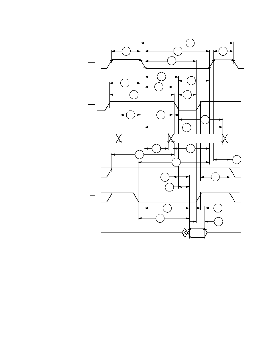
2-23
AC Electrical Characteristics
Figure 2-16. DRAM Out-of-Page Read Access
RAS
CAS
A[0≠17]
WR
RD
D[0≠23]
Data
Row Address
Column Address
In
157
163
165
162
162
169
170
171
168
167
164
166
173
174
175
172
177
176
191
160
178
159
193
161
192
158
179
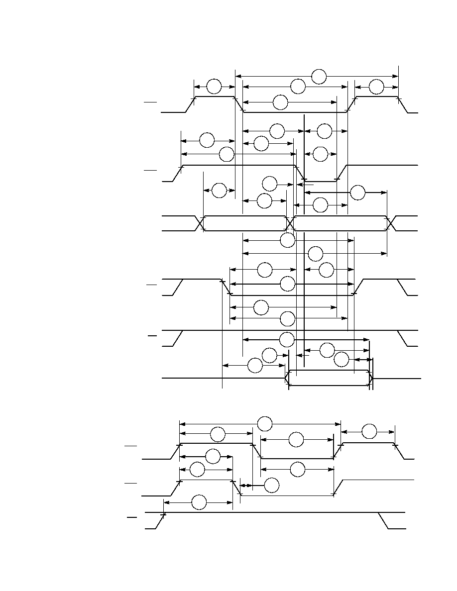
2-24
AC Electrical Characteristics
Figure 2-17. DRAM Out-of-Page Write Access
Figure 2-18. DRAM Refresh Access
RAS
CAS
A[0≠17]
WR
RD
D[0≠23]
Data Out
Column Address
Row Address
162
163
165
162
157
169
170
167
168
164
166
171
173
174
176
172
181
175
180
188
182
184
183
187
185
194
186
195
RAS
CAS
WR
157
163
162
162
190
170
165
189
177
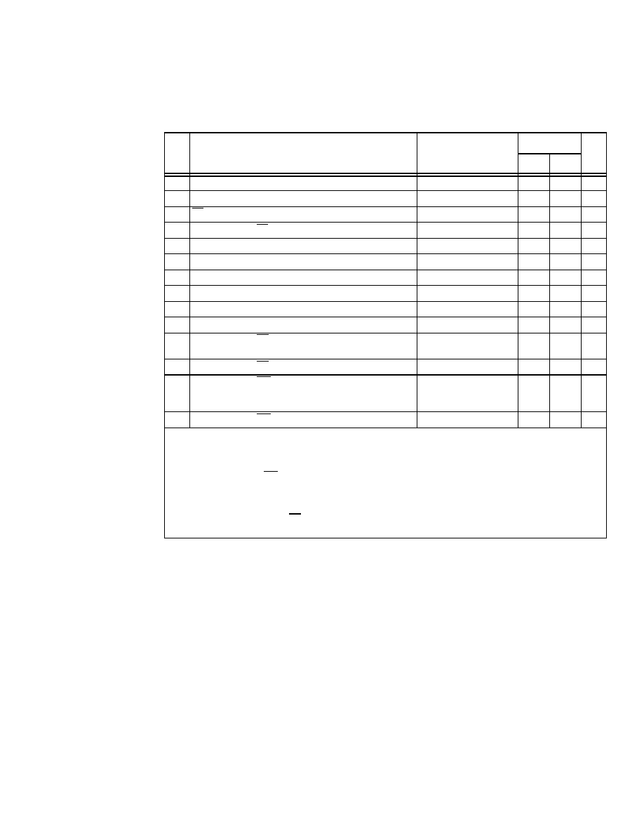
2-25
AC Electrical Characteristics
2.5.5.3 Synchronous Timings
Table 2-14. External Bus Synchronous Timings
1,2
No.
Characteristics
Expression
3,4,5
100 MHz
Unit
Min
Max
198
CLKOUT high to address, and AA valid
6
0.25
◊
T
C
+ 4.0
--
6.5
ns
199
CLKOUT high to address, and AA invalid
6
0.25
◊
T
C
2.5
--
ns
200
TA valid to CLKOUT high (set-up time)
4.0
--
ns
201
CLKOUT high to TA invalid (hold time)
0.0
--
ns
202
CLKOUT high to data out active
0.25
◊
T
C
2.5
--
ns
203
CLKOUT high to data out valid
0.25
◊
T
C
+ 4.0
--
6.5
ns
204
CLKOUT high to data out invalid
0.25
◊
T
C
2.5
--
ns
205
CLKOUT high to data out high impedance
0.25
◊
T
C
--
2.5
ns
206
Data in valid to CLKOUT high (set-up)
4.0
--
ns
207
CLKOUT high to data in invalid (hold)
0.0
--
ns
208
CLKOUT high to RD assertion
maximum: 0.75
◊
T
C
+
2.5
6.7
10.0
ns
209
CLKOUT high to RD deassertion
0.0
4.0
ns
210
CLKOUT high to WR assertion
2
maximum:
0.5
◊
T
C
+ 4.3
for WS = 1 or WS
4
for 2
WS
3
5.0
0.0
9.3
4.3
ns
ns
211
CLKOUT high to WR deassertion
0.0
3.8
ns
Notes:
1.
External bus synchronous timings should be used only for reference to the clock and not for relative
timings.
2.
Synchronous Bus Arbitration is not recommended. Use Asynchronous mode whenever possible.
3.
WS is the number of wait states specified in the BCR.
4.
If WS > 1, WR assertion refers to the next rising edge of CLKOUT.
5.
An expression is used to compute the maximum or minimum value listed, as appropriate. For timing
210, the minimum is an absolute value.
6.
T198 and T199 are valid for Address Trace mode if the ATE bit in the Operating Mode Register is set.
Use the status of BR (See T212) to determine whether the access referenced by A[0≠17] is internal or
external, when this mode is enabled.

2-26
AC Electrical Characteristics
Figure 2-19. Synchronous Bus Timings 1 WS (BCR Controlled)
WR
RD
Data Out
D[0≠23]
CLKOUT
TA
Data In
D[0≠23]
A[0≠17]
AA[0≠3]
199
201
200
211
210
208
209
207
198
205
204
203
202
206
Note: Address lines A[0≠17] hold their state after a
read or write operation. AA[0≠3] do not hold their
state after a read or write operation.
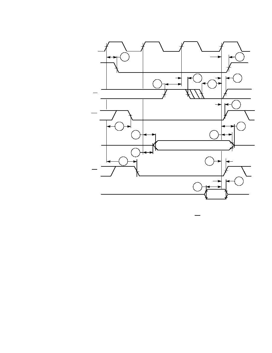
2-27
AC Electrical Characteristics
Figure 2-20. Synchronous Bus Timings 2 WS (TA Controlled)
A[0≠17]
WR
RD
Data Out
D[0≠23]
AA[0≠3]
CLKOUT
TA
Data In
D[0≠23]
198
199
201
200
201
211
209
207
208
210
200
203
202
205
204
206
Note: Address lines A[0≠17] hold their state after a
read or write operation. AA[0≠3] do not hold their
state after a read or write operation.
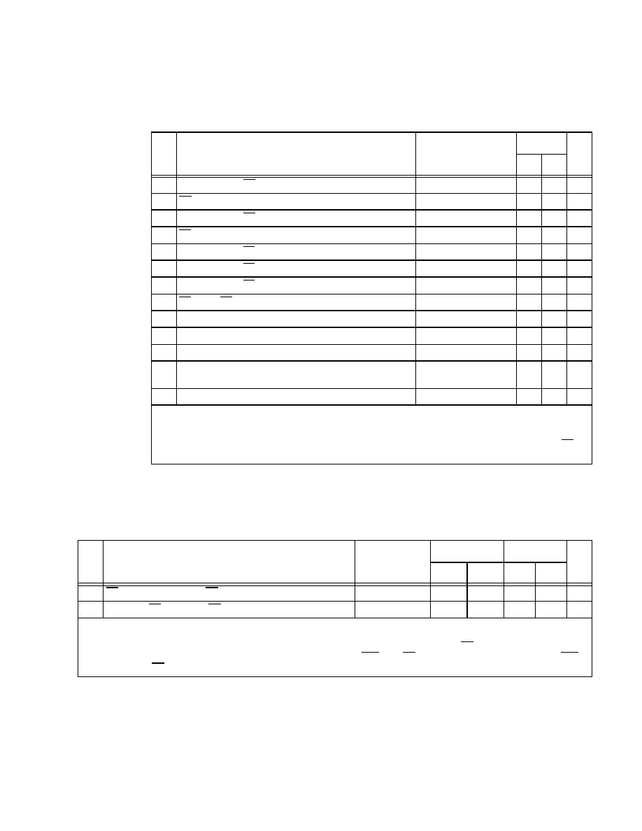
2-28
AC Electrical Characteristics
2.5.5.4 Arbitration Timings Using CLKOUT (
100 MHz only)
2.5.5.5 Asynchronous Bus Arbitration Timings
Table 2-15. Arbitration Bus Timings
1
No.
Characteristics
Expression
2
100 MHz
Unit
Min Max
212
CLKOUT high to BR assertion/deassertion
3
0.0
4.0
ns
213
BG asserted/deasserted to CLKOUT high (set-up)
4.0
--
ns
214
CLKOUT high to BG deasserted/asserted (hold)
0.0
--
ns
215
BB deassertion to CLKOUT high (input set-up)
4.0
--
ns
216
CLKOUT high to BB assertion (input hold)
0.0
--
ns
217
CLKOUT high to BB assertion (output)
0.0
4.0
ns
218
CLKOUT high to BB deassertion (output)
0.0
4.0
ns
219
BB high to BB high impedance (output)
--
4.5
ns
220
CLKOUT high to address and controls active
0.25
◊
T
C
2.5
--
ns
221
CLKOUT high to address and controls high impedance
0.75
◊
T
C
--
7.5
ns
222
CLKOUT high to AA active
0.25
◊
T
C
2.5
--
ns
223
CLKOUT high to AA deassertion
maximum: 0.25
◊
T
C
+
4.0
2.0
6.5
ns
224
CLKOUT high to AA high impedance
0.75
◊
T
C
--
7.5
ns
Notes:
1.
Synchronous Bus Arbitration is not recommended. Use Asynchronous mode whenever possible.
2.
An expression is used to compute the maximum or minimum value listed, as appropriate. For timing
223, the minimum is an absolute value.
3.
T212 is valid for Address Trace mode when the ATE bit in the Operating Mode Register is set. BR is
deasserted for internal accesses and asserted for external accesses.
Table 2-16. Asynchronous Bus Timings
No.
Characteristics
Expression
100 MHz
160 MHz
Unit
Min
Max
Min
Max
250
BB assertion window from BG input deassertion.
2.5
◊
Tc + 5
--
30
--
20.6
ns
251
Delay from BB assertion to BG assertion
2
◊
Tc + 5
25
--
17.5
--
ns
Notes:
1.
Bit 13 in the Operating Mode Register must be set to enable Asynchronous Arbitration mode.
2.
At 160 MHz, Asynchronous Arbitration mode is recommended.
3.
To guarantee timings 250 and 251, it is recommended that you assert non-overlapping BG inputs to different DSP56300
devices (on the same bus), as shown in Figure 2-21, where BG1 is the BG signal for one DSP56300 device while BG2 is
the BG signal for a second DSP56300 device.

2-29
AC Electrical Characteristics
The asynchronous bus arbitration is enabled by internal synchronization circuits on
BG
and
BB
inputs.
These synchronization circuits add delay from the external signal until it is exposed to internal logic. As a
result of this delay, a DSP56300 part may assume mastership and assert
BB
, for some time after
BG
is
deasserted. This is the reason for timing 250.
Once
BB
is asserted, there is a synchronization delay from
BB
assertion to the time this assertion is
exposed to other DSP56300 components that are potential masters on the same bus. If
BG
input is
asserted before that time, and
BG
is asserted and
BB
is deasserted, another DSP56300 component may
assume mastership at the same time. Therefore, some non-overlap period between one
BG
input active to
another
BG
input active is required. Timing 251 ensures that overlaps are avoided.
Figure 2-21. Asynchronous Bus Arbitration Timing
BG1
BB
251
BG2
250
250+251

2-30
AC Electrical Characteristics
2.5.6 Host Interface Timing
Table 2-17. Host Interface Timings
1,2,12
No.
Characteristic
10
Expression
100 MHz
160 MHz
Unit
Min
Max
Min
Max
317
Read data strobe assertion width
5
HACK assertion width
100 MHz: T
C
+ 9.9
160 MHz: T
C
+ 6.2
19.9
--
12.4
--
ns
318
Read data strobe deassertion width
5
HACK deassertion width
9.9
--
6.2
--
ns
319
Read data strobe deassertion width
5
after "Last Data Register"
reads
8,11
, or between two consecutive CVR, ICR, or ISR
reads
3
HACK deassertion width after "Last Data Register" reads
8,11
100 MHz: 2.5
◊
T
C
+ 6.6
31.6
--
20.2
--
ns
320
Write data strobe assertion width
6
13.2
--
8.3
--
ns
321
Write data strobe deassertion width
8
HACK write deassertion width
∑
after ICR, CVR and "Last Data Register" writes
∑
after IVR writes, or
after TXH:TXM:TXL writes (with HLEND= 0), or
after TXL:TXM:TXH writes (with HLEND = 1)
100 MHz: 2.5
◊
T
C
+ 6.6
160 MHz: 2.5
◊
T
C
+ 4.1
31.6
16.5
--
--
19.8
10.6
--
--
ns
ns
322
HAS assertion width
9.9
--
6.2
--
ns
323
HAS deassertion to data strobe assertion
4
0.0
--
0.0
--
ns
324
Host data input setup time before write data strobe
deassertion
6
9.9
--
6.2
--
ns
325
Host data input hold time after write data strobe deassertion
6
3.3
--
2.1
--
ns
326
Read data strobe assertion to output data active from high
impedance
5
HACK assertion to output data active from high impedance
3.3
--
2.1
--
ns
327
Read data strobe assertion to output data valid
5
HACK assertion to output data valid
--
24.5
--
16.1
ns
328
Read data strobe deassertion to output data high impedance
5
HACK deassertion to output data high impedance
--
9.9
--
6.2
ns
329
Output data hold time after read data strobe deassertion
5
Output data hold time after HACK deassertion
4.1
--
2.1
--
ns
330
HCS assertion to read data strobe deassertion
5
100 MHz: T
C
+ 9.9
160 MHz: T
C
+ 6.2
19.9
--
12.4
--
ns
331
HCS assertion to write data strobe deassertion
6
9.9
--
6.2
--
ns
332
HCS assertion to output data valid
--
19.3
--
14.0
ns
333
HCS hold time after data strobe deassertion
4
0.0
--
0.0
--
ns
334
Address (HAD[0≠7]) setup time before HAS deassertion
(HMUX=1)
4.7
--
2.9
--
ns
335
Address (HAD[0≠7]) hold time after HAS deassertion
(HMUX=1)
3.3
--
2.1
--
ns
336
HA[8≠10] (HMUX=1), HA[0≠2] (HMUX=0), HR/W setup time
before data strobe assertion
4
∑
Read
∑
Write
0
6.6
--
--
0
2.9
--
--
ns
ns
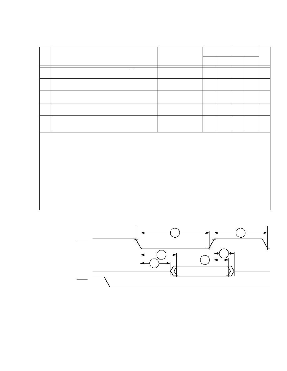
2-31
AC Electrical Characteristics
337
HA[8≠10] (HMUX=1), HA[0≠2] (HMUX=0), HR/W hold time
after data strobe deassertion
4
3.3
--
2.1
--
ns
338
Delay from read data strobe deassertion to host request
assertion for "Last Data Register" read
5, 7, 8
100 MHz: T
C
+ 5.3
160 MHz: T
C
+ 3.3
15.3
--
9.6
--
ns
ns
339
Delay from write data strobe deassertion to host request
assertion for "Last Data Register" write
6, 7, 8
100 MHz: 1.5
◊
T
C
+ 5.3
160 MHz: 1.5
◊
T
C
+ 3.3
20.3
--
12.7
--
ns
ns
340
Delay from data strobe assertion to host request deassertion
for "Last Data Register" read or write (HROD=0)
4, 7, 8
--
16.8
--
12.2
ns
341
Delay from data strobe assertion to host request deassertion
for "Last Data Register" read or write (HROD=1, open drain
host request)
4, 7, 8, 9
--
300.0
--
300.0
ns
Notes:
1.
See the Programmer's Model section in the chapter on the HI08 in the DSP56L307 User's Manual.
2.
In the timing diagrams below, the controls pins are drawn as active low. The pin polarity is programmable.
3.
This timing is applicable only if two consecutive reads from one of these registers are executed.
4.
The data strobe is Host Read (HRD) or Host Write (HWR) in the Dual Data Strobe mode and Host Data Strobe (HDS) in
the Single Data Strobe mode.
5.
The read data strobe is HRD in the Dual Data Strobe mode and HDS in the Single Data Strobe mode.
6.
The write data strobe is HWR in the Dual Data Strobe mode and HDS in the Single Data Strobe mode.
7.
The host request is HREQ in the Single Host Request mode and HRRQ and HTRQ in the Double Host Request mode.
8.
The "Last Data Register" is the register at address $7, which is the last location to be read or written in data transfers. This
is RXL/TXL in the Big Endian mode (HLEND = 0; HLEND is the Interface Control Register bit 7--ICR[7]), or RXH/TXH in
the Little Endian mode (HLEND = 1).
9.
In this calculation, the host request signal is pulled up by a 4.7 k
resistor in the Open-drain mode.
10. V
CCQH
= 3.3 V
±
0.3 V, V
CC
= 1.8 V
±
0.1 V; T
J
=
≠40∞C to +100 ∞C, C
L
= 50 pF
11.
This timing is applicable only if a read from the "Last Data Register" is followed by a read from the RXL, RXM, or RXH
registers without first polling RXDF or HREQ bits, or waiting for the assertion of the HREQ signal.
12. After the external host writes a new value to the ICR, the HI08 is ready for operation after three DSP clock cycles (3
◊
Tc).
Figure 2-22. Host Interrupt Vector Register (IVR) Read Timing Diagram
Table 2-17. Host Interface Timings
1,2,12
(Continued)
No.
Characteristic
10
Expression
100 MHz
160 MHz
Unit
Min
Max
Min
Max
HACK
H[0≠7]
HREQ
329
317
318
328
326
327
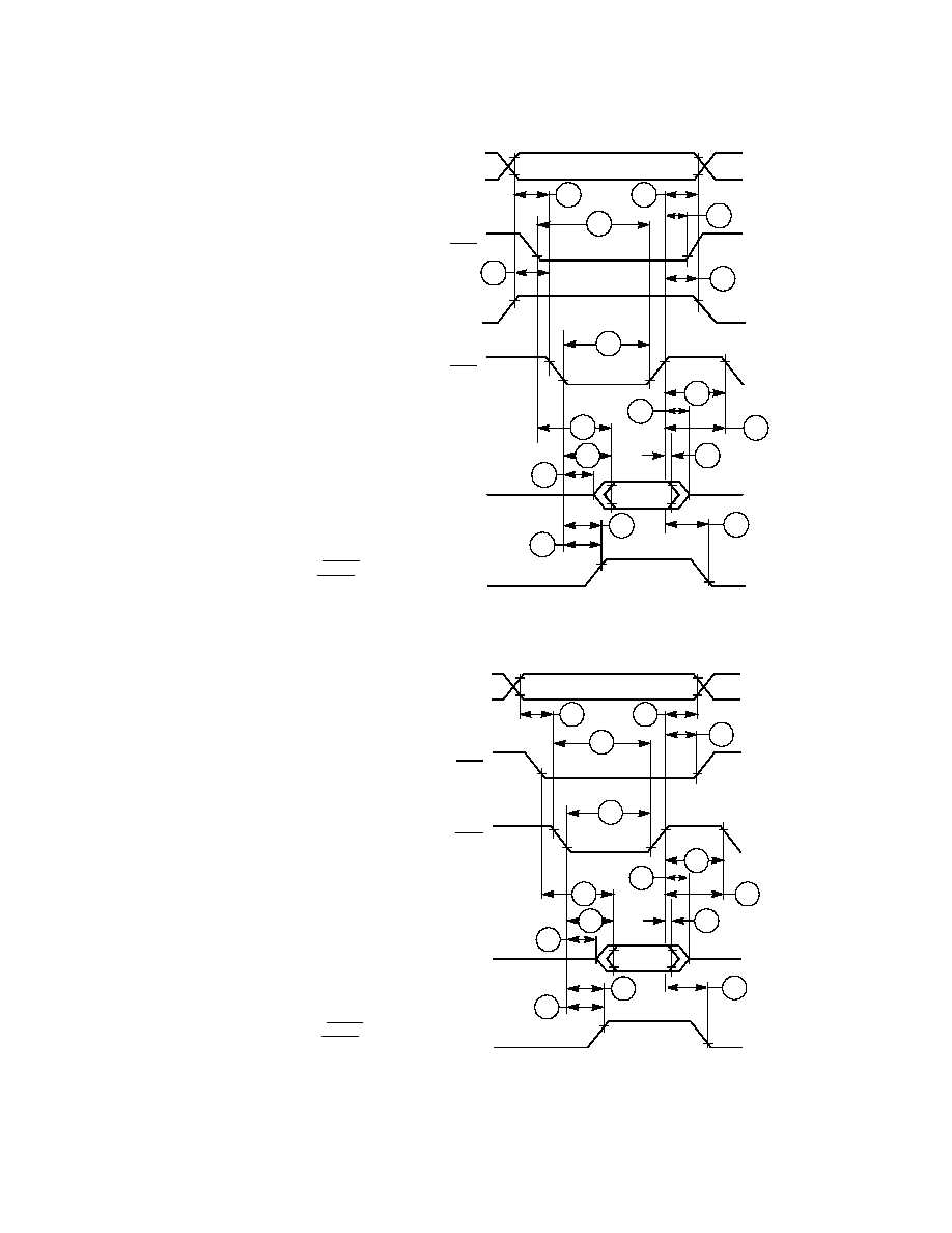
2-32
AC Electrical Characteristics
Figure 2-23. Read Timing Diagram, Non-Multiplexed Bus, Single Data Strobe
Figure 2-24. Read Timing Diagram, Non-Multiplexed Bus, Double Data Strobe
HDS
HA[2≠0]
HCS
H[7≠0]
327
332
319
318
317
330
329
337
336
328
326
338
341
340
333
HREQ (single host request)
HRW
336
337
HRRQ (double host request)
HRD
HA[2≠0]
HCS
H[7≠0]
327
332
319
318
317
330
329
337
336
328
326
338
341
340
333
HREQ (single host request)
HRRQ (double host request)

2-33
AC Electrical Characteristics
Figure 2-25. Write Timing Diagram, Non-Multiplexed Bus, Single Data Strobe
Figure 2-26. Write Timing Diagram, Non-Multiplexed Bus, Double Data Strobe
HDS
HA[2≠0]
HCS
H[7≠0]
324
321
320
331
337
336
339
341
340
333
HREQ (single host request)
HRW
336
337
HTRQ (double host request)
325
HWR
HA[2≠0]
HCS
H[7≠0]
324
321
320
331
325
337
336
339
341
340
333
HREQ (single host request)
HTRQ (double host request)
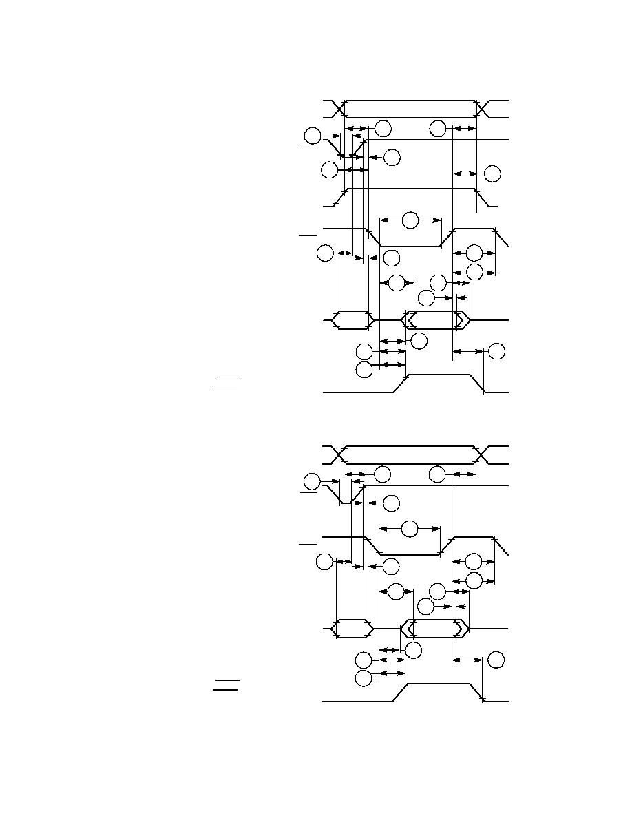
2-34
AC Electrical Characteristics
,
Figure 2-27. Read Timing Diagram, Multiplexed Bus, Single Data Strobe
Figure 2-28. Read Timing Diagram, Multiplexed Bus, Double Data Strobe
HDS
HA[10≠8]
HAS
HAD[7≠0]
HREQ (single host request)
Address
Data
317
318
319
328
329
327
326
335
336
337
334
341
340
338
323
322
HRRQ (double host request)
HRW
336
337
HRD
HA[10≠8]
HAS
HAD[7≠0]
Address
Data
317
318
319
328
329
327
326
335
336
337
334
341
340
338
323
322
HREQ (single host request)
HRRQ (double host request)

2-35
AC Electrical Characteristics
,
Figure 2-29. Write Timing Diagram, Multiplexed Bus, Single Data Strobe
Figure 2-30. Write Timing Diagram, Multiplexed Bus, Double Data Strobe
HDS
HA[10≠8]
HREQ (single host request)
HAS
HAD[7≠0]
Address
Data
320
321
325
324
335
341
339
336
334
340
322
323
HRW
336
337
HTRQ (double host request)
337
HWR
HA[10≠8]
HAS
HAD[7≠0]
Address
Data
320
321
325
324
335
341
339
336
334
340
322
323
HREQ (single host request)
HTRQ (double host request)
337
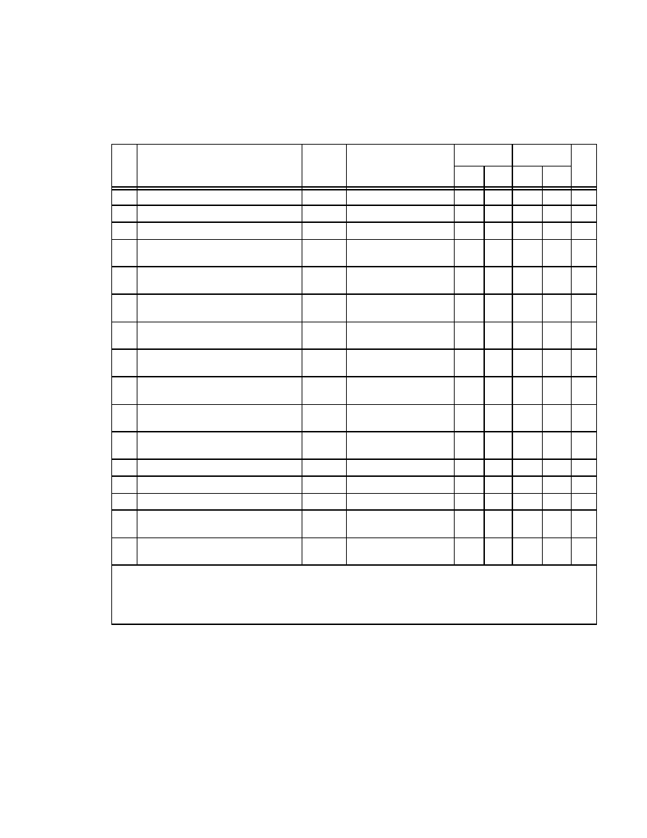
2-36
AC Electrical Characteristics
2.5.7 SCI Timing
Table 2-18. SCI Timings
No.
Characteristics
1
Symbol
Expression
100 MHz
160 MHz
Unit
Min
Max
Min
Max
400
Synchronous clock cycle
t
SCC
2
8
◊
T
C
80
--
50
--
ns
401
Clock low period
t
SCC
/2
-
10.0
30.0
--
15.0
--
ns
402
Clock high period
t
SCC
/2
-
10.0
30.0
--
15.0
--
ns
403
Output data setup to clock falling edge
(internal clock)
t
SCC
/4 + 0.5
◊
T
C
-
10.0
8.0
--
0.0
--
ns
404
Output data hold after clock rising edge
(internal clock)
t
SCC
/4
-
0.5
◊
T
C
15.0
--
9.4
--
ns
405
Input data setup time before clock rising
edge (internal clock)
t
SCC
/4 + 0.5
◊
T
C
+ 25.0
50.0
--
40.6
--
ns
406
Input data not valid before clock rising
edge (internal clock)
t
SCC
/4 + 0.5
◊
T
C
-
5.5
--
19.5
--
10.1
ns
407
Clock falling edge to output data valid
(external clock)
--
32.0
--
32.0
ns
408
Output data hold after clock rising edge
(external clock)
T
C
+ 8.0
18.0
--
14.3
--
ns
409
Input data setup time before clock rising
edge (external clock)
0.0
--
0.0
--
ns
410
Input data hold time after clock rising edge
(external clock)
9.0
--
9.0
--
ns
411
Asynchronous clock cycle
t
ACC
3
64
◊
T
C
640.0
--
400.0
--
ns
412
Clock low period
t
ACC
/2
-
10.0
310.0
--
190.0
--
ns
413
Clock high period
t
ACC
/2
-
10.0
310.0
--
190.0
--
ns
414
Output data setup to clock rising edge
(internal clock)
t
ACC
/2
-
30.0
290.0
--
170.0
--
ns
415
Output data hold after clock rising edge
(internal clock)
t
ACC
/2
-
30.0
290.0
--
170.0
--
ns
Notes:
1.
V
CCQH
= 3.3 V
±
0.3 V, V
CC
= 1.8 V
±
0.1 V; T
J
=
≠40∞C to +100 ∞C, C
L
= 50 pF.
2.
t
SCC
= synchronous clock cycle time (for internal clock, t
SCC
is determined by the SCI clock control register and
T
C
).
3.
t
ACC
= asynchronous clock cycle time; value given for 1X Clock mode (for internal clock, t
ACC
is determined by
the SCI clock control register and T
C
).
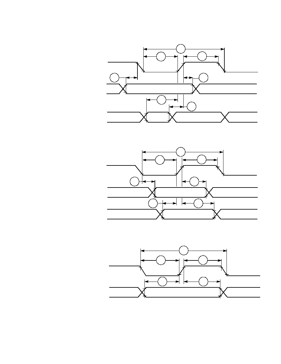
2-37
AC Electrical Characteristics
Figure 2-31. SCI Synchronous Mode Timing
Figure 2-32. SCI Asynchronous Mode Timing
a) Internal Clock
Data Valid
Data
Valid
b) External Clock
Data Valid
SCLK
(Output)
TXD
RXD
SCLK
(Input)
TXD
RXD
Data Valid
400
402
404
401
403
405
406
400
402
401
407
409
410
408
1X SCLK
(Output)
TXD
Data Valid
413
411
412
414
415
2-38
AC Electrical Characteristics
ESSI0/ESSI1 Timing
Table 2-19. ESSI Timings at 100 MHz
No.
Characteristics
1, 2, 3
Symbol
Expression
Min Max
Condi-
tion
4
Unit
430
Clock cycle
5
t
SSICC
3
◊
T
C
4
◊
T
C
30.0
40.0
--
--
x ck
i ck
ns
431
Clock high period
For internal clock
For external clock
--
2
◊
T
C
-
10.0
1.5
◊
T
C
10.0
15.0
--
--
ns
ns
432
Clock low period
For internal clock
For external clock
--
2
◊
T
C
-
10.0
1.5
◊
T
C
10.0
15.0
--
--
ns
ns
433
RXC rising edge to FSR out (bl) high
--
--
--
--
37.0
22.0
x ck
i ck a
ns
434
RXC rising edge to FSR out (bl) low
--
--
--
--
37.0
22.0
x ck
i ck a
ns
435
RXC rising edge to FSR out (wr) high
6
--
--
--
--
39.0
24.0
x ck
i ck a
ns
436
RXC rising edge to FSR out (wr) low
6
--
--
--
--
39.0
24.0
x ck
i ck a
ns
437
RXC rising edge to FSR out (wl) high
--
--
--
--
36.0
21.0
x ck
i ck a
ns
438
RXC rising edge to FSR out (wl) low
--
--
--
--
37.0
22.0
x ck
i ck a
ns
439
Data in setup time before RXC (SCK in
Synchronous mode) falling edge
--
--
0.0
19.0
--
--
x ck
i ck
ns
440
Data in hold time after RXC falling edge
--
--
5.0
3.0
--
--
x ck
i ck
ns
441
FSR input (bl, wr) high before RXC falling edge
6
--
--
23.0
1.0
--
--
x ck
i ck a
ns
442
FSR input (wl) high before RXC falling edge
--
--
23.0
1.0
--
--
x ck
i ck a
ns
443
FSR input hold time after RXC falling edge
--
--
3.0
0.0
--
--
x ck
i ck a
ns
444
Flags input setup before RXC falling edge
--
--
0.0
19.0
--
--
x ck
i ck s
ns
445
Flags input hold time after RXC falling edge
--
--
6.0
0.0
--
--
x ck
i ck s
ns
446
TXC rising edge to FST out (bl) high
--
--
--
--
29.0
15.0
x ck
i ck
ns
447
TXC rising edge to FST out (bl) low
--
--
--
--
31.0
17.0
x ck
i ck
ns
448
TXC rising edge to FST out (wr) high
6
--
--
--
--
31.0
17.0
x ck
i ck
ns
449
TXC rising edge to FST out (wr) low
6
--
--
--
--
33.0
19.0
x ck
i ck
ns
2-39
AC Electrical Characteristics
450
TXC rising edge to FST out (wl) high
--
--
--
--
30.0
16.0
x ck
i ck
ns
451
TXC rising edge to FST out (wl) low
--
--
--
--
31.0
17.0
x ck
i ck
ns
452
TXC rising edge to data out enable from high
impedance
--
--
--
--
31.0
17.0
x ck
i ck
ns
453
TXC rising edge to Transmitter #0 drive enable
assertion
--
--
--
--
34.0
20.0
x ck
i ck
ns
454
TXC rising edge to data out valid
--
35 + 0.5
◊
T
C
--
--
40.0
21.0
x ck
i ck
ns
455
TXC rising edge to data out high impedance
7
--
--
--
--
31.0
16.0
x ck
i ck
ns
456
TXC rising edge to Transmitter #0 drive enable
deassertion
7
--
--
--
--
34.0
20.0
x ck
i ck
ns
457
FST input (bl, wr) setup time before TXC falling
edge
6
--
--
2.0
21.0
--
--
x ck
i ck
ns
458
FST input (wl) to data out enable from high
impedance
--
--
--
27.0
--
ns
459
FST input (wl) to Transmitter #0 drive enable
assertion
--
--
--
31.0
--
ns
460
FST input (wl) setup time before TXC falling edge
--
--
2.0
21.0
--
--
x ck
i ck
ns
461
FST input hold time after TXC falling edge
--
--
4.0
0.0
--
--
x ck
i ck
ns
462
Flag output valid after TXC rising edge
--
--
--
--
32.0
18.0
x ck
i ck
ns
Notes:
1.
V
CCQL
= 2.5 V
±
0.25 V; T
J
=
-
40∞C to +100 ∞C, C
L
= 50 pF
2.
i ck = Internal Clock
x ck = External Clock
i ck a = Internal Clock, Asynchronous Mode
(Asynchronous implies that TXC and RXC are two different clocks)
i ck s = Internal Clock, Synchronous Mode
(Synchronous implies that TXC and RXC are the same clock)
3.
bl = bit length
wl = word length
wr = word length relative
4.
TXC (SCK Pin) = Transmit Clock
RXC (SC0 or SCK Pin) = Receive Clock
FST (SC2 Pin) = Transmit Frame Sync
FSR (SC1 or SC2 Pin) Receive Frame Sync
5.
For the internal clock, the external clock cycle is defined by Icyc and the ESSI control register.
6.
The word-relative frame sync signal waveform relative to the clock operates the same way as the
bit-length frame sync signal waveform, but it spreads from one serial clock before first bit clock (same
as Bit Length Frame Sync signal), until the one before last bit clock of the first word in frame.
7.
Periodically sampled and not 100 per cent tested
Table 2-19. ESSI Timings at 100 MHz (Continued)
No.
Characteristics
1, 2, 3
Symbol
Expression
Min Max
Condi-
tion
4
Unit

2-40
AC Electrical Characteristics
Table 2-8. ESSI Timings at 160 MHz
No.
Characteristics
1,2,3
Symbol
Expression
Min Max
Condi-
tion
4
Unit
430
Clock cycle
5
t
SSICC
8
◊
T
C
6
◊
T
C
50.0
37.5
--
--
i ck
x ck
ns
431
Clock high period
For internal clock
For external clock
4
◊
T
C
-
10.0
3
◊
T
C
15.0
18.8
--
--
ns
ns
432
Clock low period
For internal clock
For external clock
4
◊
T
C
-
10.0
3
◊
T
C
15.0
18.8
--
--
ns
ns
433
RXC rising edge to FSR out (bl) high
--
--
37.0
22.0
x ck
i ck a
ns
434
RXC rising edge to FSR out (bl) low
--
--
37.0
22.0
x ck
i ck a
ns
435
RXC rising edge to FSR out (wr) high
6
--
--
39.0
24.0
x ck
i ck a
ns
436
RXC rising edge to FSR out (wr) low
6
--
--
39.0
24.0
x ck
i ck a
ns
437
RXC rising edge to FSR out (wl) high
--
--
36.0
21.0
x ck
i ck a
ns
438
RXC rising edge to FSR out (wl) low
--
--
37.0
22.0
x ck
i ck a
ns
439
Data in setup time before RXC (SCK in
Synchronous mode) falling edge
0.0
19.0
--
--
x ck
i ck
ns
440
Data in hold time after RXC falling edge
5.0
3.0
--
--
x ck
i ck
ns
441
FSR input (bl, wr) high before RXC falling edge
6
1.0
6.0
--
--
x ck
i ck a
ns
442
FSR input (wl) high before RXC falling edge
1.0
6.0
--
--
x ck
i ck a
ns
443
FSR input hold time after RXC falling edge
3.0
0.0
--
--
x ck
i ck a
ns
444
Flags input setup before RXC falling edge
0.0
19.0
--
--
x ck
i ck s
ns
445
Flags input hold time after RXC falling edge
6.0
0.0
--
--
x ck
i ck s
ns
446
TXC rising edge to FST out (bl) high
--
--
29.0
15.0
x ck
i ck
ns
447
TXC rising edge to FST out (bl) low
--
--
31.0
17.0
x ck
i ck
ns
448
TXC rising edge to FST out (wr) high
6
--
--
31.0
17.0
x ck
i ck
ns
449
TXC rising edge to FST out (wr) low
6
--
--
33.0
19.0
x ck
i ck
ns
450
TXC rising edge to FST out (wl) high
--
--
30.0
16.0
x ck
i ck
ns
451
TXC rising edge to FST out (wl) low
--
--
31.0
17.0
x ck
i ck
ns
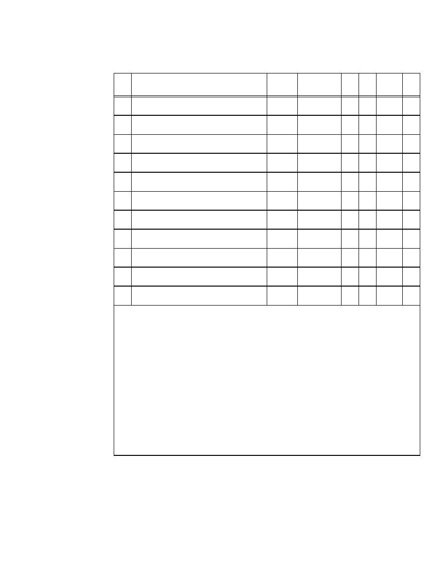
2-41
AC Electrical Characteristics
452
TXC rising edge to data out enable from high
impedance
--
--
31.0
17.0
x ck
i ck
ns
453
TXC rising edge to Transmitter #0 drive enable
assertion
--
--
34.0
20.0
x ck
i ck
ns
454
TXC rising edge to data out valid
35 + 0.5
◊
T
C
--
--
38.1
21.0
x ck
i ck
ns
455
TXC rising edge to data out high impedance
7
--
--
31.0
16.0
x ck
i ck
ns
456
TXC rising edge to Transmitter #0 drive enable
deassertion
7
--
--
34.0
20.0
x ck
i ck
ns
457
FST input (bl, wr) setup time before TXC falling
edge
6
2.0
21.0
--
--
x ck
i ck
ns
458
FST input (wl) to data out enable from high
impedance
--
27.0
--
ns
459
FST input (wl) to Transmitter #0 drive enable
assertion
--
31.0
--
ns
460
FST input (wl) setup time before TXC falling edge
2.0
21.0
--
--
x ck
i ck
ns
461
FST input hold time after TXC falling edge
4.0
0.0
--
--
x ck
i ck
ns
462
Flag output valid after TXC rising edge
--
--
32.0
18.0
x ck
i ck
ns
Notes:
1.
V
CCQL
= 2.5 V
±
0.25 V; T
J
=
-
40∞C to +100 ∞C, C
L
= 50 pF
2.
i ck = Internal Clock
x ck = External Clock
i ck a = Internal Clock, Asynchronous Mode
(Asynchronous implies that TXC and RXC are two different clocks)
i ck s = Internal Clock, Synchronous Mode
(Synchronous implies that TXC and RXC are the same clock)
3.
bl = bit length
wl = word length
wr = word length relative
4.
TXC (SCK Pin) = Transmit Clock
RXC (SC0 or SCK Pin) = Receive Clock
FST (SC2 Pin) = Transmit Frame Sync
FSR (SC1 or SC2 Pin) Receive Frame Sync
5.
For the internal clock, the external clock cycle is defined by I
CYC
and the ESSI Control Register
(SSICR).
6.
The word-relative frame sync signal waveform relative to the clock operates in the same manner as the
bit-length frame sync signal waveform, but it spreads from one serial clock before first bit clock (same
as Bit Length Frame Sync signal), until the one before last bit clock of the first word in frame.
7.
Periodically sampled and not 100 per cent tested
Table 2-8. ESSI Timings at 160 MHz (Continued)
No.
Characteristics
1,2,3
Symbol
Expression
Min Max
Condi-
tion
4
Unit

2-42
AC Electrical Characteristics
Figure 2-1. ESSI Transmitter Timing
Last Bit
See Note
Note:
In Network mode, output flag transitions can occur at the start of each time slot within the frame. In
Normal mode, the output flag state is asserted for the entire frame period.
First Bit
430
432
446
447
450
451
455
454
454
452
459
456
453
461
457
458
460
461
462
431
TXC
(Input/
Output)
FST (Bit)
Out
FST (Word)
Out
Data Out
Transmitter
#0 Drive
Enable
FST (Bit) In
FST (Word)
In
Flags Out
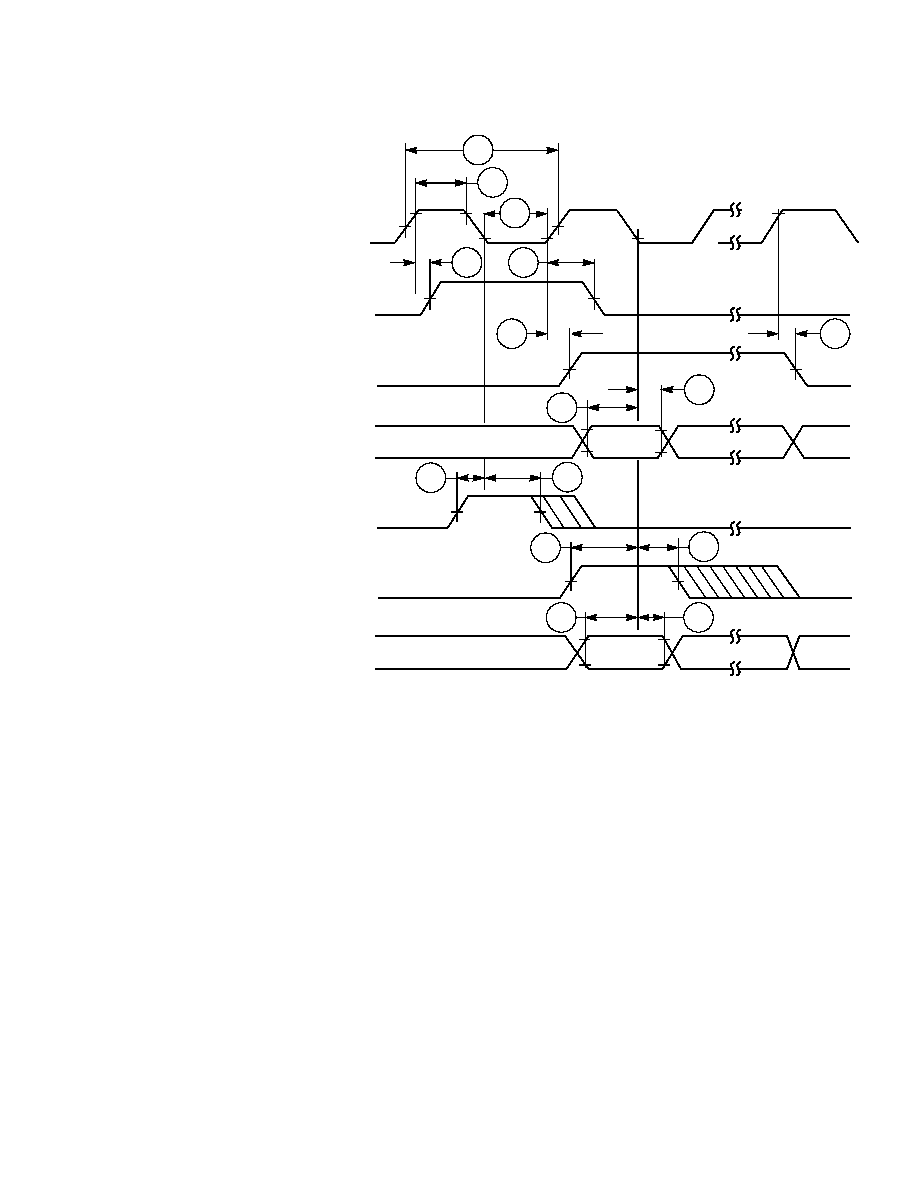
2-43
AC Electrical Characteristics
Figure 2-2. ESSI Receiver Timing
Last Bit
First Bit
430
432
433
437
438
440
439
443
441
442
443
445
444
431
434
RXC
(Input/
Output)
FSR (Bit)
Out
FSR
(Word)
Out
Data In
FSR (Bit)
In
FSR
(Word)
In
Flags In
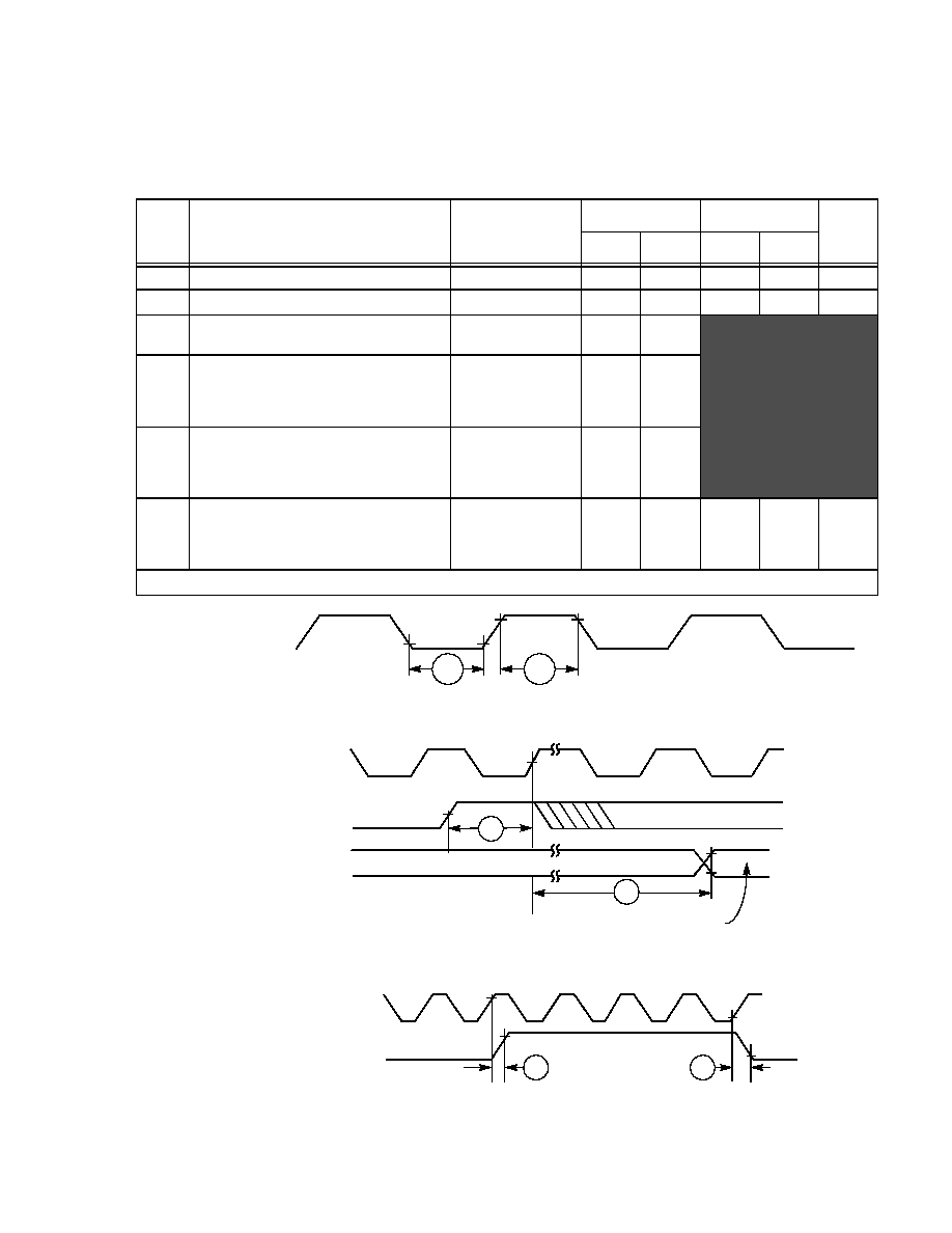
2-44
AC Electrical Characteristics
2.5.9 Timer Timing
Table 2-1. Timer Timings
No.
Characteristics
Expression
100 MHz
160 MHz
Unit
Min
Max
Min
Max
480
TIO Low
2
◊
T
C
+ 2.0
22.0
--
14.5
--
ns
481
TIO High
2
◊
T
C
+ 2.0
22.0
--
14.5
--
ns
482
Timer set-up time from TIO (Input) assertion
to CLKOUT rising edge
9.0
10.0
483
Synchronous timer delay time from CLKOUT
rising edge to the external memory access
address out valid caused by first interrupt
instruction execution
10.25
◊
T
C
+ 1.0
103.5
--
484
CLKOUT rising edge to TIO (Output)
assertion
∑
Minimum
∑
Maximum
0.5
◊
T
C
+ 0.5
0.5
◊
T
C
+ 19.8
5.5
--
--
24.8
486
Synchronous delay time from Timer input
rising edge to the external memory address
out valid caused by the first interrupt
instruction execution
10.25
◊
T
C
+ 10.0
112.5
--
74.06
--
ns
Note:
V
CCQH
= 3.3 V
±
0.3 V, V
CC
= 1.8 V
±
0.1 V; T
J
=
≠40∞C to +100 ∞C, C
L
= 50 pF
Figure 2-3. TIO Timer Event Input Restrictions
Figure 2-4. Timer Interrupt Generation
Figure 2-5. External Pulse Generation
TIO
481
480
CLKOUT
TIO (Input)
First Interrupt Instruction Execution
Address
482
483
CLKOUT
TIO (Output)
484
485
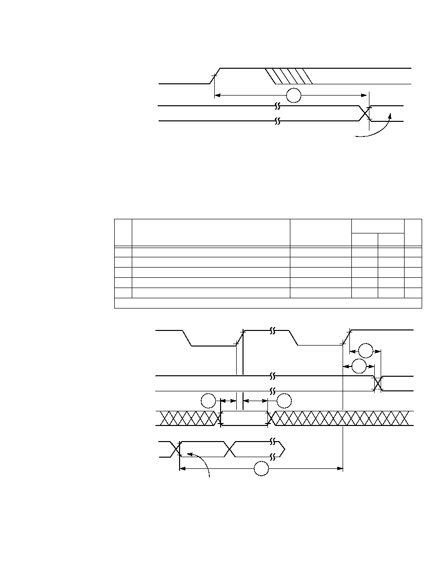
2-45
AC Electrical Characteristics
2.5.10 CONSIDERATIONS FOR GPIO USE
2.5.10.1 Operating Frequency of 100 MHz or Less
Figure 2-6. Timer Interrupt Generation
Table 2-2. GPIO Timing
No.
Characteristics
Expression
100 MHz
Unit
Min
Max
490
CLKOUT edge to GPIO out valid (GPIO out delay time)
--
8.5
ns
491
CLKOUT edge to GPIO out not valid (GPIO out hold time)
0.0
--
ns
492
GPIO In valid to CLKOUT edge (GPIO in set-up time)
8.5
--
ns
493
CLKOUT edge to GPIO in not valid (GPIO in hold time)
0.0
--
ns
494
Fetch to CLKOUT edge before GPIO change
Minimum: 6.75
◊
T
C
67.5
--
ns
Note:
V
CC
= 3.3 V
±
0.3 V; T
J
=
-
40∞C to +100 ∞C, C
L
= 50 pF
Figure 2-7. GPIO Timing
TIO (Input)
First Interrupt Instruction Execution
Address
486
Valid
GPIO
(Input)
GPIO
(Output)
CLKOUT
(Output)
Fetch the instruction MOVE X0,X:(R0); X0 contains the new value of GPIO
and R0 contains the address of the GPIO data register.
A[0≠17]
490
491
492
494
493

2-46
AC Electrical Characteristics
2.5.10.2 With an Operating Frequency above 100 MHz
The following considerations can be helpful when GPIO is used for output or input with an operating
frequency above 100 MHz (that is, when
CLKOUT
is not available).
∑ GPIO as Output:
-- The time from fetch of the instruction that changes the GPIO pin to the actual change is seven core
clock cycles. This is true, assuming that the instruction is a on
e
-cycle instruction and that there are
no pipeline stalls or any other pipeline delays.
-- The maximum rise or fall time of a GPIO pin is 13 ns (TTL levels, assuming that the maximum of
50 pF load limit is met).
∑ GPIO as Input--GPIO inputs are not synchronized with the core clock. When only one GPIO bit is
polled, this lack of synchronization presents no problem, since the read value can be either the previous
value or the new value of the corresponding GPIO pin. However, there is the risk of reading an
intermediate state if:
-- Two or more GPIO bits are treated as a coupled group (for example, four possible status states
encoded in two bits).
-- The read operation occurs during a simultaneous change of GPIO pins (for example, the change of
00 to 11 may happen through an intermediate state of 01 or 10).
Therefore, when GPIO bits are read, the recommended practice is to poll continuously until two
consecutive read operations have identical results.

2-47
AC Electrical Characteristics
2.5.11 JTAG Timing
Table 2-3. JTAG Timing
No.
Characteristics
All frequencies
Unit
Min Max
500
TCK frequency of operation (1/(T
C
◊
3); maximum 22 MHz)
0.0
22.0
MHz
501
TCK cycle time in Crystal mode
45.0
--
ns
502
TCK clock pulse width measured at 1.5 V
20.0
--
ns
503
TCK rise and fall times
0.0
3.0
ns
504
Boundary scan input data setup time
5.0
--
ns
505
Boundary scan input data hold time
24.0
--
ns
506
TCK low to output data valid
0.0
40.0
ns
507
TCK low to output high impedance
0.0
40.0
ns
508
TMS, TDI data setup time
5.0
--
ns
509
TMS, TDI data hold time
25.0
--
ns
510
TCK low to TDO data valid
0.0
44.0
ns
511
TCK low to TDO high impedance
0.0
44.0
ns
512
TRST assert time
100.0
--
ns
513
TRST setup time to TCK low
40.0
--
ns
Notes:
1.
V
CCQH
= 3.3 V
±
0.3 V, V
CC
= 1.8 V
±
0.1 V; T
J
=
≠40∞C to +100 ∞C, C
L
= 50 pF
2.
All timings apply to OnCE module data transfers because it uses the JTAG port as an interface.
Figure 2-8. Test Clock Input Timing Diagram
TCK
(Input)
V
M
V
M
V
IH
V
IL
501
502
502
503
503

2-48
AC Electrical Characteristics
Figure 2-9. Boundary Scan (JTAG) Timing Diagram
Figure 2-10. Test Access Port Timing Diagram
Figure 2-11. TRST Timing Diagram
TCK
(Input)
Data
Inputs
Data
Outputs
Data
Outputs
Data
Outputs
V
IH
V
IL
Input Data Valid
Output Data Valid
Output Data Valid
505
504
506
507
506
TCK
(Input)
TDI
(Input)
TDO
(Output)
TDO
(Output)
TDO
(Output)
V
IH
V
IL
Input Data Valid
Output Data Valid
Output Data Valid
TMS
508
509
510
511
510
TCK
(Input)
TRST
(Input)
513
512
2-49
AC Electrical Characteristics
2.5.12 OnCE Module TimIng
Table 2-4. OnCE Module Timing
No.
Characteristics
Expression
Min
Max
Unit
500
TCK frequency of operation
Max 22.0 MHz
0.0
22.0
MHz
514
DE assertion time in order to enter Debug mode
1.5
◊
T
C
+ 10.0
20.0
--
ns
515
Response time when DSP56L307 is executing NOP
instructions from internal memory
5.5
◊
T
C
+ 30.0
--
67.0
ns
516
Debug acknowledge assertion time
3
◊
T
C
+
5.0
25.0
--
ns
Note:
V
CCQH
= 3.3 V
±
0.3 V, V
CC
= 1.8 V
±
0.1 V; T
J
= ≠40∞C to +100 ∞C, C
L
= 50 pF
Figure 2-12. OnCE--Debug Request
DE
516
515
514

2-50
AC Electrical Characteristics

3-1
Chapter 3
Packaging
3.1 Pin-Out and Package Information
This section includes diagrams of the DSP56L307 package pin-outs and tables showing how the
signals described in Chapter 1 are allocated for the package.
The DSP56L307 is available in a
196-pin Molded Array Process-Ball Grid Array (MAP-BGA) package.

3-2
MAP-BGA Package Description
3.2 MAP-BGA Package Description
Top and bottom views of the MAP-BGA package are shown in Figure 3-1 and Figure 3-2 with their
pin-outs.
Figure 3-1. DSP56L307 MAP-BGA Package, Top View
DSP56L307
Top View
1
3
4
2
5
6
7
8
10
14
13
12
11
9
V
CCQH
HACK
HREQ
B
C
D
E
F
G
H
N
M
L
J
K
HA0
HRW
HDS
HCS
IRQD
H5
NC
H7
HA1
HA2
H2
V
CCD
V
CCQL
IRQA
D19
D18
V
CCD
V
CCD
V
CCQL
V
CCS
V
CCQH
GND
GND
GND
GND
GND
GND
GND
GND
GND
GND
GND
GND
GND
GND
GND
GND
GND
GND
GND
GND
GND
GND
GND
GND
GND
GND
GND
GND
GND
GND
V
CCA
V
CCC
V
CCA
V
CCA
V
CCP
V
CCH
V
CCS
V
CCQL
GND
GND
GND
GND
GND
GND
V
CCD
V
CCQH
IRQC
H4
H6
V
CCQL
D12
D11
D15
D9
D5
D3
D0
A0
A17
A16
A1
A2
H1
H0
H3
TIO1
RXD
TIO2
TIO0
SCK1
TXD
SC12
SC11
STD1
SCK0
SRD0
SRD1
STD0
SC02
SC01
TDO
TMS
DE
TA
TDI
TCK
A15
A12
A7
A5
BG
GND
P
PINIT
AA0
TRST
SCLK
V
CCC
P
A
IRQB
D23
D22
D21
D20
D17
D16
D14
D13
D10
D8
D7
D6
D4
D2
D1
A14
A13
A11
A10
A9
A8
A6
A4
A3
AA1
RD
WR
BB
BR
BCLK
XTAL
CAS
AA3
AA2
GND
P1
PCAP
RESET
SC00
SC10
NC
NC
NC
NC
GND
GND
GND
GND
GND
GND
GND
GND
GND
GND
GND
GND
GND
GND
GND
GND
GND
GND
GND
GND
GND
GND
GND
GND
GND
GND
GND
GND
EXTAL
BCLK
CLKOUT

3-3
MAP-BGA Package Description
Figure 3-2. DSP56L307 MAP-BGA Package, Bottom View
1
3
4
2
5
6
7
8
10
14
13
12
11
9
V
CCQH
HACK
HREQ
B
C
D
E
F
G
H
N
M
L
J
K
HA0
HRW
HDS
HCS
IRQD
H5
NC
H7
HA1
HA2
H2
V
CCD
V
CCQL
IRQA
D19
D18
V
CCD
V
CCD
V
CCQL
V
CCS
V
CCQH
GND
GND
GND
GND
GND
GND
GND
GND
GND
GND
GND
GND
GND
GND
GND
GND
GND
GND
GND
GND
GND
GND
GND
GND
GND
GND
GND
GND
GND
GND
V
CCA
V
CCC
V
CCA
V
CCA
V
CCP
V
CCH
V
CCS
V
CCQL
GND
GND
GND
GND
GND
GND
V
CCD
V
CCQH
IRQC
H4
H6
V
CCQL
D12
D11
D15
D9
D5
D3
D0
A0
A17
A16
A1
A2
H1
H0
H3
TIO1
RXD
TIO2
TIO0
SCK1
TXD
SC12
SC11
STD1
SCK0
SRD0
SRD1
STD0
SC02
SC01
TDO
TMS
DE
TA
TDI
TCK
A15
A12
A7
A5
BG
GND
P
PINIT
AA0
TRST
SCLK
V
CCC
P
A
IRQB
D23
D22
D21
D20
D17
D16
D14
D13
D10
D8
D7
D6
D4
D2
D1
A14
A13
A11
A10
A9
A8
A6
A4
A3
AA1
RD
WR
BB
BR
XTAL
CAS
AA3
AA2
GND
P1
PCAP
RESET
SC00
SC10
NC
NC
NC
NC
GND
GND
GND
GND
GND
GND
GND
GND
GND
GND
GND
GND
GND
GND
GND
GND
GND
GND
GND
GND
GND
GND
GND
GND
GND
GND
GND
GND
EXTAL
Bottom View
CLKOUT
BCLK
BCLK
3-4
MAP-BGA Package Description
Table 3-1. Signal List by Ball Number
Ball
No.
Signal Name
Ball
No.
Signal Name
Ball
No.
Signal Name
A1
Not Connected (NC),
reserved
B12
D8
D9
GND
A2
SC11 or PD1
B13
D5
D10
GND
A3
TMS
B14
NC
D11
GND
A4
TDO
C1
SC02 or PC2
D12
D1
A5
MODB/IRQB
C2
STD1 or PD5
D13
D2
A6
D23
C3
TCK
D14
V
CCD
A7
V
CCD
C4
MODA/IRQA
E1
STD0 or PC5
A8
D19
C5
MODC/IRQC
E2
V
CCS
A9
D16
C6
D22
E3
SRD0 or PC4
A10
D14
C7
V
CCQL
E4
GND
A11
D11
C8
D18
E5
GND
A12
D9
C9
V
CCD
E6
GND
A13
D7
C10
D12
E7
GND
A14
NC
C11
V
CCD
E8
GND
B1
SRD1 or PD4
C12
D6
E9
GND
B2
SC12 or PD2
C13
D3
E10
GND
B3
TDI
C14
D4
E11
GND
B4
TRST
D1
PINIT/NMI
E12
A17
B5
MODD/IRQD
D2
SC01 or PC1
E13
A16
B6
D21
D3
DE
E14
D0
B7
D20
D4
GND
F1
RXD or PE0
B8
D17
D5
GND
F2
SC10 or PD0
B9
D15
D6
GND
F3
SC00 or PC0
B10
D13
D7
GND
F4
GND
B11
D10
D8
GND
F5
GND
3-5
MAP-BGA Package Description
F6
GND
H3
SCK0 or PC3
J14
A9
F7
GND
H4
GND
K1
V
CCS
F8
GND
H5
GND
K2
HREQ/HREQ,
HTRQ/HTRQ, or PB14
F9
GND
H6
GND
K3
TIO2
F10
GND
H7
GND
K4
GND
F11
GND
H8
GND
K5
GND
F12
V
CCQH
H9
GND
K6
GND
F13
A14
H10
GND
K7
GND
F14
A15
H11
GND
K8
GND
G1
SCK1 or PD3
H12
V
CCA
K9
GND
G2
SCLK or PE2
H13
A10
K10
GND
G3
TXD or PE1
H14
A11
K11
GND
G4
GND
J1
HACK/HACK,
HRRQ/HRRQ, or PB15
K12
V
CCA
G5
GND
J2
HRW, HRD/HRD, or PB11
K13
A5
G6
GND
J3
HDS/HDS, HWR/HWR, or
PB12
K14
A6
G7
GND
J4
GND
L1
HCS/HCS, HA10, or PB13
G8
GND
J5
GND
L2
TIO1
G9
GND
J6
GND
L3
TIO0
G10
GND
J7
GND
L4
GND
G11
GND
J8
GND
L5
GND
G12
A13
J9
GND
L6
GND
G13
V
CCQL
J10
GND
L7
GND
G14
A12
J11
GND
L8
GND
H1
V
CCQH
J12
A8
L9
GND
H2
V
CCQL
J13
A7
L10
GND
Table 3-1. Signal List by Ball Number
Ball
No.
Signal Name
Ball
No.
Signal Name
Ball
No.
Signal Name

3-6
MAP-BGA Package Description
L11
GND
M13
A1
P1
NC
L12
V
CCA
M14
A2
P2
H5, HAD5, or PB5
L13
A3
N1
H6, HAD6, or PB6
P3
H3, HAD3, or PB3
L14
A4
N2
H7, HAD7, or PB7
P4
H1, HAD1, or PB1
M1
HA1, HA8, or PB9
N3
H4, HAD4, or PB4
P5
PCAP
M2
HA2, HA9, or PB10
N4
H2, HAD2, or PB2
P6
GND
P1
M3
HA0, HAS/HAS, or PB8
N5
RESET
P7
AA2/RAS2
M4
V
CCH
N6
GND
P
P8
XTAL
M5
H0, HAD0, or PB0
N7
AA3/RAS3
P9
V
CCC
M6
V
CCP
N8
CAS
P10
TA
M7
V
CCQH
N9
V
CCQL
P11
BB
M8
EXTAL
N10
BCLK
2
P12
AA1/RAS1
M9
CLKOUT
2
N11
BR
P13
BG
M10
BCLK
2
N12
V
CCC
P14
NC
M11
WR
N13
AA0/RAS0
M12
RD
N14
A0
Notes:
1.
Signal names are based on configured functionality. Most connections supply a single signal. Some
connections provide a signal with dual functionality, such as the MODx/IRQx pins that select an
operating mode after RESET is deasserted but act as interrupt lines during operation. Some signals
have configurable polarity; these names are shown with and without overbars, such as HAS/HAS.
Some connections have two or more configurable functions; names assigned to these connections
indicate the function for a specific configuration. For example, connection N2 is data line H7 in
non-multiplexed bus mode, data/address line HAD7 in multiplexed bus mode, or GPIO line PB7 when
the GPIO function is enabled for this pin. Most of the GND pins are connected internally in the center
of the connection array and act as heat sink for the chip. Therefore, except for GND
P
and GND
P1
that
support the PLL, other GND signals do not support individual subsystems in the chip.
2.
CLKOUT, BCLK, and BCLK are available only if the operating frequency is
100 MHz.
Table 3-1. Signal List by Ball Number
Ball
No.
Signal Name
Ball
No.
Signal Name
Ball
No.
Signal Name
3-7
MAP-BGA Package Description
Table 3-2. Signal List by Signal Name
Signal Name
Ball
No.
Signal Name
Ball
No.
Signal Name
Ball
No.
A0
N14
BR
N11
D9
A12
A1
M13
CAS
N8
DE
D3
A10
H13
CLKOUT
M9
EXTAL
M8
A11
H14
D0
E14
GND
D4
A12
G14
D1
D12
GND
D5
A13
G12
D10
B11
GND
D6
A14
F13
D11
A11
GND
D7
A15
F14
D12
C10
GND
D8
A16
E13
D13
B10
GND
D9
A17
E12
D14
A10
GND
D10
A2
M14
D15
B9
GND
D11
A3
L13
D16
A9
GND
E4
A4
L14
D17
B8
GND
E5
A5
K13
D18
C8
GND
E6
A6
K14
D19
A8
GND
E7
A7
J13
D2
D13
GND
E8
A8
J12
D20
B7
GND
E9
A9
J14
D21
B6
GND
E10
AA0
N13
D22
C6
GND
E11
AA1
P12
D23
A6
GND
F4
AA2
P7
D3
C13
GND
F5
AA3
N7
D4
C14
GND
F6
BB
P11
D5
B13
GND
F7
BCLK
M10
D6
C12
GND
F8
BCLK
N10
D7
A13
GND
F9
BG
P13
D8
B12
GND
F10
3-8
MAP-BGA Package Description
GND
F11
GND
K4
H7
N2
GND
G4
GND
K5
HA0
M3
GND
G5
GND
K6
HA1
M1
GND
G6
GND
K7
HA10
L1
GND
G7
GND
K8
HA2
M2
GND
G8
GND
K9
HA8
M1
GND
G9
GND
K10
HA9
M2
GND
G10
GND
K11
HACK/HACK
J1
GND
G11
GND
L4
HAD0
M5
GND
H4
GND
L5
HAD1
P4
GND
H5
GND
L6
HAD2
N4
GND
H6
GND
L7
HAD3
P3
GND
H7
GND
L8
HAD4
N3
GND
H8
GND
L9
HAD5
P2
GND
H9
GND
L10
HAD6
N1
GND
H10
GND
L11
HAD7
N2
GND
H11
GND
P
N6
HAS/HAS
M3
GND
J4
GND
P1
P6
HCS/HCS
L1
GND
J5
H0
M5
HDS/HDS
J3
GND
J6
H1
P4
HRD/HRD
J2
GND
J7
H2
N4
HREQ/HREQ
K2
GND
J8
H3
P3
HRRQ/HRRQ
J1
GND
J9
H4
N3
HRW
J2
GND
J10
H5
P2
HTRQ/HTRQ
K2
GND
J11
H6
N2
HWR/HWR
J3
Table 3-2. Signal List by Signal Name
Signal Name
Ball
No.
Signal Name
Ball
No.
Signal Name
Ball
No.

3-9
MAP-BGA Package Description
IRQA
C4
PC3
H3
STD1
C2
IRQB
A5
PC4
E3
TA
P10
IRQC
C5
PC5
E1
TCK
C3
IRQD
B5
PCAP
P5
TDI
B3
MODA
C4
PD0
F2
TDO
A4
MODB
A5
PD1
A2
TIO0
L3
MODC
C5
PD2
B2
TIO1
L2
MODD
B5
PD3
G1
TIO2
K3
NC
A1
PD4
B1
TMS
A3
NC
A14
PD5
C2
TRST
B4
NC
B14
PE0
F1
TXD
G3
NC
P1
PE1
G3
V
CCA
H12
NC
P14
PE2
G2
V
CCA
K12
NMI
D1
PINIT
D1
V
CCA
L12
PB0
M5
RAS0
N13
V
CCC
N12
PB1
P4
RAS1
P12
V
CCC
P9
PB10
M2
RAS2
P7
V
CCD
A7
PB11
J2
RAS3
N7
V
CCD
C9
PB12
J3
RD
M12
V
CCD
C11
PB13
L1
RESET
N5
V
CCD
D14
PB14
K2
RXD
F1
V
CCH
M4
PB15
J1
SC00
F3
V
CCP
M6
PB2
N4
SC01
D2
V
CCQH
F12
PB3
P3
SC02
C1
V
CCQH
H1
PB4
N3
SC10
F2
V
CCQH
M7
PB5
P2
SC11
A2
V
CCQL
C7
PB6
N1
SC12
B2
V
CCQL
G13
PB7
N2
SCK0
H3
V
CCQL
H2
PB8
M3
SCK1
G1
V
CCQL
N9
PB9
M1
SCLK
G2
V
CCS
E2
PC0
F3
SRD0
E3
V
CCS
K1
PC1
D2
SRD1
B1
WR
M11
PC2
C1
STD0
E1
XTAL
P8
Table 3-2. Signal List by Signal Name
Signal Name
Ball
No.
Signal Name
Ball
No.
Signal Name
Ball
No.
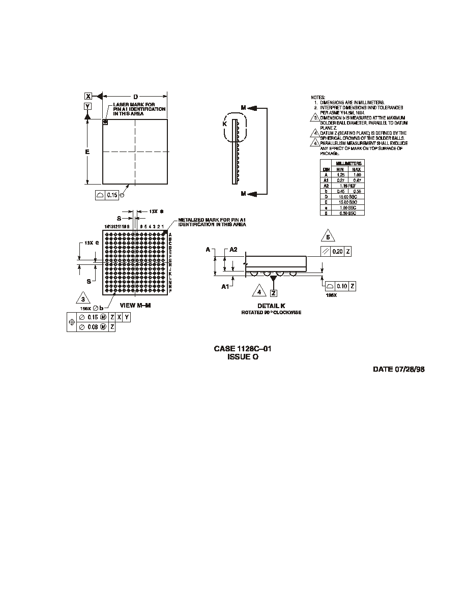
3-10
MAP-BGA Package Mechanical Drawing
3.3 MAP-BGA Package Mechanical Drawing
Figure 3-3. DSP56L307 Mechanical Information, 196-pin MAP-BGA Package

4-1
Chapter 4
Design
Considerations
4.1 Thermal Design Considerations
An estimate of the chip junction temperature, T
J
, in
∞
C can be obtained from
this equation:
Equation 1:
Where:
T
A
= ambient
temperature
∞C
R
JA
=
package junction-to-ambient thermal resistance ∞C/W
P
D
=
power dissipation in package
Historically, thermal resistance has been expressed as the sum of a
junction-to-case thermal resistance and a case-to-ambient thermal resistance,
as in this equation:
Equation 2:
Where:
R
JA
=
package junction-to-ambient thermal resistance ∞C/W
R
JC
=
package junction-to-case thermal resistance ∞C/W
R
CA
=
package case-to-ambient thermal resistance ∞C/W
R
JC
is device-related and cannot be influenced by the user. The user controls
the thermal environment to change the case-to-ambient thermal resistance,
R
CA
. For example, the user can change the air flow around the device, add a
heat sink, change the mounting arrangement on the printed circuit board
(PCB) or otherwise change the thermal dissipation capability of the area
surrounding the device on a PCB. This model is most useful for ceramic
packages with heat sinks; some 90 percent of the heat flow is dissipated
through the case to the heat sink and out to the ambient environment. For
ceramic packages, in situations where the heat flow is split between a path to
the case and an alternate path through the PCB, analysis of the device thermal
performance may need the additional modeling capability of a system-level
thermal simulation tool.
The thermal performance of plastic packages is more dependent on the
temperature of the PCB to which the package is mounted. Again, if the
estimates obtained from R
JA
do not satisfactorily answer whether the thermal
performance is adequate, a system-level model may be appropriate.
T
J
T
A
P
D
R
JA
◊
(
)
+
=
R
J A
R
JC
R
CA
+
=

4-2
Electrical Design Considerations
A complicating factor is the existence of three common ways to determine the junction-to-case thermal
resistance in plastic packages.
∑ To minimize temperature variation across the surface, the thermal resistance is measured from the
junction to the outside surface of the package (case) closest to the chip mounting area when that surface
has a proper heat sink.
∑ To define a value approximately equal to a junction-to-board thermal resistance, the thermal resistance
is measured from the junction to the point at which the leads attach to the case.
∑ If the temperature of the package case (T
T
) is determined by a thermocouple, thermal resistance is
computed from the value obtained by the equation (T
J
≠ T
T
)/P
D
.
As noted earlier, the junction-to-case thermal resistances quoted in this data sheet are determined using
the first definition. From a practical standpoint, that value is also suitable to determine the junction
temperature from a case thermocouple reading in forced convection environments. In natural convection,
the use of the junction-to-case thermal resistance to estimate junction temperature from a thermocouple
reading on the case of the package will yield an estimate of a junction temperature slightly higher than
actual temperature. Hence, the new thermal metric, thermal characterization parameter or
JT
, has been
defined to be (T
J
≠ T
T
)/P
D
. This value gives a better estimate of the junction temperature in natural
convection when the surface temperature of the package is used. Remember that surface temperature
readings of packages are subject to significant errors caused by inadequate attachment of the sensor to the
surface and to errors caused by heat loss to the sensor. The recommended technique is to attach a
40-gauge thermocouple wire and bead to the top center of the package with thermally conductive epoxy.
4.2 Electrical Design Considerations
CAUTION
This device contains protective circuitry to
guard against damage due to high static
voltage or electrical fields. However, normal
precautions are advised to avoid application
of any voltages higher than maximum rated
voltages to this high-impedance circuit.
Reliability of operation is enhanced if unused
inputs are tied to an appropriate logic voltage
level (for example, either GND or V
CC
).

4-3
Electrical Design Considerations
Use the following list of recommendations to ensure correct DSP operation.
∑ Provide a low-impedance path from the board power supply to each
V
CC
pin on the DSP and from the
board ground to each
GND
pin.
∑ Use at least six 0.01≠0.1
µ
F bypass capacitors positioned as close as possible to the four sides of the
package to connect the
V
CC
power source to
GND
.
∑ Ensure that capacitor leads and associated printed circuit traces that connect to the chip
V
CC
and
GND
pins are less than 0.5 inch per capacitor lead.
∑ Use at least a four-layer PCB with two inner layers for
V
CC
and
GND
.
∑ Because the DSP output signals have fast rise and fall times, PCB trace lengths should be minimal.
This recommendation particularly applies to the address and data buses as well as the
IRQA
,
IRQB
,
IRQC
,
IRQD
,
TA
, and
BG
pins. Maximum PCB trace lengths on the order of 6 inches are recommended.
∑ Consider all device loads as well as parasitic capacitance due to PCB traces when you calculate
capacitance. This is especially critical in systems with higher capacitive loads that could create higher
transient currents in the
V
CC
and
GND
circuits.
∑ All inputs must be terminated (that is, not allowed to float) by CMOS levels except for the three pins
with internal pull-up resistors (
TRST
,
TMS
,
DE
).
∑ Take special care to minimize noise levels on the
V
CCP
,
GND
P
, and
GND
P1
pins.
∑ The following pins must be asserted during power-up:
RESET
and
TRST
. A stable
EXTAL
signal
should be supplied before deassertion of
RESET
. If the V
CC
reaches the required level before EXTAL
is stable or other "required
RESET
duration" conditions are met (see Table 2-7), the device circuitry
can be in an uninitialized state that may result in significant power consumption and heat-up. Designs
should minimize this condition to the shortest possible duration.
∑ Ensure that during power-up, and throughout the DSP56L307 operation, V
CCQH
is always higher or
equal to the V
CC
voltage level.
∑ If multiple DSP devices are on the same board, check for cross-talk or excessive spikes on the supplies
due to synchronous operation of the devices.
∑ The Port A data bus (
D[0≠23]
), HI08, ESSI0, ESSI1, SCI, and timers all use internal keepers to
maintain the last output value even when the internal signal is tri-stated. Typically, no pull-up or
pull-down resistors should be used with these signal lines. However, if the DSP is connected to a
device that requires pull-up resistors (such as an MPC8260), the recommended resistor value is 10 K
or less. If more than one DSP must be connected in parallel to the other device, the pull-up resistor
value requirement changes as follows:
-- 2 DSPs = 7 K
or less
-- 3 DSPs = 4 K
or less
-- 4 DSPs = 3 K
or less
-- 5 DSPs = 2 K
or less
-- 6 DSPs = 1.5 K
or less

4-4
Power Consumption Considerations
4.3 Power Consumption Considerations
Power dissipation is a key issue in portable DSP applications. Some of the factors affecting current
consumption are described in this section. Most of the current consumed by CMOS devices is alternating
current (ac), which is charging and discharging the capacitances of the pins and internal nodes.
Current consumption is described by this formula:
Equation 3:
Where:
C =
node/pin
capacitance
V =
voltage
swing
f
=
frequency of node/pin toggle
Equation 4:
The maximum internal current (I
CCI
max) value reflects the typical possible switching of the internal
buses on best-case operation conditions--not necessarily a real application case. The typical internal
current (I
CCItyp
) value reflects the average switching of the internal buses on typical operating conditions.
Perform the following steps for applications that require very low current consumption:
1.
Set the EBD bit when you are not accessing external memory.
2.
Minimize external memory accesses, and use internal memory accesses.
3.
Minimize the number of pins that are switching.
4.
Minimize the capacitive load on the pins.
5.
Connect the unused inputs to pull-up or pull-down resistors.
6.
Disable unused peripherals.
7.
Disable unused pin activity (for example,
CLKOUT
,
XTAL
).
One way to evaluate power consumption is to use a current-per-MIPS measurement methodology to
minimize specific board effects (that is, to compensate for measured board current not caused by the
DSP). A benchmark power consumption test algorithm is listed in Appendix A. Use the test algorithm,
specific test current measurements, and the following equation to derive the current-per-MIPS value.
Equation 5:
Where:
I
typF2
=
current at F2
I
typF1
=
current at F1
F2
=
high frequency (any specified operating frequency)
F1
=
low frequency (any specified operating frequency lower than F2)
Note:
F1 should be significantly less than F2. For example, F2 could be 66 MHz and F1 could be 33
MHz. The degree of difference between F1 and F2 determines the amount of precision with
which the current rating can be determined for an application.
Example 4-1. Current Consumption
For a Port A address pin loaded with 50 pF capacitance, operating at 3.3 V, with a 66 MHz clock, toggling at its
maximum possible rate (33 MHz), the current consumption is expressed in Equation 4.
I
C
V
f
◊
◊
=
I
50
10
12
≠
◊
3.3
◊
33
◊
10
6
◊
5.48 mA
=
=
I MIPS
/
I MHz
/
I
typF2
I
typF1
≠
(
)
F2
F1
≠
(
)
/
=
=

4-5
PLL Performance Issues
4.4 PLL Performance Issues
The following explanations should be considered as general observations on expected PLL behavior.
There is no test that replicates these exact numbers. These observations were measured on a limited
number of parts and were not verified over the entire temperature and voltage ranges.
4.4.1 Phase Skew Performance
The phase skew of the PLL is defined as the time difference between the falling edges of
EXTAL
and
CLKOUT
for a given capacitive load on
CLKOUT
, over the entire process, temperature and voltage ranges.
As defined in Figure 2-2, External Clock Timing, on page 2-5 for input frequencies greater than 15 MHz
and the MF
4, this skew is greater than or equal to 0.0 ns and less than 1.8 ns; otherwise, this skew is
not guaranteed. However, for MF < 10 and input frequencies greater than 10 MHz, this skew is between
-
1.4 ns and +3.2 ns.
4.4.2 Phase Jitter Performance
The phase jitter of the PLL is defined as the variations in the skew between the falling edges of
EXTAL
and
CLKOUT
for a given device in specific temperature, voltage, input frequency, MF, and capacitive
load on
CLKOUT
. These variations are a result of the PLL locking mechanism. For input frequencies
greater than 15 MHz and MF
4, this jitter is less than
±
0.6 ns; otherwise, this jitter is not guaranteed.
However, for MF < 10 and input frequencies greater than 10 MHz, this jitter is less than
±
2 ns.
4.4.3 Frequency Jitter Performance
The frequency jitter of the PLL is defined as the variation of the frequency of
CLKOUT
. For small MF
(MF < 10) this jitter is smaller than 0.5 percent. For mid-range MF (10 < MF < 500) this jitter is between
0.5 percent and approximately 2 percent. For large MF (MF > 500), the frequency jitter is 2≠3 percent.
4.5 Input (EXTAL) Jitter Requirements
The allowed jitter on the frequency of
EXTAL
is 0.5 percent. If the rate of change of the frequency of
EXTAL
is slow (that is, it does not jump between the minimum and maximum values in one cycle) or the
frequency of the jitter is fast (that is, it does not stay at an extreme value for a long time), then the allowed
jitter can be 2 percent. The phase and frequency jitter performance results are valid only if the input jitter
is less than the prescribed values.

4-6
Input (EXTAL) Jitter Requirements

A-1
Appendix A
Power
Consumption
Benchmark
The following benchmark program evaluates DSP56L307 power use in a test situation. It enables the
PLL, disables the external clock, and uses repeated multiply-accumulate (MAC) instructions with a set of
synthetic DSP application data to emulate intensive sustained DSP operation.
;**************************************************************************
;**************************************************************************
;*
*
;* CHECKS Typical Power Consumption
*
;*
*
;**************************************************************************
page
200,55,0,0,0
nolist
I_VEC EQU $000000; Interrupt vectors for program debug only
START EQU $8000; MAIN (external) program starting address
INT_PROG EQU $100 ; INTERNAL program memory starting address
INT_XDAT EQU $0; INTERNAL X-data memory starting address
INT_YDAT EQU $0; INTERNAL Y-data memory starting address
INCLUDE "ioequ.asm"
INCLUDE "intequ.asm"
list
org
P:START
;
movep #$0243FF,x:M_BCR ;; BCR: Area 3 = 2 w.s (SRAM)
; Default: 2w.s (SRAM)
;
movep
#$0d0000,x:M_PCTL
; XTAL disable
; PLL enable
; CLKOUT disable
;
; Load the program
;
move
#INT_PROG,r0
move
#PROG_START,r1
do
#(PROG_END-PROG_START),PLOAD_LOOP
move
p:(r1)+,x0
move
x0,p:(r0)+
nop
PLOAD_LOOP
;
; Load the X-data
;
move
#INT_XDAT,r0
move
#XDAT_START,r1
do
#(XDAT_END-XDAT_START),XLOAD_LOOP
move
p:(r1)+,x0
move
x0,x:(r0)+
XLOAD_LOOP
;
; Load the Y-data
;
move
#INT_YDAT,r0
move
#YDAT_START,r1
do
#(YDAT_END-YDAT_START),YLOAD_LOOP
move
p:(r1)+,x0
move
x0,y:(r0)+
YLOAD_LOOP
;
jmp
INT_PROG
PROG_START
move
#$0,r0
move
#$0,r4
move
#$3f,m0
move
#$3f,m4
;
clr
a

A-2
Power Consumption Benchmark
clr
b
move
#$0,x0
move
#$0,x1
move
#$0,y0
move
#$0,y1
bset
#4,omr ;
ebd
;
sbr
dor
#60,_end
mac
x0,y0,a x:(r0)+,x1
y:(r4)+,y1
mac
x1,y1,a x:(r0)+,x0
y:(r4)+,y0
add
a,b
mac
x0,y0,a x:(r0)+,x1
mac
x1,y1,a
y:(r4)+,y0
move
b1,x:$ff
_end
bra
sbr
nop
nop
nop
nop
PROG_END
nop
nop
XDAT_START
;
org
x:0
dc
$262EB9
dc
$86F2FE
dc
$E56A5F
dc
$616CAC
dc
$8FFD75
dc
$9210A
dc
$A06D7B
dc
$CEA798
dc
$8DFBF1
dc
$A063D6
dc
$6C6657
dc
$C2A544
dc
$A3662D
dc
$A4E762
dc
$84F0F3
dc
$E6F1B0
dc
$B3829
dc
$8BF7AE
dc
$63A94F
dc
$EF78DC
dc
$242DE5
dc
$A3E0BA
dc
$EBAB6B
dc
$8726C8
dc
$CA361
dc
$2F6E86
dc
$A57347
dc
$4BE774
dc
$8F349D
dc
$A1ED12
dc
$4BFCE3
dc
$EA26E0
dc
$CD7D99
dc
$4BA85E
dc
$27A43F
dc
$A8B10C
dc
$D3A55
dc
$25EC6A
dc
$2A255B
dc
$A5F1F8
dc
$2426D1
dc
$AE6536
dc
$CBBC37
dc
$6235A4
dc
$37F0D
dc
$63BEC2
dc
$A5E4D3
dc
$8CE810
dc
$3FF09
dc
$60E50E
dc
$CFFB2F
dc
$40753C
dc
$8262C5
dc
$CA641A

A-3
Power Consumption Benchmark
dc
$EB3B4B
dc
$2DA928
dc
$AB6641
dc
$28A7E6
dc
$4E2127
dc
$482FD4
dc
$7257D
dc
$E53C72
dc
$1A8C3
dc
$E27540
XDAT_END
YDAT_START
;
org
y:0
dc
$5B6DA
dc
$C3F70B
dc
$6A39E8
dc
$81E801
dc
$C666A6
dc
$46F8E7
dc
$AAEC94
dc
$24233D
dc
$802732
dc
$2E3C83
dc
$A43E00
dc
$C2B639
dc
$85A47E
dc
$ABFDDF
dc
$F3A2C
dc
$2D7CF5
dc
$E16A8A
dc
$ECB8FB
dc
$4BED18
dc
$43F371
dc
$83A556
dc
$E1E9D7
dc
$ACA2C4
dc
$8135AD
dc
$2CE0E2
dc
$8F2C73
dc
$432730
dc
$A87FA9
dc
$4A292E
dc
$A63CCF
dc
$6BA65C
dc
$E06D65
dc
$1AA3A
dc
$A1B6EB
dc
$48AC48
dc
$EF7AE1
dc
$6E3006
dc
$62F6C7
dc
$6064F4
dc
$87E41D
dc
$CB2692
dc
$2C3863
dc
$C6BC60
dc
$43A519
dc
$6139DE
dc
$ADF7BF
dc
$4B3E8C
dc
$6079D5
dc
$E0F5EA
dc
$8230DB
dc
$A3B778
dc
$2BFE51
dc
$E0A6B6
dc
$68FFB7
dc
$28F324
dc
$8F2E8D
dc
$667842
dc
$83E053
dc
$A1FD90
dc
$6B2689
dc
$85B68E
dc
$622EAF
dc
$6162BC
dc
$E4A245
YDAT_END
;**************************************************************************

A-4
Power Consumption Benchmark
;
; EQUATES for DSP56L307 I/O registers and ports
;
; Last update: June 11 1995
;
;**************************************************************************
page
132,55,0,0,0
opt
mex
ioequ ident 1,0
;------------------------------------------------------------------------
;
; EQUATES for I/O Port Programming
;
;------------------------------------------------------------------------
; Register Addresses
M_HDR EQU $FFFFC9
; Host port GPIO data Register
M_HDDR EQU $FFFFC8
; Host port GPIO direction Register
M_PCRC EQU $FFFFBF
; Port C Control Register
M_PRRC EQU $FFFFBE
; Port C Direction Register
M_PDRC EQU $FFFFBD ; Port C GPIO Data Register
M_PCRD EQU $FFFFAF ; Port D Control register
M_PRRD EQU $FFFFAE ; Port D Direction Data Register
M_PDRD EQU $FFFFAD ; Port D GPIO Data Register
M_PCRE EQU $FFFF9F ; Port E Control register
M_PRRE EQU $FFFF9E ; Port E Direction Register
M_PDRE EQU $FFFF9D ; Port E Data Register
M_OGDB EQU $FFFFFC ; OnCE GDB Register
;------------------------------------------------------------------------
;
; EQUATES for Host Interface
;
;------------------------------------------------------------------------
; Register Addresses
M_HCR EQU $FFFFC2
; Host Control Register
M_HSR EQU $FFFFC3
; Host Status Register
M_HPCR EQU $FFFFC4
; Host Polarity Control Register
M_HBAR EQU $FFFFC5
; Host Base Address Register
M_HRX EQU $FFFFC6 ; Host Receive Register
M_HTX EQU $FFFFC7 ; Host Transmit Register
; HCR bits definition
M_HRIE EQU $0 ; Host Receive interrupts Enable
M_HTIE EQU $1 ; Host Transmit Interrupt Enable
M_HCIE EQU $2 ; Host Command Interrupt Enable
M_HF2 EQU $3 ; Host Flag 2
M_HF3 EQU $4 ; Host Flag 3
; HSR bits definition
M_HRDF EQU $0 ; Host Receive Data Full
M_HTDE EQU $1 ; Host Receive Data Empty
M_HCP EQU $2 ; Host Command Pending
M_HF0 EQU $3 ; Host Flag 0
M_HF1 EQU $4 ; Host Flag 1
; HPCR bits definition
M_HGEN EQU $0 ; Host Port GPIO Enable
M_HA8EN EQU $1 ; Host Address 8 Enable
M_HA9EN EQU $2 ; Host Address 9 Enable
M_HCSEN EQU $3 ; Host Chip Select Enable
M_HREN EQU $4 ; Host Request Enable
M_HAEN EQU $5
; Host Acknowledge Enable
M_HEN EQU $6 ; Host Enable
M_HOD EQU $8 ; Host Request Open Drain mode
M_HDSP EQU $9 ; Host Data Strobe Polarity
M_HASP EQU $A ; Host Address Strobe Polarity
M_HMUX EQU $B ; Host Multiplexed bus select
M_HD_HS EQU $C ; Host Double/Single Strobe select
M_HCSP EQU $D ; Host Chip Select Polarity
M_HRP EQU $E ; Host Request Polarity
M_HAP EQU $F ; Host Acknowledge Polarity

A-5
Power Consumption Benchmark
;------------------------------------------------------------------------
;
; EQUATES for Serial Communications Interface (SCI)
;
;------------------------------------------------------------------------
; Register Addresses
M_STXH EQU $FFFF97 ; SCI Transmit Data Register (high)
M_STXM EQU $FFFF96 ; SCI Transmit Data Register (middle)
M_STXL EQU $FFFF95 ; SCI Transmit Data Register (low)
M_SRXH EQU $FFFF9A ; SCI Receive Data Register (high)
M_SRXM EQU $FFFF99 ; SCI Receive Data Register (middle)
M_SRXL EQU $FFFF98 ; SCI Receive Data Register (low)
M_STXA EQU $FFFF94 ; SCI Transmit Address Register
M_SCR EQU $FFFF9C ; SCI Control Register
M_SSR EQU $FFFF93 ; SCI Status Register
M_SCCR EQU $FFFF9B ; SCI Clock Control Register
; SCI Control Register Bit Flags
M_WDS EQU $7 ; Word Select Mask (WDS0-WDS3)
M_WDS0 EQU 0 ; Word Select 0
M_WDS1 EQU 1 ; Word Select 1
M_WDS2 EQU 2 ; Word Select 2
M_SSFTD EQU 3
; SCI Shift Direction
M_SBK EQU 4 ; Send Break
M_WAKE EQU 5 ; Wakeup Mode Select
M_RWU EQU 6 ; Receiver Wakeup Enable
M_WOMS EQU 7 ; Wired-OR Mode Select
M_SCRE EQU 8 ; SCI Receiver Enable
M_SCTE EQU 9 ; SCI Transmitter Enable
M_ILIE EQU 10 ; Idle Line Interrupt Enable
M_SCRIE EQU 11 ; SCI Receive Interrupt Enable
M_SCTIE EQU 12 ; SCI Transmit Interrupt Enable
M_TMIE EQU 13 ; Timer Interrupt Enable
M_TIR EQU 14 ; Timer Interrupt Rate
M_SCKP EQU 15 ; SCI Clock Polarity
M_REIE EQU 16 ; SCI Error Interrupt Enable (REIE)
; SCI Status Register Bit Flags
M_TRNE EQU 0 ; Transmitter Empty
M_TDRE EQU 1 ; Transmit Data Register Empty
M_RDRF EQU 2 ; Receive Data Register Full
M_IDLE EQU 3 ; Idle Line Flag
M_OR EQU 4 ; Overrun Error Flag
M_PE EQU 5 ; Parity Error
M_FE EQU 6 ; Framing Error Flag
M_R8 EQU 7 ; Received Bit 8 (R8) Address
; SCI Clock Control Register
M_CD EQU $FFF ; Clock Divider Mask (CD0-CD11)
M_COD EQU 12 ; Clock Out Divider
M_SCP EQU 13 ; Clock Prescaler
M_RCM EQU 14 ; Receive Clock Mode Source Bit
M_TCM EQU 15 ; Transmit Clock Source Bit
;------------------------------------------------------------------------
;
; EQUATES for Synchronous Serial Interface (SSI)
;
;------------------------------------------------------------------------
;
; Register Addresses Of SSI0
M_TX00 EQU $FFFFBC ; SSI0 Transmit Data Register 0
M_TX01 EQU $FFFFBB ; SSIO Transmit Data Register 1
M_TX02 EQU $FFFFBA ; SSIO Transmit Data Register 2
M_TSR0 EQU $FFFFB9 ; SSI0 Time Slot Register
M_RX0 EQU $FFFFB8 ; SSI0 Receive Data Register
M_SSISR0 EQU $FFFFB7
; SSI0 Status Register
M_CRB0 EQU $FFFFB6 ; SSI0 Control Register B
M_CRA0 EQU $FFFFB5 ; SSI0 Control Register A
M_TSMA0 EQU $FFFFB4 ; SSI0 Transmit Slot Mask Register A
M_TSMB0 EQU $FFFFB3 ; SSI0 Transmit Slot Mask Register B
M_RSMA0 EQU $FFFFB2 ; SSI0 Receive Slot Mask Register A
M_RSMB0 EQU $FFFFB1 ; SSI0 Receive Slot Mask Register B

A-6
Power Consumption Benchmark
; Register Addresses Of SSI1
M_TX10 EQU $FFFFAC ; SSI1 Transmit Data Register 0
M_TX11 EQU $FFFFAB ; SSI1 Transmit Data Register 1
M_TX12 EQU $FFFFAA ; SSI1 Transmit Data Register 2
M_TSR1 EQU $FFFFA9 ; SSI1 Time Slot Register
M_RX1 EQU $FFFFA8 ; SSI1 Receive Data Register
M_SSISR1 EQU $FFFFA7
; SSI1 Status Register
M_CRB1 EQU $FFFFA6 ; SSI1 Control Register B
M_CRA1 EQU $FFFFA5 ; SSI1 Control Register A
M_TSMA1 EQU $FFFFA4 ; SSI1 Transmit Slot Mask Register A
M_TSMB1 EQU $FFFFA3 ; SSI1 Transmit Slot Mask Register B
M_RSMA1 EQU $FFFFA2 ; SSI1 Receive Slot Mask Register A
M_RSMB1 EQU $FFFFA1 ; SSI1 Receive Slot Mask Register B
; SSI Control Register A Bit Flags
M_PM EQU $FF ; Prescale Modulus Select Mask (PM0-PM7)
M_PSR EQU 11 ; Prescaler Range
M_DC EQU $1F000 ; Frame Rate Divider Control Mask (DC0-DC7)
M_ALC EQU 18
; Alignment Control (ALC)
M_WL EQU $380000 ; Word Length Control Mask (WL0-WL7)
M_SSC1 EQU 22 ; Select SC1 as TR #0 drive enable (SSC1)
; SSI Control Register B Bit Flags
M_OF EQU $3 ; Serial Output Flag Mask
M_OF0 EQU 0 ; Serial Output Flag 0
M_OF1 EQU 1 ; Serial Output Flag 1
M_SCD EQU $1C ; Serial Control Direction Mask
M_SCD0 EQU 2
; Serial Control 0 Direction
M_SCD1 EQU 3 ; Serial Control 1 Direction
M_SCD2 EQU 4 ; Serial Control 2 Direction
M_SCKD EQU 5 ; Clock Source Direction
M_SHFD EQU 6 ; Shift Direction
M_FSL EQU $180 ; Frame Sync Length Mask (FSL0-FSL1)
M_FSL0 EQU 7 ; Frame Sync Length 0
M_FSL1 EQU 8 ; Frame Sync Length 1
M_FSR EQU 9 ; Frame Sync Relative Timing
M_FSP EQU 10 ; Frame Sync Polarity
M_CKP EQU 11 ; Clock Polarity
M_SYN EQU 12 ; Sync/Async Control
M_MOD EQU 13 ; SSI Mode Select
M_SSTE EQU $1C000 ; SSI Transmit enable Mask
M_SSTE2 EQU 14 ; SSI Transmit #2 Enable
M_SSTE1 EQU 15 ; SSI Transmit #1 Enable
M_SSTE0 EQU 16 ; SSI Transmit #0 Enable
M_SSRE EQU 17 ; SSI Receive Enable
M_SSTIE EQU 18 ; SSI Transmit Interrupt Enable
M_SSRIE EQU 19 ; SSI Receive Interrupt Enable
M_STLIE EQU 20 ; SSI Transmit Last Slot Interrupt Enable
M_SRLIE EQU 21 ; SSI Receive Last Slot Interrupt Enable
M_STEIE EQU 22 ; SSI Transmit Error Interrupt Enable
M_SREIE EQU 23
; SI Receive Error Interrupt Enable
; SSI Status Register Bit Flags
M_IF EQU $3 ; Serial Input Flag Mask
M_IF0 EQU 0 ; Serial Input Flag 0
M_IF1 EQU 1 ; Serial Input Flag 1
M_TFS EQU 2 ; Transmit Frame Sync Flag
M_RFS EQU 3 ; Receive Frame Sync Flag
M_TUE EQU 4 ; Transmitter Underrun Error FLag
M_ROE EQU 5 ; Receiver Overrun Error Flag
M_TDE EQU 6 ; Transmit Data Register Empty
M_RDF EQU 7 ; Receive Data Register Full
; SSI Transmit Slot Mask Register A
M_SSTSA EQU $FFFF ; SSI Transmit Slot Bits Mask A (TS0-TS15)
; SSI Transmit Slot Mask Register B
M_SSTSB EQU $FFFF ; SSI Transmit Slot Bits Mask B (TS16-TS31)
; SSI Receive Slot Mask Register A
M_SSRSA EQU $FFFF ; SSI Receive Slot Bits Mask A (RS0-RS15)
; SSI Receive Slot Mask Register B
M_SSRSB EQU $FFFF ; SSI Receive Slot Bits Mask B (RS16-RS31)

A-7
Power Consumption Benchmark
;------------------------------------------------------------------------
;
; EQUATES for Exception Processing
;
;------------------------------------------------------------------------
; Register Addresses
M_IPRC EQU $FFFFFF ; Interrupt Priority Register Core
M_IPRP EQU $FFFFFE ; Interrupt Priority Register Peripheral
; Interrupt Priority Register Core (IPRC)
M_IAL EQU $7 ; IRQA Mode Mask
M_IAL0 EQU 0 ; IRQA Mode Interrupt Priority Level (low)
M_IAL1 EQU 1 ; IRQA Mode Interrupt Priority Level (high)
M_IAL2 EQU 2 ; IRQA Mode Trigger Mode
M_IBL EQU $38 ; IRQB Mode Mask
M_IBL0 EQU 3 ; IRQB Mode Interrupt Priority Level (low)
M_IBL1 EQU 4 ; IRQB Mode Interrupt Priority Level (high)
M_IBL2 EQU 5 ; IRQB Mode Trigger Mode
M_ICL EQU $1C0 ; IRQC Mode Mask
M_ICL0 EQU 6 ; IRQC Mode Interrupt Priority Level (low)
M_ICL1 EQU 7 ; IRQC Mode Interrupt Priority Level (high)
M_ICL2 EQU 8 ; IRQC Mode Trigger Mode
M_IDL EQU $E00 ; IRQD Mode Mask
M_IDL0 EQU 9 ; IRQD Mode Interrupt Priority Level (low)
M_IDL1 EQU 10 ; IRQD Mode Interrupt Priority Level (high)
M_IDL2 EQU 11 ; IRQD Mode Trigger Mode
M_D0L EQU $3000 ; DMA0 Interrupt priority Level Mask
M_D0L0 EQU 12 ; DMA0 Interrupt Priority Level (low)
M_D0L1 EQU 13 ; DMA0 Interrupt Priority Level (high)
M_D1L EQU $C000 ; DMA1 Interrupt Priority Level Mask
M_D1L0 EQU 14 ; DMA1 Interrupt Priority Level (low)
M_D1L1 EQU 15 ; DMA1 Interrupt Priority Level (high)
M_D2L EQU $30000 ; DMA2 Interrupt priority Level Mask
M_D2L0 EQU 16 ; DMA2 Interrupt Priority Level (low)
M_D2L1 EQU 17 ; DMA2 Interrupt Priority Level (high)
M_D3L EQU $C0000 ; DMA3 Interrupt Priority Level Mask
M_D3L0 EQU 18 ; DMA3 Interrupt Priority Level (low)
M_D3L1 EQU 19 ; DMA3 Interrupt Priority Level (high)
M_D4L EQU $300000 ; DMA4 Interrupt priority Level Mask
M_D4L0 EQU 20 ; DMA4 Interrupt Priority Level (low)
M_D4L1 EQU 21 ; DMA4 Interrupt Priority Level (high)
M_D5L EQU $C00000 ; DMA5 Interrupt priority Level Mask
M_D5L0 EQU 22 ; DMA5 Interrupt Priority Level (low)
M_D5L1 EQU 23 ; DMA5 Interrupt Priority Level (high)
; Interrupt Priority Register Peripheral (IPRP)
M_HPL EQU $3 ; Host Interrupt Priority Level Mask
M_HPL0 EQU 0 ; Host Interrupt Priority Level (low)
M_HPL1 EQU 1 ; Host Interrupt Priority Level (high)
M_S0L EQU $C ; SSI0 Interrupt Priority Level Mask
M_S0L0 EQU 2 ; SSI0 Interrupt Priority Level (low)
M_S0L1 EQU 3 ; SSI0 Interrupt Priority Level (high)
M_S1L EQU $30 ; SSI1 Interrupt Priority Level Mask
M_S1L0 EQU 4 ; SSI1 Interrupt Priority Level (low)
M_S1L1 EQU 5 ; SSI1 Interrupt Priority Level (high)
M_SCL EQU $C0 ; SCI Interrupt Priority Level Mask
M_SCL0 EQU 6 ; SCI Interrupt Priority Level (low)
M_SCL1 EQU 7 ; SCI Interrupt Priority Level (high)
M_T0L EQU $300 ; TIMER Interrupt Priority Level Mask
M_T0L0 EQU 8 ; TIMER Interrupt Priority Level (low)
M_T0L1 EQU 9 ; TIMER Interrupt Priority Level (high)
;------------------------------------------------------------------------
;
; EQUATES for TIMER
;
;------------------------------------------------------------------------
; Register Addresses Of TIMER0
M_TCSR0 EQU $FFFF8F ; Timer 0 Control/Status Register

A-8
Power Consumption Benchmark
M_TLR0 EQU $FFFF8E
; TIMER0 Load Reg
M_TCPR0 EQU $FFFF8D ; TIMER0 Compare Register
M_TCR0 EQU $FFFF8C
; TIMER0 Count Register
; Register Addresses Of TIMER1
M_TCSR1 EQU $FFFF8B
; TIMER1 Control/Status Register
M_TLR1 EQU $FFFF8A
; TIMER1 Load Reg
M_TCPR1 EQU $FFFF89 ; TIMER1 Compare Register
M_TCR1 EQU $FFFF88
; TIMER1 Count Register
; Register Addresses Of TIMER2
M_TCSR2 EQU $FFFF87 ; TIMER2 Control/Status Register
M_TLR2 EQU $FFFF86
; TIMER2 Load Reg
M_TCPR2 EQU $FFFF85
; TIMER2 Compare Register
M_TCR2 EQU $FFFF84
; TIMER2 Count Register
M_TPLR EQU $FFFF83
; TIMER Prescaler Load Register
M_TPCR EQU $FFFF82
; TIMER Prescalar Count Register
; Timer Control/Status Register Bit Flags
M_TE EQU 0
; Timer Enable
M_TOIE EQU 1
; Timer Overflow Interrupt Enable
M_TCIE EQU 2
; Timer Compare Interrupt Enable
M_TC EQU $F0
; Timer Control Mask (TC0-TC3)
M_INV EQU 8
; Inverter Bit
M_TRM EQU 9
; Timer Restart Mode
M_DIR EQU 11
; Direction Bit
M_DI EQU 12
; Data Input
M_DO EQU 13
; Data Output
M_PCE EQU 15
; Prescaled Clock Enable
M_TOF EQU 20
; Timer Overflow Flag
M_TCF EQU 21
; Timer Compare Flag
; Timer Prescaler Register Bit Flags
M_PS EQU $600000
; Prescaler Source Mask
M_PS0 EQU 21
M_PS1 EQU 22
;
Timer Control Bits
M_TC0 EQU 4
; Timer Control 0
M_TC1 EQU 5
; Timer Control 1
M_TC2 EQU 6
; Timer Control 2
M_TC3 EQU 7
; Timer Control 3
;------------------------------------------------------------------------
;
; EQUATES for Direct Memory Access (DMA)
;
;------------------------------------------------------------------------
; Register Addresses Of DMA
M_DSTR EQU FFFFF4
; DMA Status Register
M_DOR0 EQU $FFFFF3 ; DMA Offset Register 0
M_DOR1 EQU $FFFFF2 ; DMA Offset Register 1
M_DOR2 EQU $FFFFF1 ; DMA Offset Register 2
M_DOR3 EQU $FFFFF0 ; DMA Offset Register 3
; Register Addresses Of DMA0
M_DSR0 EQU $FFFFEF ; DMA0 Source Address Register
M_DDR0 EQU $FFFFEE ; DMA0 Destination Address Register
M_DCO0 EQU $FFFFED ; DMA0 Counter
M_DCR0 EQU $FFFFEC ; DMA0 Control Register
; Register Addresses Of DMA1
M_DSR1 EQU $FFFFEB ; DMA1 Source Address Register
M_DDR1 EQU $FFFFEA ; DMA1 Destination Address Register
M_DCO1 EQU $FFFFE9 ; DMA1 Counter
M_DCR1 EQU $FFFFE8 ; DMA1 Control Register
; Register Addresses Of DMA2
M_DSR2 EQU $FFFFE7 ; DMA2 Source Address Register

A-9
Power Consumption Benchmark
M_DDR2 EQU $FFFFE6 ; DMA2 Destination Address Register
M_DCO2 EQU $FFFFE5 ; DMA2 Counter
M_DCR2 EQU $FFFFE4 ; DMA2 Control Register
; Register Addresses Of DMA4
M_DSR3 EQU $FFFFE3 ; DMA3 Source Address Register
M_DDR3 EQU $FFFFE2 ; DMA3 Destination Address Register
M_DCO3 EQU $FFFFE1 ; DMA3 Counter
M_DCR3 EQU $FFFFE0 ; DMA3 Control Register
; Register Addresses Of DMA4
M_DSR4 EQU $FFFFDF ; DMA4 Source Address Register
M_DDR4 EQU $FFFFDE ; DMA4 Destination Address Register
M_DCO4 EQU $FFFFDD ; DMA4 Counter
M_DCR4 EQU $FFFFDC ; DMA4 Control Register
; Register Addresses Of DMA5
M_DSR5 EQU $FFFFDB ; DMA5 Source Address Register
M_DDR5 EQU $FFFFDA ; DMA5 Destination Address Register
M_DCO5 EQU $FFFFD9 ; DMA5 Counter
M_DCR5 EQU $FFFFD8 ; DMA5 Control Register
;
DMA Control Register
M_DSS EQU $3
; DMA Source Space Mask (DSS0-Dss1)
M_DSS0 EQU 0
; DMA Source Memory space 0
M_DSS1 EQU 1
; DMA Source Memory space 1
M_DDS EQU $C
; DMA Destination Space Mask (DDS-DDS1)
M_DDS0 EQU 2
; DMA Destination Memory Space 0
M_DDS1 EQU 3
; DMA Destination Memory Space 1
M_DAM EQU $3f0 ; DMA Address Mode Mask (DAM5-DAM0)
M_DAM0 EQU 4
; DMA Address Mode 0
M_DAM1 EQU 5
; DMA Address Mode 1
M_DAM2 EQU 6
; DMA Address Mode 2
M_DAM3 EQU 7
; DMA Address Mode 3
M_DAM4 EQU 8
; DMA Address Mode 4
M_DAM5 EQU 9
; DMA Address Mode 5
M_D3D EQU 10
; DMA Three Dimensional Mode
M_DRS EQU $F800; DMA Request Source Mask (DRS0-DRS4)
M_DCON EQU 16
; DMA Continuous Mode
M_DPR EQU $60000; DMA Channel Priority
M_DPR0 EQU 17
; DMA Channel Priority Level (low)
M_DPR1 EQU 18
; DMA Channel Priority Level (high)
M_DTM EQU $380000; DMA Transfer Mode Mask (DTM2-DTM0)
M_DTM0 EQU 19
; DMA Transfer Mode 0
M_DTM1 EQU 20
; DMA Transfer Mode 1
M_DTM2 EQU 21
; DMA Transfer Mode 2
M_DIE EQU 22
; DMA Interrupt Enable bit
M_DE EQU 23
; DMA Channel Enable bit
; DMA Status Register
M_DTD EQU $3F
; Channel Transfer Done Status MASK (DTD0-DTD5)
M_DTD0 EQU 0
; DMA Channel Transfer Done Status 0
M_DTD1 EQU 1
; DMA Channel Transfer Done Status 1
M_DTD2 EQU 2
; DMA Channel Transfer Done Status 2
M_DTD3 EQU 3
; DMA Channel Transfer Done Status 3
M_DTD4 EQU 4
; DMA Channel Transfer Done Status 4
M_DTD5 EQU 5
; DMA Channel Transfer Done Status 5
M_DACT EQU 8
; DMA Active State
M_DCH EQU $E00; DMA Active Channel Mask (DCH0-DCH2)
M_DCH0 EQU 9
; DMA Active Channel 0
M_DCH1 EQU 10 ; DMA Active Channel 1
M_DCH2 EQU 11 ; DMA Active Channel 2
;------------------------------------------------------------------------
;
; EQUATES for Enhanced Filter Co-Processor (EFCOP)
;
;------------------------------------------------------------------------
M_FDIR EQU $FFFFB0 ; EFCOP Data Input Register
M_FDOR EQU $FFFFB1 ; EFCOP Data Output Register
M_FKIR EQU $FFFFB2 ; EFCOP K-Constant Register
M_FCNT EQU $FFFFB3 ; EFCOP Filter Counter
M_FCSR EQU $FFFFB4 ; EFCOP Control Status Register
M_FACR EQU $FFFFB5 ; EFCOP ALU Control Register

A-10
Power Consumption Benchmark
M_FDBA EQU $FFFFB6 ; EFCOP Data Base Address
M_FCBA EQU $FFFFB7 ; EFCOP Coefficient Base Address
M_FDCH EQU $FFFFB8 ; EFCOP Decimation/Channel Register
;------------------------------------------------------------------------
;
; EQUATES for Phase Locked Loop (PLL)
;
;------------------------------------------------------------------------
; Register Addresses Of PLL
M_PCTL EQU $FFFFFD ; PLL Control Register
; PLL Control Register
M_MF EQU $FFF : Multiplication Factor Bits Mask (MF0-MF11)
M_DF EQU $7000 ; Division Factor Bits Mask (DF0-DF2)
M_XTLR EQU 15 ; XTAL Range select bit
M_XTLD EQU 16 ; XTAL Disable Bit
M_PSTP EQU 17 ; STOP Processing State Bit
M_PEN EQU 18
; PLL Enable Bit
M_PCOD EQU 19 ; PLL Clock Output Disable Bit
M_PD EQU $F00000; PreDivider Factor Bits Mask (PD0-PD3)
;------------------------------------------------------------------------
;
; EQUATES for BIU
;
;------------------------------------------------------------------------
; Register Addresses Of BIU
M_BCR EQU $FFFFFB; Bus Control Register
M_DCR EQU $FFFFFA; DRAM Control Register
M_AAR0 EQU $FFFFF9; Address Attribute Register 0
M_AAR1 EQU $FFFFF8; Address Attribute Register 1
M_AAR2 EQU $FFFFF7; Address Attribute Register 2
M_AAR3 EQU $FFFFF6; Address Attribute Register 3
M_IDR EQU $FFFFF5 ; ID Register
; Bus Control Register
M_BA0W EQU $1F ; Area 0 Wait Control Mask (BA0W0-BA0W4)
M_BA1W EQU $3E0; Area 1 Wait Control Mask (BA1W0-BA14)
M_BA2W EQU $1C00; Area 2 Wait Control Mask (BA2W0-BA2W2)
M_BA3W EQU $E000; Area 3 Wait Control Mask (BA3W0-BA3W3)
M_BDFW EQU $1F0000 ; Default Area Wait Control Mask (BDFW0-BDFW4)
M_BBS EQU 21
; Bus State
M_BLH EQU 22
; Bus Lock Hold
M_BRH EQU 23
; Bus Request Hold
; DRAM Control Register
M_BCW EQU $3
; In Page Wait States Bits Mask (BCW0-BCW1)
M_BRW EQU $C
; Out Of Page Wait States Bits Mask (BRW0-BRW1)
M_BPS EQU $300 ; DRAM Page Size Bits Mask (BPS0-BPS1)
M_BPLE EQU 11
; Page Logic Enable
M_BME EQU 12
; Mastership Enable
M_BRE EQU 13
; Refresh Enable
M_BSTR EQU 14
; Software Triggered Refresh
M_BRF EQU $7F8000; Refresh Rate Bits Mask (BRF0-BRF7)
M_BRP EQU 23
; Refresh prescaler
; Address Attribute Registers
M_BAT EQU $3
; Ext. Access Type and Pin Def. Bits Mask (BAT0-BAT1)
M_BAAP EQU 2
; Address Attribute Pin Polarity
M_BPEN EQU 3
; Program Space Enable
M_BXEN EQU 4
; X Data Space Enable
M_BYEN EQU 5
; Y Data Space Enable
M_BAM EQU 6
; Address Muxing
M_BPAC EQU 7
; Packing Enable
M_BNC EQU $F00 ; Number of Address Bits to Compare Mask (BNC0-BNC3)
M_BAC EQU $FFF000; Address to Compare Bits Mask (BAC0-BAC11)

A-11
Power Consumption Benchmark
; control and status bits in SR
M_CP EQU $c00000; mask for CORE-DMA priority bits in SR
M_CA EQU 0
; Carry
M_V EQU 1
; Overflow
M_Z EQU 2
; Zero
M_N EQU 3
; Negative
M_U EQU 4
; Unnormalized
M_E EQU 5
; Extension
M_L EQU 6
; Limit
M_S EQU 7
; Scaling Bit
M_I0 EQU 8
; Interupt Mask Bit 0
M_I1 EQU 9
; Interupt Mask Bit 1
M_S0 EQU 10
; Scaling Mode Bit 0
M_S1 EQU 11
; Scaling Mode Bit 1
M_SC EQU 13
; Sixteen_Bit Compatibility
M_DM EQU 14
; Double Precision Multiply
M_LF EQU 15
; DO-Loop Flag
M_FV EQU 16
; DO-Forever Flag
M_SA EQU 17
; Sixteen-Bit Arithmetic
M_CE EQU 19
; Instruction Cache Enable
M_SM EQU 20
; Arithmetic Saturation
M_RM EQU 21
; Rounding Mode
M_CP0 EQU 22
; bit 0 of priority bits in SR
M_CP1 EQU 23
; bit 1 of priority bits in SR
; control and status bits in OMR
M_CDP EQU $300 ; mask for CORE-DMA priority bits in OMR
M_MA equ0
; Operating Mode A
M_MB equ1
; Operating Mode B
M_MC equ2
; Operating Mode C
M_MD equ3
; Operating Mode D
M_EBD EQU 4
; External Bus Disable bit in OMR
M_SD EQU 6
; Stop Delay
M_MS EQU 7
; Memory Switch bit in OMR
M_CDP0 EQU 8
; bit 0 of priority bits in OMR
M_CDP1 EQU 9
; bit 1 of priority bits in OMR
M_BEN EQU 10 ; Burst Enable
M_TAS EQU 11 ; TA Synchronize Select
M_BRT EQU 12
; Bus Release Timing
M_ATE EQU 15
; Address Tracing Enable bit in OMR.
M_XYS EQU 16
; Stack Extension space select bit in OMR.
M_EUN EQU 17
; Extensed stack UNderflow flag in OMR.
M_EOV EQU 18
; Extended stack OVerflow flag in OMR.
M_WRP EQU 19
; Extended WRaP flag in OMR.
M_SEN EQU 20
; Stack Extension Enable bit in OMR.
;*************************************************************************
;
; EQUATES for DSP56L307 interrupts
;
; Last update: June 11 1995
;
;*************************************************************************
page
132,55,0,0,0
opt
mex
intequ ident 1,0
if
@DEF(I_VEC)
;leave user definition as is.
else
I_VEC EQU $0
endif
;------------------------------------------------------------------------
; Non-Maskable interrupts
;------------------------------------------------------------------------
I_RESET EQU I_VEC+$00
; Hardware RESET
I_STACK EQU I_VEC+$02
; Stack Error
I_ILL EQU I_VEC+$04
; Illegal Instruction
I_DBG EQU I_VEC+$06
; Debug Request
I_TRAP EQU I_VEC+$08
; Trap

A-12
Power Consumption Benchmark
I_NMI EQU I_VEC+$0A
; Non Maskable Interrupt
;------------------------------------------------------------------------
; Interrupt Request Pins
;------------------------------------------------------------------------
I_IRQA EQU I_VEC+$10 ; IRQA
I_IRQB EQU I_VEC+$12
; IRQB
I_IRQC EQU I_VEC+$14
; IRQC
I_IRQD EQU I_VEC+$16
; IRQD
;------------------------------------------------------------------------
; DMA Interrupts
;------------------------------------------------------------------------
I_DMA0 EQU I_VEC+$18
; DMA Channel 0
I_DMA1 EQU I_VEC+$1A ; DMA Channel 1
I_DMA2 EQU I_VEC+$1C ; DMA Channel 2
I_DMA3 EQU I_VEC+$1E ; DMA Channel 3
I_DMA4 EQU I_VEC+$20 ; DMA Channel 4
I_DMA5 EQU I_VEC+$22 ; DMA Channel 5
;------------------------------------------------------------------------
; Timer Interrupts
;------------------------------------------------------------------------
I_TIM0C EQU I_VEC+$24
; TIMER 0 compare
I_TIM0OF EQU I_VEC+$26 ; TIMER 0 overflow
I_TIM1C EQU I_VEC+$28
; TIMER 1 compare
I_TIM1OF EQU I_VEC+$2A ; TIMER 1 overflow
I_TIM2C EQU I_VEC+$2C
; TIMER 2 compare
I_TIM2OF EQU I_VEC+$2E ; TIMER 2 overflow
;------------------------------------------------------------------------
; ESSI Interrupts
;------------------------------------------------------------------------
I_SI0RD EQU I_VEC+$30
; ESSI0 Receive Data
I_SI0RDE EQU I_VEC+$32 ; ESSI0 Receive Data w/ exception Status
I_SI0RLS EQU I_VEC+$34 ; ESSI0 Receive last slot
I_SI0TD EQU I_VEC+$36 ; ESSI0 Transmit data
I_SI0TDE EQU I_VEC+$38 ; ESSI0 Transmit Data w/ exception Status
I_SI0TLS EQU I_VEC+$3A ; ESSI0 Transmit last slot
I_SI1RD EQU I_VEC+$40
; ESSI1 Receive Data
I_SI1RDE EQU I_VEC+$42 ; ESSI1 Receive Data w/ exception Status
I_SI1RLS EQU I_VEC+$44 ; ESSI1 Receive last slot
I_SI1TD EQU I_VEC+$46 ; ESSI1 Transmit data
I_SI1TDE EQU I_VEC+$48 ; ESSI1 Transmit Data w/ exception Status
I_SI1TLS EQU I_VEC+$4A ; ESSI1 Transmit last slot
;------------------------------------------------------------------------
; SCI Interrupts
;------------------------------------------------------------------------
I_SCIRD EQU I_VEC+$50 ; SCI Receive Data
I_SCIRDE EQU I_VEC+$52 ; SCI Receive Data With Exception Status
I_SCITD EQU I_VEC+$54 ; SCI Transmit Data
I_SCIIL EQU I_VEC+$56 ; SCI Idle Line
I_SCITM EQU I_VEC+$58 ; SCI Timer
;------------------------------------------------------------------------
; HOST Interrupts
;------------------------------------------------------------------------
I_HRDF EQU I_VEC+$60 ; Host Receive Data Full
I_HTDE EQU I_VEC+$62 ; Host Transmit Data Empty
I_HC EQU I_VEC+$64
; Default Host Command
;-----------------------------------------------------------------------
; EFCOP Filter Interrupts
;-----------------------------------------------------------------------
I_FDIIE EQU I_VEC+$68 ; EFilter input buffer empty
I_FDOIE EQU I_VEC+$6A ; EFilter output buffer full
;------------------------------------------------------------------------
; INTERRUPT ENDING ADDRESS
;------------------------------------------------------------------------
I_INTEND EQU I_VEC+$FF ; last address of interrupt vector space

Index
Index-1
A
ac electrical characteristics 2-4
address bus 1-1
applications iv
B
benchmark test algorithm A-1
block diagram i
bootstrap ROM iii
Boundary Scan (JTAG Port) timing diagram 2-48
bus
address 1-2
control 1-1
data 1-2
external address 1-5
external data 1-5
multiplexed 1-2
non-multiplexed 1-2
C
clock 1-1
,
1-4
external 2-4
clocks
internal 2-4
crystal oscillator circuits 2-5
D
data bus 1-1
data memory expansion iv
Data Strobe (DS) 1-2
dc electrical characteristics 2-3
DE
signal 1-18
Debug Event signal (
DE
signal) 1-18
Debug mode
entering 1-18
external indication 1-18
Debug support iii
design considerations
electrical 4-2
,
4-3
PLL 4-5
power consumption 4-4
thermal 4-1
documentation list v
Double Data Strobe 1-2
DRAM
controller iv
out of page
read access 2-23
wait states selection guide 2-20
write access 2-24
Page mode
read accesses 2-19
wait states selection guide 2-16
write accesses 2-19
refresh access 2-24
DSP56300
Family Manual v
DSP56L307
block diagram i
Technical Data v
User's Manual v
E
EFCOP
interrupts A-12
electrical
design considerations 4-2
,
4-3
Enhanced Synchronous Serial Interface (ESSI) iii
,
1-1
,
1-2
,
1-13
,
1-14
receiver timing 2-43
transmitter timing 2-42
ESSI
timings 2-38
,
2-40
external address bus 1-5
external bus control 1-5
,
1-6
,
1-7
external clock operation 2-4
external data bus 1-5
external interrupt timing (negative
edge-triggered) 2-10
external level-sensitive fast interrupt timing 2-9
external memory access (DMA Source)
timing 2-11
External Memory Expansion Port 2-11
external memory expansion port 1-5
F
functional groups 1-2
functional signal groups 1-1
G
General-Purpose Input/Output (GPIO) iii
,
1-2
ground 1-1
,
1-3
PLL 1-3
H
Host Interface (HI08) iii
,
1-1
,
1-2
,
1-9
,
1-10
,
1-11
,
1-12
Host Port Control Register (HPCR) 1-10
,
1-12
host port

Index
Index-2
configuration 1-9
usage considerations 1-9
Host Port Control Register (HPCR) 1-10
,
1-12
Host Request
Double 1-2
Single 1-2
Host Request (HR) 1-2
I
information sources v
instruction cache iii
internal clocks 2-4
interrupt and mode control 1-1
,
1-8
interrupt control 1-8
interrupt timing 2-7
external level-sensitive fast 2-9
external negative edge-triggered 2-10
interrupts
EFCOP A-12
J
Joint Test Action Group (JTAG)
interface 1-18
JTAG iii
JTAG Port
reset timing diagram 2-48
timing 2-48
JTAG/OnCE Interface signals
Debug Event signal (
DE
signal) 1-18
JTAG/OnCE port 1-1
,
1-2
K
keeper circuit
design considerations 4-3
M
MAP-BGA
ball grid drawing (bottom) 3-3
ball grid drawing (top) 3-2
mechanical drawing 3-10
maximum ratings 2-1
,
2-2
memory expansion port iii
mode control 1-8
Mode select timing 2-7
multiplexed bus 1-2
multiplexed bus timings
read 2-34
write 2-35
N
non-multiplexed bus 1-2
non-multiplexed bus timings
read 2-32
write 2-33
O
off-chip memory iii
OnCE module iii
Debug request 2-49
on-chip DRAM controller iv
On-Chip Emulation (OnCE) module
interface 1-18
On-Chip Emulation module iii
on-chip memory iii
operating mode select timing 2-10
ordering information Back Cover
P
package
MAP-BGA description 3-2
,
3-3
,
3-10
Phase-Lock Loop (PLL) 1-1
,
2-6
design considerations 4-5
performance issues 4-5
PLL 1-4
Port A 1-1
,
1-5
,
2-11
Port B 1-1
,
1-2
,
1-11
Port C 1-1
,
1-2
,
1-13
Port D 1-1
,
1-2
,
1-14
Port E 1-1
power 1-1
,
1-2
,
1-3
power consumption
design considerations 4-4
power consumption benchmark test A-1
power management iv
program memory expansion iv
program RAM iii
R
recovery from Stop state using IRQA 2-10
RESET 1-8
reset
clock signals 1-4
interrupt signals 1-8
JTAG signals 1-18
mode control 1-8
OnCE signals 1-18
PLL signals 1-4
Reset timing 2-7
,
2-9
ROM, bootstrap iii

Index
Index-3
S
Serial Communication Interface (SCI) iii
,
1-1
,
1-2
,
1-16
Asynchronous mode timing 2-37
Synchronous mode timing 2-37
signal groupings 1-1
signals 1-1
functional grouping 1-2
Single Data Strobe 1-2
SRAM
read access 2-15
support iv
write access 2-15
Stop mode iv
Stop state
recovery from 2-10
Stop timing 2-7
supply voltage 2-2
Switch mode iii
synchronous bus timings
SRAM
2 wait states 2-27
SRAM 1 wait state (BCR controlled) 2-26
T
target applications iv
Test Access Port (TAP) iii
timing diagram 2-48
Test Clock (TCLK) input timing diagram 2-47
thermal
design considerations 4-1
Timer
event input restrictions 2-44
Timers 1-1
,
1-2
,
1-17
interrupt generation 2-44
,
2-45
timing
ESSI 2-38
W
Wait mode iv
World Wide Web v
X
X-data RAM iii
Y
Y-data RAM iii

Index
Index-4

DSP56L307/D, REV. 3
HOW TO REACH US:
USA / EUROPE / Locations Not Listed:
Motorola Literature Distribution
P.O. Box 5405
Denver, Colorado 80217
1-800-521-6274 or 480-768-2130
JAPAN:
Motorola Japan Ltd.
SPS, Technical Information Center
3-20-1, Minami-Azabu Minato-ku
Tokyo 106-8573 Japan
81-3-3440-3569
ASIA/PACIFIC:
Motorola Semiconductors H.K. Ltd.
Silicon Harbour Centre
2 Dai King Street
Tai Po Industrial Estate,
Tai Po, N.T., Hong Kong
852-26668334
HOME PAGE:
http://motorola.com/semiconductors/
Information in this document is provided solely to enable system and software implementers to use
Motorola products. There are no express or implied copyright licenses granted hereunder to design or
fabricate any integrated circuits or integrated circuits based on the information in this document.
Motorola reserves the right to make changes without further notice to any products herein. Motorola
makes no warranty, representation or guarantee regarding the suitability of its products for any
particular purpose, nor does Motorola assume any liability arising out of the application or use of any
product or circuit, and specifically disclaims any and all liability, including without limitation
consequential or incidental damages. "Typical" parameters that may be provided in Motorola data
sheets and/or specifications can and do vary in different applications and actual performance may
vary over time. All operating parameters, including "Typicals" must be validated for each customer
application by customer's technical experts. Motorola does not convey any license under its patent
rights nor the rights of others. Motorola products are not designed, intended, or authorized for use as
components in systems intended for surgical implant into the body, or other applications intended to
support or sustain life, or for any other application in which the failure of the Motorola product could
create a situation where personal injury or death may occur. Should Buyer purchase or use Motorola
products for any such unintended or unauthorized application, Buyer shall indemnify and hold
Motorola and its officers, employees, subsidiaries, affiliates, and distributors harmless against all
claims, costs, damages, and expenses, and reasonable attorney fees arising out of, directly or
indirectly, any claim of personal injury or death associated with such unintended or unauthorized use,
even if such claim alleges that Motorola was negligent regarding the design or manufacture of the part.
MOTOROLA and the Stylized M Logo are registered in the U.S. Patent and Trademark Office. OnCE
and digital dna are trademarks of Motorola, Inc. All other product or service names are the property
of their respective owners. Motorola, Inc. is an Equal Opportunity/Affirmative Action Employer.
© Motorola, Inc. 2001, 2003
Ordering Information
Consult a Motorola Semiconductor sales office or authorized distributor to determine product availability and place an order.
Part
Supply
Voltage
Package Type
Pin
Count
Core
Frequency
(MHz)
Order Number
DSP56L307
1.8 V core
3.3 V I/O
Molded Array Process-Ball Grid Array (MAP-BGA)
196
160
DSP56L307VF160