
Order this document by
MC68HC812A4EC/D
© MOTOROLA INC, 1997, 1998
SEMICONDUCTOR
MOTOROLA
TECHNICAL DATA
PRELIMINARY
7/28/98
Technical Supplement
MC68C812A4 3.3V Electrical Characteristics
The MC68C812A4 is the low-voltage version of the standard MC68HC812A4 microcontroller unit
(MCU), a 16-bit device composed of standard on-chip peripheral modules connected by an intermodule
bus. Modules include a 16-bit central processing unit (CPU12), a Lite integration module (LIM), two
asynchronous serial communications interfaces (SCI0 and SCI1), a serial peripheral interface (SPI), a
timer and pulse accumulation module, an 8-bit analog-to-digital converter (ATD), 1-Kbyte RAM, 4-Kbyte
EEPROM, and memory expansion logic with chip selects, key wakeup ports, and a phase-locked loop
(PLL).
This supplement contains the most accurate electrical information for the MC68C812A4 microcontroller
available at the time of publication. The information should be considered preliminary and is subject to
change. The following characteristics are contained in this document:
Table 1 Maximum Ratings
Table 2 Thermal Characteristics
Table 3 DC Electrical Characteristics
Table 4 Supply Current
Table 5 ATD Maximum Ratings
Table 6 ATD DC Electrical Characteristics
Table 7 Analog Converter Characteristics (Operating)
Table 8 ATD AC Characteristics (Operating)
Table 9 EEPROM Characteristics
Table 10 Control Timing
Table 11 Peripheral Port Timing
Table 12 Non-Multiplexed Expansion Bus Timing
Table 13 SPI Timing
MOTOROLA
MC68C812A4
2
PRELIMINARY
NOTES:
1. Permanent damage can occur if maximum ratings are exceeded. Exposures to voltages or cur-
rents in excess of recommended values affects device reliability. Device modules may not operate
normally while being exposed to electrical extremes.
2. Refer to MC68HC812A4TS/D Technical Summary for complete part numbers.
3. One pin at a time, observing maximum power dissipation limits. Internal circuitry protects the in-
puts against damage caused by high static voltages or electric fields; however, normal precautions
are necessary to avoid application of any voltage higher than maximum-rated voltages to this high-
impedance circuit. Extended operation at the maximum ratings can adversely affect device reli-
ability. Tying unused inputs to an appropriate logic voltage level (either GND or V
DD
) enhances
reliability of operation.
NOTES:
1. This is an approximate value, neglecting P
I/O
.
2. For most applications P
I/O
´ P
INT
and can be neglected.
3. K is a constant pertaining to the device. Solve for K with a known T
A
and a measured P
D
(at equilibrium). Use
this value of K to solve for P
D
and T
J
iteratively for any value of T
A
.
Table 1 Maximum Ratings
1
Rating
Symbol
Value
Unit
Supply voltage
V
DD
,
V
DDA
,
V
DDX
-
0.3 to
+
6.5
V
Input voltage
V
IN
-
0.3 to
+
6.5
V
Operating temperature range
2
MC68C812A4PV5
T
A
T
L
to T
H
0 to
+
70
∞
C
Storage temperature range
T
stg
-
55 to
+
150
∞
C
Current drain per pin
3
Excluding V
DD
and V
SS
I
IN
±
25
mA
V
DD
differential voltage
V
DD
-
V
DDX
6.5
V
Table 2 Thermal Characteristics
Characteristic
Symbol
Value
Unit
Average junction temperature
T
J
T
A
+
(P
D
◊
JA
)
∞
C
Ambient temperature
T
A
User-determined
∞
C
Package thermal resistance (junction-to-ambient)
112-pin thin quad flat pack (TQFP)
JA
39
∞
C/W
Total power dissipation
1
P
D
P
INT
+
P
I/O
or
W
Device internal power dissipation
P
INT
I
DD
◊
V
DD
W
I/O pin power dissipation
2
P
I/O
User-determined
W
A constant
3
K
P
D
◊
(T
A
+
273
∞
C)
+
JA
◊
P
D
2
W ∑
∞
C
K
T
J
273
∞
C
+
--------------------------

MC68C812A4
MOTOROLA
3
PRELIMINARY
NOTES:
1. Specification is for parts in the 0 to
+
70
∞
C range. Higher temperature ranges will result in increased current
leakage.
Table 3 DC Electrical Characteristics
V
DD
=
3.3 Vdc
±
0.3V, V
SS
=
0 Vdc, T
A
=
T
L
to T
H
, unless otherwise noted
Characteristic
Symbol
Min
Max
Unit
Input high voltage, all inputs
V
IH
0.7
◊
V
DD
V
DD
+
0.3
V
Input low voltage, all inputs
V
IL
V
SS
-
0.3
0.2
◊
V
DD
V
Output high voltage
All I/O and output pins
Normal drive strength
I
OH
=
-
10.0
µ
A
I
OH
=
-
0.8 mA
Reduced drive strength
I
OH
=
-
4.0
µ
A
I
OH
=
-
0.3 mA
V
OH
V
DD
-
0.2
V
DD
-
0.8
V
DD
-
0.2
V
DD
-
0.8
--
--
--
--
V
V
V
V
Output low voltage, All I/O and output pins, normal drive strength
I
OL
=
10.0
µ
A
I
OL
=
1.6 mA
EXTAL, PAD[7:0], V
RH
, V
RL
, V
FP
, XIRQ, reduced drive strength
I
OL
=
3.6
µ
A
I
OL
=
0.6 mA
V
OL
--
--
--
--
V
SS
+
0.2
V
SS
+
0.4
V
SS
+
0.2
V
SS
+
0.4
V
V
V
V
Input leakage current
1
all inputs except IRQ, PAD7, and XFC
V
in
=
V
DD
or V
SS
IRQ, PAD7, XFC
I
in
--
--
±
1
±
10
µ
A
µ
A
Three-state leakage, I/O ports, BKGD, and RESET
I
OZ
--
±
2.5
µ
A
Input capacitance
All input pins and ATD pins (non-sampling)
ATD pins (sampling)
All I/O pins
C
in
--
--
--
10
15
20
pF
pF
pF
Output load capacitance
All outputs except PS[7:4]
PS[7:4]
C
L
--
--
90
130
pF
pF
Active pull-up, pull-down current
IRQ, XIRQ, ECLK, LSTRB, R/W , BKGD, MODA, MODB, ARST
Ports A, B, C, D, F, G, H, J, S, T
I
APU
50
500
µ
A
RAM standby voltage, power down
V
SB
2.0
--
V
RAM standby current
I
SB
--
1
mA

MOTOROLA
MC68C812A4
4
PRELIMINARY
Note: I
DD
is tested with a rail-to-rail square wave on EXTAL
NOTES:
1. Includes I
DD
and I
DDA
.
Table 4 Supply Current
V
DD
=
3.3 Vdc
±
0.3V, V
SS
=
0 Vdc, T
A
=
T
L
to T
H
, unless otherwise noted
Characteristic
Symbol
4 MHz
5 MHz
Unit
Maximum total supply current
RUN:
Single-chip mode
Expanded mode
I
DD
15
21
17
25
mA
mA
WAIT: (All peripheral functions shut down)
Single-chip mode
Expanded mode
W
IDD
3
3
3.5
3.5
mA
mA
STOP:
Single-chip mode, no clocks
S
IDD
250
250
µ
A
Maximum power dissipation
1
Single-chip mode
Expanded mode
P
D
54
76
62
90
mW
mW
Table 5 ATD Maximum Ratings
Characteristic
Symbol
Value
Units
ATD reference voltage
V
RH
V
DDA
V
RL
V
SSA
V
RH
V
RL
-
0.3 to
+
6.5
-
0.3 to
+
6.5
V
V
V
SS
differential voltage
|
V
SS
-
V
SSA
|
0.1
V
V
DD
differential voltage
|
V
DD
-
V
DDA
|
V
DD
-
V
DDX
6.5
6.5
V
V
V
REF
differential voltage
|
V
RH
-
V
RL
|
6.5
V
Reference to supply differential voltage
|
V
RH
-
V
DDA
|
|
V
RL
-
V
SSA
|
6.5
6.5
V
V
MC68C812A4
MOTOROLA
5
PRELIMINARY
NOTES:
1. Accuracy is guaranteed at V
RH
-
V
RL
=
3.3 Vdc
±
0.3V
.
2. To obtain full-scale, full-range results, V
SSA
V
RL
V
INDC
V
RH
V
DDA
.
3. Maximum leakage occurs at maximum operating temperature. Current decreases by ap-
proximately one-half for each 10
∞
C decrease from maximum temperature.
Table 6 ATD DC Electrical Characteristics
V
DD
=
3.3 Vdc
±
0.3V, V
SS
=
0 Vdc, T
A
=
T
L
to T
H
, ATD Clock
=
2 MHz, unless
otherwise noted
Characteristic
Symbol Min
Max
Unit
Analog supply voltage
V
DDA
3.0
3.6
V
Analog supply current
Normal operation
I
DDA
1.0
mA
Reference voltage, low
V
RL
V
SSA
V
DDA
/
2
V
Reference voltage, high
V
RH
V
DDA
/
2
V
DDA
V
V
REF
differential reference voltage
1
V
RH
-
V
RL
3.0
3.6
V
Input voltage
2
V
INDC
V
SSA
V
DDA
V
Input current, off channel
3
I
OFF
100
nA
Reference supply current
I
REF
250
µ
A
Input capacitance
Not Sampling
Sampling
C
INN
C
INS
10
15
pF
pF

MOTOROLA
MC68C812A4
6
PRELIMINARY
NOTES:
1. V
RH
-
V
RL
3.072V
2. At V
REF
=
3.072V, one 8-bit count = 12 mV.
3. Eight-bit absolute error of 2 counts (24 mV) includes 1/2 count (6 mV) inherent quantization error and 1 1/2
counts (18 mV) circuit (differential, integral, and offset) error.
4. Maximum source impedance is application-dependent. Error resulting from pin leakage depends on junction
leakage into the pin and on leakage due to charge-sharing with internal capacitance.
Error from junction leakage is a function of external source impedance and input leakage current. Expected error
in result value due to junction leakage is expressed in voltage (V
ERRJ
):
V
ERRJ
=
R
S
◊
I
OFF
where I
OFF
is a function of operating temperature. Charge-sharing effects with internal capacitors are a function of
ATD clock speed, the number of channels being scanned, and source impedance. For 8-bit conversions, charge
pump leakage is computed as follows:
V
ERRJ
=
.25pF
◊
V
DDA
◊
R
S
◊
ATDCLK/(8
◊
number of channels)
Table 7 Analog Converter Characteristics (Operating)
V
DD
=
3.3 Vdc
±
0.3V, V
SS
=
0 Vdc, T
A
=
T
L
to T
H
, ATD Clock
=
2 MHz, unless otherwise noted
Characteristic
Symbol
Min
Typical
Max
Unit
8-bit resolution
1
2 counts
24
mV
Differential non-linearity
2
DNL
-
0.5
+
0.5
count
Integral non-linearity
2
INL
-
1
+
1
count
Absolute error
2,3
2, 4, 8, and 16 ATD sample clocks
AE
-
2
+
2
count
Maximum source impedance
R
S
20
See note
4
K
Table 8 ATD AC Characteristics (Operating)
V
DD
=
3.3 Vdc
±
0.3V, V
SS
=
0 Vdc, T
A
=
T
L
to T
H
, ATD Clock
=
2 MHz, unless
otherwise noted
Characteristic
Symbol Min
Max
Unit
ATD operating clock frequency
f
ATDCLK
0.5
2.0
MHz
Conversion time per channel
0.5 MHz
f
ATDCLK
2 MHz
18 ATD clocks
32 ATD clocks
t
CONV
9.0
16.0
32.0
60.0
µ
s
µ
s
Stop recovery time
V
DDA
=
3.3V
t
SR
50
µ
s
MC68C812A4
MOTOROLA
7
PRELIMINARY
NOTES:
1. RC oscillator must be enabled if programming is desired and f
SYS
<
f
PROG
.
Table 9 EEPROM Characteristics
V
DD
=
3.3 Vdc
±
0.3V, V
SS
=
0 Vdc, T
A
=
T
L
to T
H
, unless otherwise noted
Characteristic
Symbol Min
Typical
Max
Unit
Minimum programming clock frequency
1
f
PROG
3.0
MHz
Programming time
t
PROG
20
ms
Clock recovery time following STOP, to continue programming
t
CRSTOP
t
PROG
+
1
ms
Erase time
t
ERASE
20
ms
Write/erase endurance
10,000
30,000
cycles
Data retention
10
years
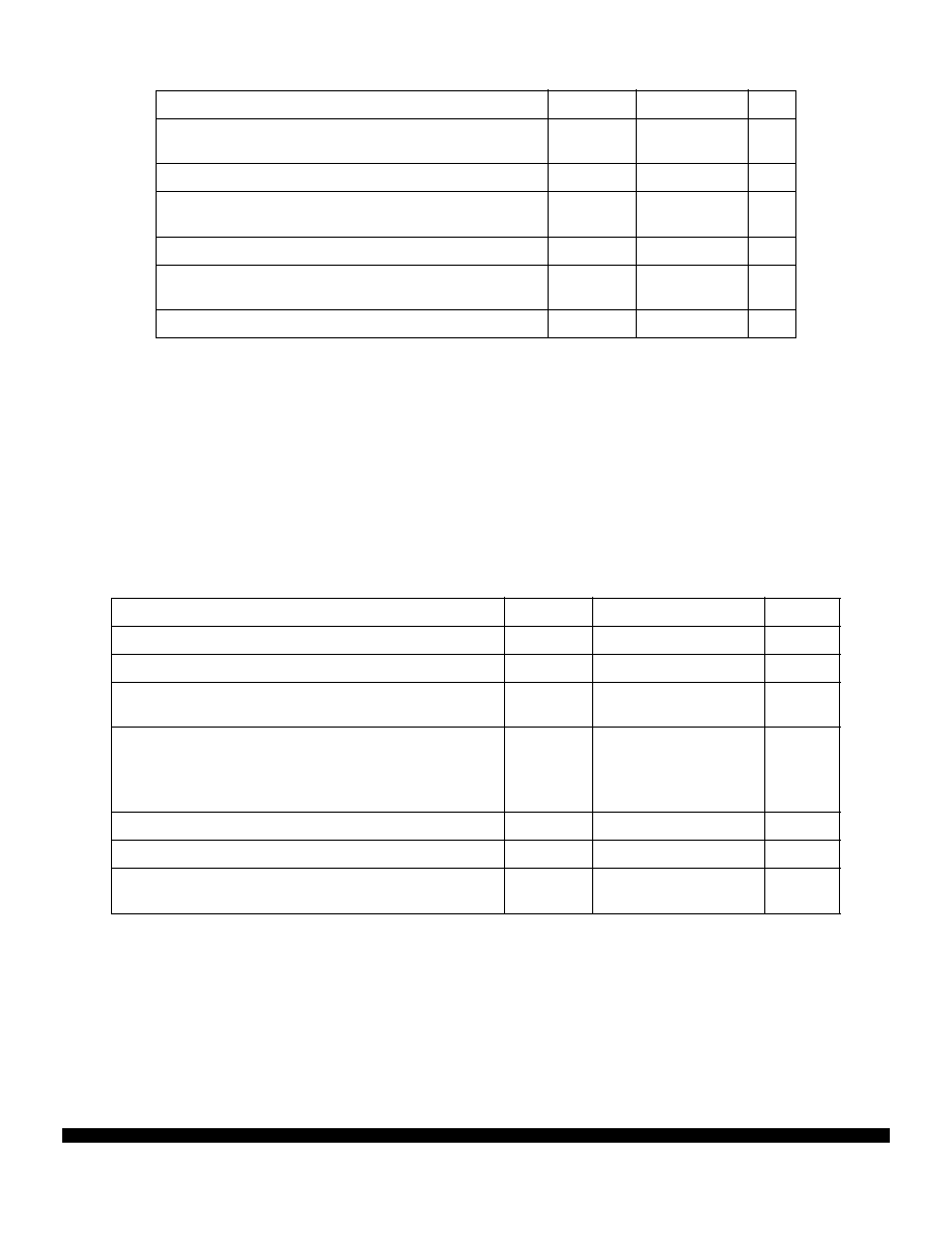
Table 10 Control Timing
Characteristic
Symbol 5.0
MHz
Unit
Min
Max
Frequency of operation
f
o
dc
5.0
MHz
E-clock period
t
cyc
200
--
ns
Crystal frequency
f
XTAL
--
10.0
MHz
External oscillator frequency
2f
o
dc
10.0
MHz
Processor control setup time
t
PCSU
=
t
cyc
/
2
+
30
t
PCSU
130
--
ns
Reset input pulse width
To guarantee external reset vector
Minimum input time (can be preempted by internal reset)
PW
RSTL
32
2
--
--
t
cyc
t
cyc
Mode programming setup time
t
MPS
4
--
t
cyc
Mode programming hold time
t
MPH
10
--
ns
Interrupt pulse width, IRQ, edge-sensitive mode, KWU
PW
IRQ
=
2t
cyc
+
20
PW
IRQ
420
--
ns
Wait recovery startup time
t
WRS
--
4
t
cyc
Timer pulse width, input capture pulse accumulator input
PW
TIM
=
2t
cyc
+
20
PW
TIM
420
--
ns

MOTOROLA
MC68C812A4
8
PRELIMINARY
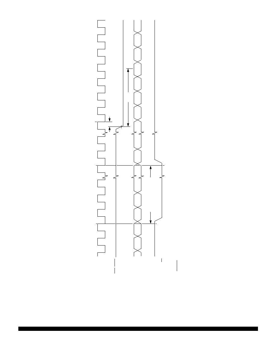
Figure 1 Timer Inputs
PT7
2
PT7
1
PT[7:0]
2
PT[7:0]
1
TIMER INPUT TIMING
NOTES
:
1. Rising edge sensitive input
2. Falling edge sensitive input
PW
TIM
PW
PA

MC68C812A4
MOTOROLA
9
PRELIMINARY
Figure 2 POR and External Reset Timing Diagram
t
PCSU
INTERNAL
MODA, MODB
ECLK
EXTAL
V
DD
RESET
4098 t
cyc
FREE
FFFE
FFFE
3RD
1ST
2ND
FREE
FFFE
FFFE
FFFE
t
MPH
PW
RSTL
t
MPS
POR EXT RESET TIM
ADDRESS
PIPE
PIPE
PIPE
1ST EXEC
3RD
PIPE
2ND PIPE
1ST PIPE
1ST EXEC
NOTE: Reset timing is subject to change.
MOTOROLA
MC68C812A4
10
PRELIMINARY
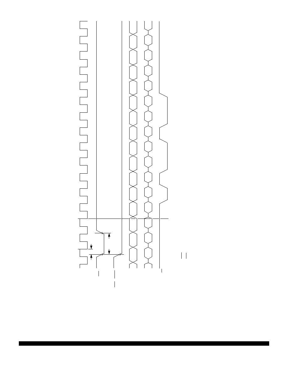
Figure 3 STOP Recovery Timing Diagram
PW
IRQ
t
STOPDELAY
3
IRQ
1
IRQ
or XIRQ
ECLK
1ST
ADDRESS
4
SP-9
FREE
FREE
VECTOR
FREE
FREE
Resume program with instruction which follows the STOP instruction.
I
NTERNAL
ADDRESS
5
STOP RECOVERY TIM
CLOCKS
NOTES:
1. Edge Sensitive
IRQ
pin (IRQE bit = 1)
2. Level sensitive
IRQ
pin (IRQE bit = 0)
3. t
STOPDELAY
= 4098 t
cyc
if DLY bit = 1 or 2 t
cyc
if DLY = 0.
4. XIRQ
with X bit in CCR = 1.
5. IRQ
or (
XIRQ
with X bit in CCR = 0).
OPT
1ST
2ND
3RD
1ST
EXEC
PIPE
PIPE
EXEC
SP-8
SP-6
FETCH
PIPE
SP-6
SP-8
SP-9
MC68C812A4
MOTOROLA
11
PRELIMINARY
Figure 4 WAIT Recovery Timing Diagram
WAIT RECOVERY TIM
t
PCSU
PC, IY, IX, B:A, , CCR
STACK REGISTERS
ECLK
R/
W
ADDRESS
IRQ
, XIRQ
,
OR INTERNAL
INTERRUPTS
SP ≠ 2
SP ≠ 4
SP ≠
6
.
.
.
SP ≠ 9
SP ≠ 9
SP ≠ 9
.
.
.
SP ≠ 9
SP ≠ 9
VECTOR
FREE
1ST
2ND
3RD
PIPE
t
WRS
NOTE: RESET
also causes recovery from WAIT.
ADDRESS
PIPE
PIPE
1ST
EXEC
MOTOROLA
MC68C812A4
12
PRELIMINARY
Figure 5 Interrupt Timing Diagram
INTERRUPT TIM
ECLK
PW
IRQ
1ST
3RD
ADDRESS
IR
Q
1
SP ≠ 9
t
PCSU
IRQ
2
, XIRQ
,
OR INTERNAL
INTERRUPT
VECTOR
SP ≠ 2
1ST
SP ≠ 4
SP ≠ 6
2ND
SP ≠ 8
DATA
VECT
PC
IY
IX
B:A
CCR
PROG
R/
W
NOTES:
1. Edge sensitive
IRQ
pin (IRQE bit = 1)
2. Level sensitive
IRQ
pin (IRQE bit = 0)
FETCH
ADDR
EXEC
PIPE
PIPE
PIPE
PROG
FETCH
PROG
FETCH
MC68C812A4
MOTOROLA
13
PRELIMINARY
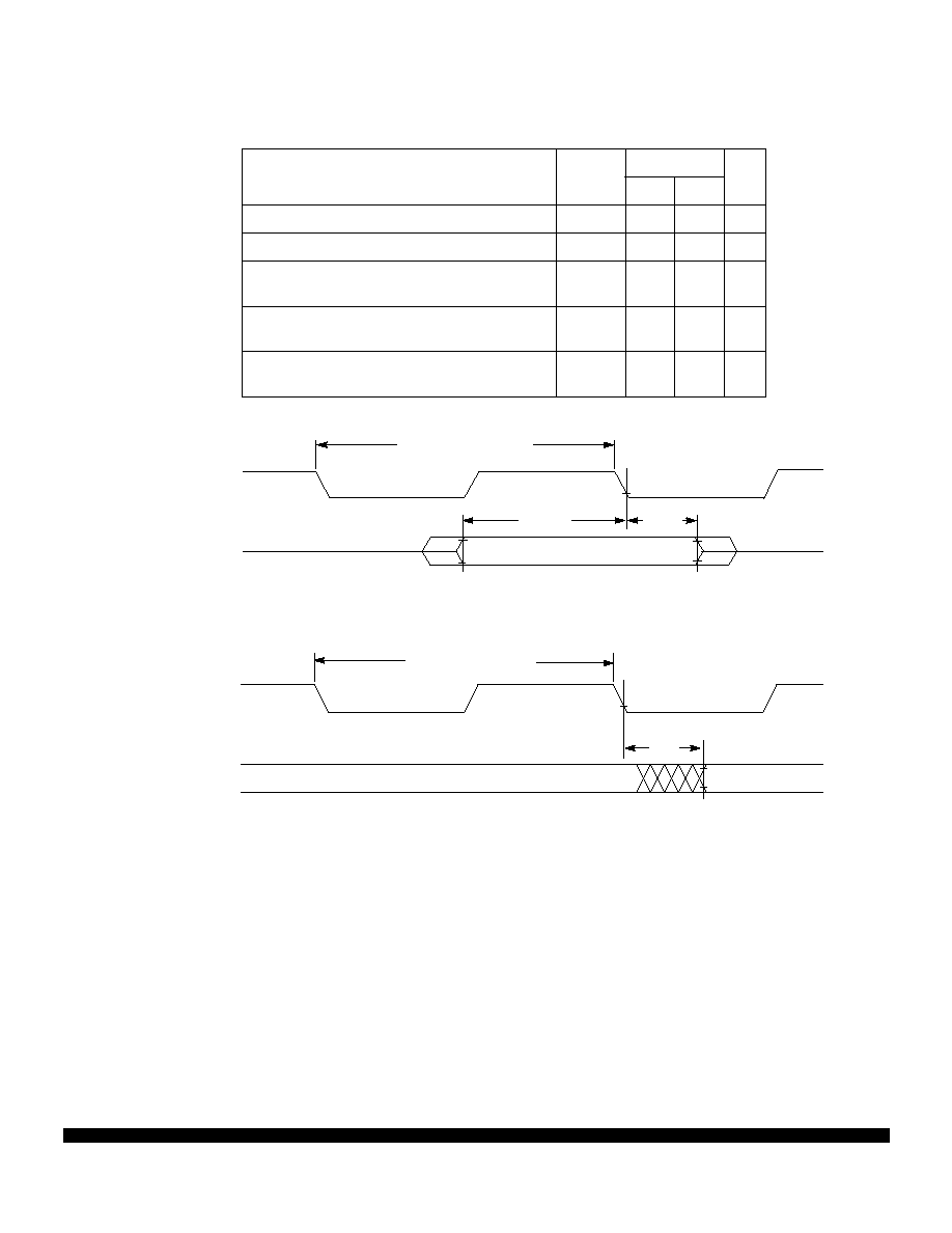
Figure 6 Port Read Timing Diagram
Figure 7 Port Write Timing Diagram
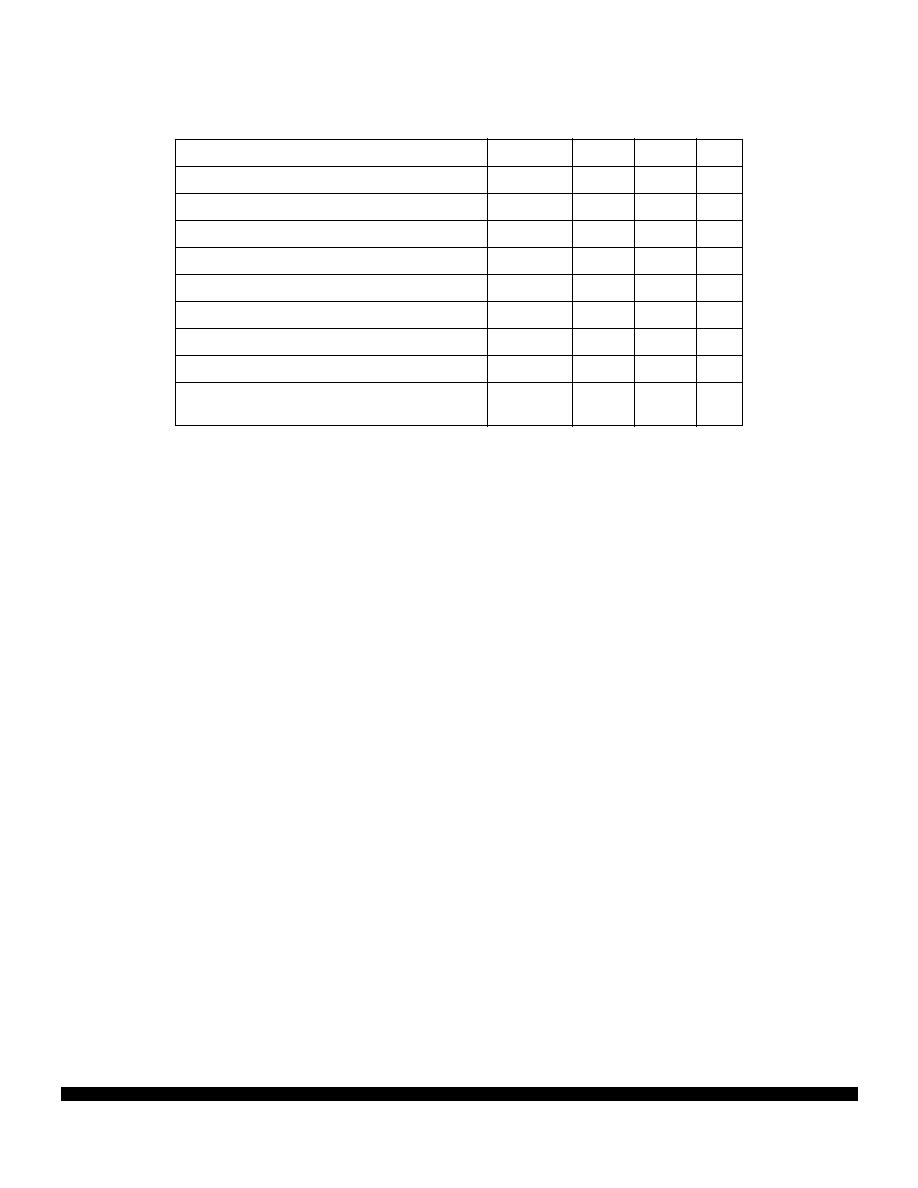
Table 11 Peripheral Port Timing
Characteristic
Symbol 5.0
MHz
Unit
Min
Max
Frequency of operation (E-clock frequency)
f
o
dc
5.0
MHz
E-clock period
t
cyc
200
--
ns
Peripheral data setup time
MCU read of ports
t
PDSU
=
t
cyc
/
2
+
30
t
PDSU
130
--
ns
Peripheral data hold time
MCU read of ports
t
PDH
0
--
ns
Delay time, peripheral data write
MCU write to ports
t
PWD
--
40
ns
PORT RD TIM
ECLK
MCU READ OF PORT
PORTS
t
PDSU
t
PDH
PORT WR TIM
ECLK
MCU WRITE TO PORT
PREVIOUS PORT DATA
NEW DATA VALID
PORT A
t
PWD
MOTOROLA
MC68C812A4
14
PRELIMINARY
NOTES:
1. All timings are calculated for normal port drives.
2. This characteristic is affected by clock stretch.
Add N
◊
t
cyc
where N = 0, 1, 2, or 3, depending on the number of clock stretches.
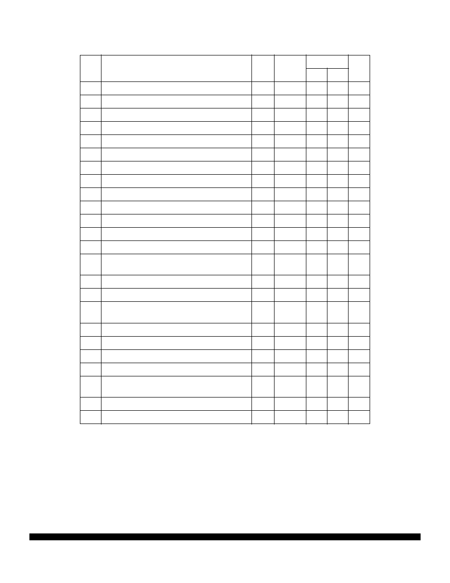
Table 12 Non-Multiplexed Expansion Bus Timing
V
DD
=
3.3 Vdc
±
0.3V, V
SS
=
0 Vdc, T
A
=
T
L
to T
H
, unless otherwise noted
Num
Characteristic
1
Delay
Symbol
5 MHz
Unit
Min
Max
Frequency of operation (E-clock frequency)
f
o
dc
5.0
MHz
1
Cycle time
t
cyc
=
1
/
f
o
t
cyc
200
--
ns
2
Pulse width, E low
PW
EL
=
t
cyc
/
2
+
delay
-
2
PW
EL
98
--
ns
3
Pulse width, E high
2
PW
EH
=
t
cyc
/
2
+
delay
-
2
PW
EH
98
--
ns
5
Address delay time
t
AD
=
t
cyc
/
4
+
delay
29
t
AD
--
79
ns
6
Address hold time
--
t
AH
20
--
ns
7
Address valid time to E rise
t
AV
=
PW
EL
-
t
AD
--
t
AV
28
--
ns
11
Read data setup time
--
t
DSR
30
--
ns
12
Read data hold time
--
t
DHR
0
--
ns
13
Write data delay time
t
DDW
=
t
cyc
/
4
+
delay
25
t
DDW
--
75
ns
14
Write data hold time
--
t
DHW
20
--
ns
15
Write data setup time
2
t
DSW
=
PW
EH
-
t
DDW
--
t
DSW
23
--
ns
16
Read/write delay time
t
RWD
=
t
cyc
/
4
+
delay
20
t
RWD
--
70
ns
17
Read/write valid time to E rise
t
RWV
=
PW
EL
-
t
RWD
--
t
RWV
28
--
ns
18
Read/write hold time
--
t
RWH
20
--
ns
19
Low strobe delay time
t
LSD
=
t
cyc
/
4
+
delay
20
t
LSD
--
70
ns
20
Low strobe valid time to E rise
t
LSV
=
PW
EL
-
t
LSD
--
t
LSV
28
--
ns
21
Low strobe hold time
--
t
LSH
20
--
ns
22
Address access time
2
t
ACCA
=
t
cyc
-
t
AD
-
t
DSR
--
t
ACCA
--
100
ns
23
Access time from E rise
2
t
ACCE
=
PW
EH
-
t
DSR
--
t
ACCE
--
68
ns
26
Chip select delay time
t
CSD
=
t
cyc
/
4
+
delay
29
t
CSD
--
79
ns
27
Chip select access time
2
t
ACCS
=
t
cyc
-
t
CSD
-
t
DSR
--
t
ACCS
--
100
ns
28
Chip select hold time
--
t
CSH
0
10
ns
29
Chip select negated time
t
CSN
=
t
cyc
/
4
+
delay
5
t
CSN
55
--
ns
MC68C812A4
MOTOROLA
15
PRELIMINARY
Figure 8 Non-Multiplexed Expansion Bus Timing Diagram
ECLK
R/W
1
6
DATA[15:0]
DATA[15:0]
2
3
18
22
11
12
13
14
ADDR[15:0]
NOTE: Measurement points shown are 20% and 70% of V
DD
5
15
BUS TIM
CS
16
27
28
17
READ
WRITE
23
LSTRB
21
19
20
(W/O TAG ENABLED)
26
29
7

MOTOROLA
MC68C812A4
16
PRELIMINARY
NOTES:
1. All AC timing is shown with respect to 20% V
DD
and 70% V
DD
levels unless otherwise noted.
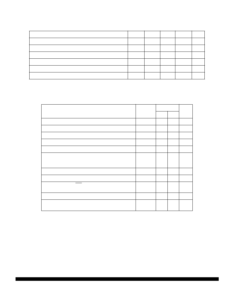
Table 13 SPI Timing
V
DD
=
3.3 Vdc
±
0.3V
, V
SS
=
0 Vdc, T
A
=
T
L
to T
H
, 130 pF load on all SPI pins
1
Num
Function
Symbol
Min
Max
Unit
Operating Frequency
Master
Slave
f
op
DC
DC
1
/
2
1
/
2
E-clock
frequency
1
SCK Period
Master
Slave
t
sck
2
2
256
--
t
cyc
t
cyc
2
Enable Lead Time
Master
Slave
t
lead
1
/
2
1
--
--
t
sck
t
cyc
3
Enable Lag Time
Master
Slave
t
lag
1
/
2
1
--
--
t
sck
t
cyc
4
Clock (SCK) High or Low Time
Master
Slave
t
wsck
t
cyc
-
60
t
cyc
-
30
128 t
cyc
--
ns
ns
5
Sequential Transfer Delay
Master
Slave
t
td
1
/
2
1
--
--
t
sck
t
cyc
6
Data Setup Time (Inputs)
Master
Slave
t
su
30
30
--
--
ns
ns
7
Data Hold Time (Inputs)
Master
Slave
t
hi
0
30
--
--
ns
ns
8
Slave Access Time
t
a
--
1
t
cyc
9
Slave MISO Disable Time
t
dis
--
1
t
cyc
10
Data Valid (after SCK Edge)
Master
Slave
t
v
--
--
50
50
ns
ns
11
Data Hold Time (Outputs)
Master
Slave
t
ho
0
0
--
--
ns
ns
12
Rise Time
Input
Output
t
ri
t
ro
--
--
t
cyc
-
30
30
ns
ns
13
Fall Time
Input
Output
t
fi
t
fo
--
--
t
cyc
-
30
30
ns
ns
MC68C812A4
MOTOROLA
17
PRELIMINARY
A) SPI Master Timing (CPHA = 0)
B) SPI Master Timing (CPHA = 1)
Figure 9 SPI Timing Diagram (1 of 2)
SPI MASTER CPHA0
SCK
(OUTPUT)
SCK
(OUTPUT)
MISO
(INPUT)
MOSI
(OUTPUT)
SS
1
(OUTPUT)
1
10
6
7
MSB IN
2
BIT 6
. . .
1
LSB IN
MSB OUT
2
LSB OUT
BIT 6
. . .
1
11
4
4
2
10
(CPOL
=
0)
(CPOL
=
1)
5
3
12
13
1.
SS
output mode (DDS7 = 1, SSOE = 1).
2. LSBF = 0. For LSBF = 1, bit order is LSB, bit 1, ..., bit 6, MSB.
SPI MASTER CPHA1
SCK
(OUTPUT)
SCK
(OUTPUT)
MISO
(INPUT)
MOSI
(OUTPUT)
1
6
7
MSB IN
2
BIT 6
. . .
1
LSB IN
MASTER MSB OUT
2
MASTER LSB OUT
BIT 6
. . .
1
4
4
10
12
13
11
PORT DATA
(CPOL
=
0)
(CPOL
=
1)
PORT DATA
SS
1
(OUTPUT)
5
2
13
12
3
1.
SS
output mode (DDS7 = 1, SSOE = 1).
2. LSBF = 0. For LSBF = 1, bit order is LSB, bit 1, ..., bit 6, MSB.

MOTOROLA
MC68C812A4
18
PRELIMINARY
A) SPI Slave Timing (CPHA
=
0)
B) SPI Slave Timing (CPHA
=
1)
Figure 10 SPI Timing Diagram (2 of 2)
SPI SLAVE CPHA0
SCK
(INPUT)
SCK
(INPUT)
MOSI
(INPUT)
MISO
(OUTPUT)
SS
(INPUT)
1
10
6
7
MSB IN
BIT 6
. . .
1
LSB IN
MSB OUT
SLAVE LSB OUT
BIT 6
. . .
1
11
4
4
2
8
(CPOL
=
0)
(CPOL
=
1)
5
3
13
NOTE: Not defined but normally MSB of character just received.
SLAVE
13
12
11
SEE
12
NOTE
9
SPI SLAVE CPHA1
SCK
(INPUT)
SCK
(INPUT)
MOSI
(INPUT)
MISO
(OUTPUT)
1
6
7
MSB IN
BIT 6
. . .
1
LSB IN
MSB OUT
SLAVE LSB OUT
BIT 6
. . .
1
4
4
10
12
13
11
SEE
(CPOL
=
0)
(CPOL
=
1)
SS
(INPUT)
5
2
13
12
3
NOTE: Not defined but normally LSB of character just received.
SLAVE
NOTE
8
9