
PRELIMINARY--SUBJECT TO CHANGE WITHOUT NOTICE
The MPC7441 is a reduced instruction set computing (RISC) microprocessor that implements
the PowerPC instruction set architecture. This document describes pertinent electrical and
physical characteristics of the MPC7441. For functional characteristics of the processor, refer
to the MPC7450 RISC Microprocessor Family User's Manual.
This document contains the following topics:
Topic
Page
Section 1.1, "Overview"
1
Section 1.2, "Features"
3
Section 1.3, "Comparison with the MPC7400"
7
Section 1.4, "General Parameters"
9
Section 1.5, "Electrical and Thermal Characteristics"
9
Section 1.6, "Pin Assignments"
21
Section 1.7, "Pinout Listings for the 360 CBGA Package"
22
Section 1.8, "Package Description"
25
Section 1.9, "System Design Information"
27
Section 1.10, "Document Revision History"
38
Section 1.11, "Ordering Information"
38
To locate any published updates for this document, refer to the website at
http://www.motorola.com/semiconductors
1.1
Overview
The MPC7441 is the third implementation of the fourth generation (G4) microprocessors from
Motorola. The MPC7441 implements the full PowerPC 32-bit architecture and is targeted at
networking and computing systems applications. The MPC7441 consists of a processor core
and a 256-Kbyte L2.
Figure 1 shows a block diagram of the MPC7441. The core is a high-performance superscalar
design supporting a double-precision floating-point unit and a SIMD multimedia unit. The
memory storage subsystem supports the MPX bus interface to main memory and other system
resources.
Advance Information
MPC7441EC/D
Rev. 0, 10/2001
MPC7441
RISC Microprocessor
Hardware Specifications

2
MP
C74
41
RIS
C
M
i
cro
p
r
o
c
ess
o
r
H
a
rd
w
a
r
e
S
p
ec
if
i
cat
io
n
s
MO
T
O
RO
LA
PRE
L
IMIN
AR
Y
--
S
UBJ
E
C
T
T
O
CHANGE
W
I
THOUT NOTICE
O
ver
view
Figur
e
1
.
M
P
C7
4
4
1
Bloc
k
Dia
g
r
a
m
+
Integer
Reservation
Station
Unit 2
+
Integer
Reservation
Station
Unit 2
Additional Features
∑ Time Base
Counter/Decrementer
∑ Clock Multiplier
∑ JTAG/COP Interface
∑ Thermal/Power Management
∑ Performance Monitor
+
+
x ˜
FPSCR
FPSCR
PA
+ x ˜
Instruction Unit
Instruction Queue
(12-Word)
96-Bit (3 Instructions)
Reservation
Integer
128-Bit (4 Instructions)
32-Bit
Floating-
Point Unit
64-Bit
Reservation
Load/Store Unit
(EA Calculation)
Finished
32-Bit
Completion Unit
Completion Queue
(16-Entry)
Tags
32-Kbyte
D Cache
System Bus Interface
36-Bit Address Bus
64-Bit Data Bus
Integer
Stations (2)
Reservation
Station
Reservation
Stations (2)
FPR File
16 Rename
Buffers
Stations (2-Entry)
GPR File
16 Rename
Buffers
Reservation
Station
VR File
16 Rename
Buffers
64-Bit
128-Bit
128-Bit
Completes up to three instructions per clock
Completed
Instruction MMU
SRs
(Shadow)
128-Entry
IBAT Array
ITLB
Tags
32-Kbyte
I Cache
Stores
Stores
Load Miss
Vector
Touch
Queue
(3)
VR Issue
FPR Issue
Branch Processing Unit
CTR
LR
BTIC (128-Entry)
BHT (2048-Entry)
Fetcher
GPR Issue
(6-Entry/3-Issue)
(4-Entry/2-Issue)
(2-Entry/1-Issue)
Dispatch
Unit
256-Kbyte Unified L2 Cache/Cache Controller
Data MMU
SRs
(Original)
128-Entry
DBAT Array
DTLB
Vector Touch Engine
32-Bit
EA
L1 Castout
Status
L2 Store Queue (L2SQ)
Vector
FPU
Reservation
Station
Reservation
Station
Reservation
Station
Vector
Integer
Unit 1
Vector
Integer
Unit 2
Vector
Permute
Unit
Line
Tags
Block 0 (32-Byte)
Status
Block 1 (32-Byte)
Memory Subsystem
L1 Load Queue (LLQ)
L1 Load Miss (5)
Cacheable Store
Instruction Fetch (2)
Request (1)
L1 Service Queues
Snoop Push/
Interventions
L1 Store Queue
L1 Castouts
Push
Castout
Queue
Bus Store Queue
L2 Prefetch (3)
Bus Accumulator
(LSQ)
L1 Push
(4)
(9)
Unit 2
Unit 1

MOTOROLA
MPC7441 RISC Microprocessor Hardware Specifications
3
PRELIMINARY--SUBJECT TO CHANGE WITHOUT NOTICE
Features
1.2
Features
This section summarizes features of the MPC7441 implementation of the PowerPC architecture. Major
features of the MPC7441 are as follows:
Major features of the MPC7441 are as follows:
∑
High-performance, superscalar microprocessor
-- As many as 4 instructions can be fetched from the instruction cache at a time
-- As many as 3 instructions can be dispatched to the issue queues at a time
-- As many as 12 instructions can be in the instruction queue (IQ)
-- As many as 16 instructions can be at some stage of execution simultaneously
-- Single-cycle execution for most instructions
-- One instruction per clock cycle throughput for most instructions
-- Seven-stage pipeline control
∑
Eleven independent execution units and three register files
-- Branch processing unit (BPU) features static and dynamic branch prediction
≠ 128-entry (32-set, four-way set-associative) branch target instruction cache (BTIC), a
cache of branch instructions that have been encountered in branch/loop code sequences. If
a target instruction is in the BTIC, it is fetched into the instruction queue a cycle sooner
than it can be made available from the instruction cache. Typically, a fetch that hits the
BTIC provides the first four instructions in the target stream.
≠ 2048-entry branch history table (BHT) with two bits per entry for four levels of
prediction--
not-taken, strongly not-taken, taken, strongly taken
≠ Up to three outstanding speculative branches
≠ Branch instructions that do not update the count register (CTR) or link register (LR) are
often removed from the instruction stream.
≠ 8-entry link register stack to predict the target address of Branch Conditional to Link
Register (bclr) instructions.
-- Four integer units (IUs) that share 32 GPRs for integer operands
≠ Three identical IUs (IU1a, IU1b, and IU1c) can execute all integer instructions except
multiply, divide, and move to/from special-purpose register instructions.
≠ IU2 executes miscellaneous instructions including the CR logical operations, integer
multiplication and division instructions, and move to/from special-purpose register
instructions.
-- Five-stage FPU and a 32-entry FPR file
≠ Fully IEEE 754-1985-compliant FPU for both single- and double-precision operations
≠ Supports non-IEEE mode for time-critical operations
≠ Hardware support for denormalized numbers
≠ Thirty-two 64-bit FPRs for single- or double-precision operands
-- Four vector units and 32-entry vector register file (VRs)
≠ Vector permute unit (VPU)

4
MPC7441 RISC Microprocessor Hardware Specifications
MOTOROLA
PRELIMINARY--SUBJECT TO CHANGE WITHOUT NOTICE
Features
≠ Vector integer unit 1 (VIU1) handles short-latency AltiVec integer instructions, such as
vector add instructions (vaddsbs, vaddshs, and vaddsws, for example)
≠ Vector integer unit 2 (VIU2) handles longer -latency AltiVec integer instructions, such as
vector multiply add instructions (vmhaddshs, vmhraddshs, and vmladduhm, for
example).
≠ Vector floating-point unit (VFPU)
-- Three-stage load/store unit (LSU)
≠ Supports integer, floating-point and vector instruction load/store traffic
≠ Four-entry vector touch queue (VTQ) supports all four architected AltiVec data stream
operations
≠ Three-cycle GPR and AltiVec load latency (byte, half-word, word, vector) with 1-cycle
throughput
≠ Four-cycle FPR load latency (single, double) with 1-cycle throughput
≠ No additional delay for misaligned access within double-word boundary
≠ Dedicated adder calculates effective addresses (EAs)
≠ Supports store gathering
≠ Performs alignment, normalization, and precision conversion for floating-point data
≠ Executes cache control and TLB instructions
≠ Performs alignment, zero padding, and sign extension for integer data
≠ Supports hits under misses (multiple outstanding misses)
≠ Supports both big- and little-endian modes, including misaligned little-endian accesses
∑
Three issue queues FIQ, VIQ, and GIQ can accept as many as one, two, and three instructions,
respectively, in a cycle. Instruction dispatch requires the following:
-- Instructions can be dispatched only from the three lowest IQ entries--IQ0, IQ1, and IQ2.
-- A maximum of three instructions can be dispatched to the issue queues per clock cycle.
-- Space must be available in the CQ for an instruction to dispatch (this includes instructions that
are assigned a space in the CQ but not in an issue queue).
∑
Rename buffers
-- 16 GPR rename buffers
-- 16 FPR rename buffers
-- 16 VR rename buffers
∑
Dispatch unit
-- The decode/dispatch stage fully decodes each instruction.
∑
Completion unit
-- The completion unit retires an instruction from the 16-entry completion queue (CQ) when all
instructions ahead of it have been completed, the instruction has finished execution, and no
exceptions are pending.
-- Guarantees sequential programming model (precise exception model)
-- Monitors all dispatched instructions and retires them in order

MOTOROLA
MPC7441 RISC Microprocessor Hardware Specifications
5
PRELIMINARY--SUBJECT TO CHANGE WITHOUT NOTICE
Features
-- Tracks unresolved branches and flushes instructions after a mispredicted branch
-- Retires as many as three instructions per clock cycle
∑
Separate on-chip L1 instruction and data caches (Harvard architecture)
-- 32-Kbyte, eight-way set-associative instruction and data caches
-- Pseudo least-recently-used (PLRU) replacement algorithm
-- 32-byte (eight-word) L1 cache block
-- Physically indexed/physical tags
-- Cache write-back or write-through operation programmable on a per-page or per-block basis
-- Instruction cache can provide four instructions per clock cycle; data cache can provide four
words per clock cycle
-- Caches can be disabled in software
-- Caches can be locked in software
-- MESI data cache coherency maintained in hardware
-- Separate copy of data cache tags for efficient snooping
-- Parity support on cache and tags
-- No snooping of instruction cache except for icbi instruction
-- Data cache supports AltiVec LRU and transient instructions
-- Critical double- and/or quad-word forwarding is performed as needed. Critical quad-word
forwarding is used for AltiVec loads and instruction fetches. Other accesses use critical
double-word forwarding.
∑
Level 2 (L2) cache interface
-- On-chip, 256-Kbyte, 8-way set associative unified instruction and data cache
-- Fully pipelined to provide 32 bytes per clock cycle to the L1 caches
-- A total 9-cycle load latency for an L1 data cache miss that hits in L2
-- Pseudo least-recently-used (PLRU) replacement algorithm
-- Cache write-back or write-through operation programmable on a per-page or per-block basis
-- 64-byte, two-sectored line size
-- Parity support on cache
∑
Separate memory management units (MMUs) for instructions and data
-- 52-bit virtual address; 32- or 36-bit physical address
-- Address translation for 4-Kbyte pages, variable-sized blocks, and 256-Mbyte segments
-- Memory programmable as write-back/write-through, caching-inhibited/caching-allowed, and
memory coherency enforced/memory coherency not enforced on a page or block basis
-- Separate IBATs and DBATs (four each) also defined as SPRs
-- Separate instruction and data translation lookaside buffers (TLBs)
≠ Both TLBs are 128-entry, two-way set associative, and use LRU replacement algorithm
≠ TLBs are hardware- or software-reloadable (that is, on a TLB miss a page table search is
performed in hardware or by system software)

6
MPC7441 RISC Microprocessor Hardware Specifications
MOTOROLA
PRELIMINARY--SUBJECT TO CHANGE WITHOUT NOTICE
Features
∑
Efficient data flow
-- Although the VR/LSU interface is 128 bits, the L1/L2 bus interface allows up to 256 bits.
-- The L1 data cache is fully pipelined to provide 128 bits/cycle to or from the VRs
-- L2 cache is fully pipelined to provide 256 bits per processor clock cycle to the L1 cache.
-- As many as 8 outstanding, out-of-order, cache misses are allowed between the L1 data cache
and L2 bus.
-- As many as 16 out-of-order transactions can be present on the MPX bus
-- Store merging for multiple store misses to the same line. Only coherency action taken
(address-only) for store misses merged to all 32 bytes of a cache block (no data tenure
needed).
-- Three-entry finished store queue and five-entry completed store queue between the LSU and
the L1 data cache
-- Separate additional queues for efficient buffering of outbound data (such as cast outs and write
through stores) from the L1 data cache and L2 cache
∑
Multiprocessing support features include the following:
-- Hardware-enforced, MESI cache coherency protocols for data cache
-- Load/store with reservation instruction pair for atomic memory references, semaphores, and
other multiprocessor operations
∑
Power and thermal management
-- 1.5-V processor core
-- The following three power-saving modes are available to the system:
≠ Nap--Instruction fetching is halted. Only those clocks for the thermal assist unit (TAU),
time base, decrementer, and JTAG logic remain running. The part goes into the doze state
to snoop memory operations on the bus and then back to nap using a QREQ/QACK
processor-system handshake protocol.
≠ Sleep--Power consumption is further reduced by disabling bus snooping, leaving only the
PLL in a locked and running state. All internal functional units are disabled.
≠ Deep sleep--When the part is in the sleep state, the system can disable the PLL resulting.
The system can then disable the SYSCLK source for greater system power savings.
Power-on reset procedures for restarting and relocking the PLL must be followed on
exiting the deep sleep state.
-- Thermal management facility provides software-controllable thermal management. Thermal
management is performed through the use of three supervisor-level registers and an
MPC7441-specific thermal management exception.
-- Instruction cache throttling provides control of instruction fetching to limit power
consumption.
∑
Performance monitor can be used to help debug system designs and improve software efficiency.
∑
In-system testability and debugging features through JTAG boundary-scan capability
∑
Testability
-- LSSD scan design
-- IEEE 1149.1 JTAG interface
-- Array built-in self test (ABIST)--factory test only

MOTOROLA
MPC7441 RISC Microprocessor Hardware Specifications
7
PRELIMINARY--SUBJECT TO CHANGE WITHOUT NOTICE
Comparison with the MPC7400
∑
Reliability and serviceability
-- Parity checking on system bus
-- Parity checking on L1 and L2
1.3
Comparison with the MPC7400
Table 1 compares the key features of the MPC7441 with the key features of the earlier MPC7400. To
achieve a higher frequency, the number of logic levels per cycle is reduced. Also, to achieve this higher
frequency, the pipeline of the MPC7441 is extended (compared to the MPC7400), while maintaining the
same level of performance as measured by the number of instructions executed per cycle (IPC).
Table 1. Microarchitecture Comparison
Microarchitectural Specs
MPC7441
MPC7400/MPC7410
Basic Pipeline Functions
Logic Inversions per Cycle
18
28
Pipeline Stages up to Execute
5
3
Total Pipeline Stages (Minimum)
7
4
Pipeline Maximum Instruction Throughput
3 + Branch
2 + Branch
Pipeline Resources
Instruction Buffer Size
12
6
Completion Buffer Size
16
8
Renames (Integer, Float, Vector)
16, 16, 16
6, 6, 6
Maximum Execution Throughput
SFX
3
2
Vector
2 (Any 2 of 4 Units)
2 (Permute/Fixed)
Scalar Floating-Point
1
1
Out-of-Order Window Size in Execution Queues
SFX Integer Units
1 Entry
◊
3 Queues
1 Entry
◊
2 Queues
Vector Units
In Order, 4 Queues
In Order, 2 Queues
Scalar Floating-Point Unit
In Order
In Order
Branch Processing Resources
Prediction Structures
BTIC, BHT, Link Stack
BTIC, BHT
BTIC Size, Associativity
128-Entry, 4-Way
64-Entry, 4-Way
BHT Size
2K-Entry
512-Entry
Link Stack Depth
8
None
Unresolved Branches Supported
3
2
Branch Taken Penalty (BTIC Hit)
1
0
Minimum Misprediction Penalty
6
4

8
MPC7441 RISC Microprocessor Hardware Specifications
MOTOROLA
PRELIMINARY--SUBJECT TO CHANGE WITHOUT NOTICE
Comparison with the MPC7400
Execution Unit Timings (Latency-Throughput)
Aligned Load (Integer, Float, Vector)
3-1, 4-1, 3-1
2-1, 2-1, 2-1
Misaligned Load (Integer, Float, Vector)
4-2, 5-2, 4-2
3-2, 3-2, 3-2
L1 Miss, L2 Hit Latency
6 (9)
9 (11)
1
SFX (aDd Sub, Shift, Rot, Cmp, Logicals)
1-1
1-1
Integer Multiply (32
◊
8, 32
◊
16, 32
◊
32)
3-1, 3-1, 4-2
2-1, 3-2, 5-4
Scalar Float
5-1
3-1
VSFX (Vector Simple)
1-1
1-1
VCFX (Vector Complex)
4-1
3-1
VFPU (Vector Float)
4-1
4-1
VPER (Vector Permute)
2-1
1-1
MMUs
MMUs (Instruction and Data)
128-Entry, 2-Way
128-Entry, 2-Way
Tablewalk Mechanism
Hardware + Software
Hardware
L1 I Cache/D Cache Features
Size
32K/32K
32K/32K
Associativity
8-Way
8-Way
Locking Granularity/Style
4-Kbyte/Way
Full Cache
Parity on I Cache
Word
None
Parity on D Cache
Byte
None
Number of D Cache Misses (Load/Store)
5/1
8 (Any Combination)
Data Stream Touch Engines
4 Streams
4 Streams
On-Chip Cache Features
Cache Level
L2
None (Except L1)
Size/Associativity
256-Kbyte/8-Way
N/A
Access Width
256 Bits
N/A
Number of 32-Byte Sectors/Line
2
N/A
Parity
Byte
N/A
Off-Chip Cache Support
Cache Level
N/A
L2
On-Chip Tag Logical Size
N/A
0.5MB, 1MB, 2MB
Associativity
N/A
2-Way
Number of 32-Byte Sectors/Line
N/A
1, 2, 4
Off-Chip Data SRAM Support
N/A
LW, PB2, PB3
Data Path Width
N/A
64
Table 1. Microarchitecture Comparison (continued)
Microarchitectural Specs
MPC7441
MPC7400/MPC7410

MOTOROLA
MPC7441 RISC Microprocessor Hardware Specifications
9
PRELIMINARY--SUBJECT TO CHANGE WITHOUT NOTICE
General Parameters
1.4
General Parameters
The following list provides a summary of the general parameters of the MPC7441:
Technology
0.18 µm CMOS, six-layer metal
Die size
8.69 mm
◊
12.17 mm (106 mm
2
)
Transistor count
33 million
Logic design
Fully static
Packages
MPC7441: Surface mount 360 ceramic ball grid array (CBGA)
Core power supply
1.5 V ± 50 mV DC nominal
I/O power supply
1.8 V ± 5% DC or
2.5 V ± 5% DC
1.5
Electrical and Thermal Characteristics
This section provides the AC and DC electrical specifications and thermal characteristics for the MPC7441.
1.5.1
DC Electrical Characteristics
The tables in this section describe the MPC7441 DC electrical characteristics. Table 2 provides the absolute
maximum ratings.
Direct Mapped SRAM Sizes
N/A
0.5 Mbyte, 1 Mbyte,
2 Mbytes
Parity
N/A
Byte
1
Numbers in parentheses are for 2:1 SRAM.
Table 2. Absolute Maximum Ratings
1
Characteristic
Symbol
Maximum Value
Unit
Notes
Core supply voltage
V
DD
≠0.3 to 1.95
V
4
PLL supply voltage
AV
DD
≠0.3 to 1.95
V
4
Processor bus supply voltage
BVSEL = 0
OV
DD
≠0.3 to 1.95
V
3, 6
BVSEL = HRESET or OV
DD
OV
DD
≠0.3 to 2.7
V
3, 7
Input voltage
Processor bus
V
in
≠0.3 to OV
DD
+ 0.3
V
2, 5
JTAG signals
V
in
≠0.3 to OV
DD
+ 0.3
V
Table 1. Microarchitecture Comparison (continued)
Microarchitectural Specs
MPC7441
MPC7400/MPC7410
10
MPC7441 RISC Microprocessor Hardware Specifications
MOTOROLA
PRELIMINARY--SUBJECT TO CHANGE WITHOUT NOTICE
Electrical and Thermal Characteristics
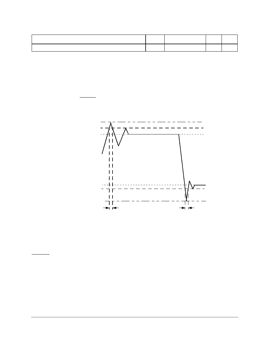
Figure 2 shows the undershoot and overshoot voltage on the MPC7441.
Figure 2. Overshoot/Undershoot Voltage
The MPC7441 provides several I/O voltages to support both compatibility with existing systems and
migration to future systems. The MPC7441 core voltage must always be provided at nominal 1.5 V (see
Table 4 for actual recommended core voltage). Voltage to the processor interface I/Os are provided through
separate sets of supply pins and may be provided at the voltages shown in Table 3. The input voltage
threshold for each bus is selected by sampling the state of the voltage select pins at the negation of the signal
HRESET. The output voltage will swing from GND to the maximum voltage applied to the OV
DD
power
pins.
Storage temperature range
T
stg
≠55 to 150
∞C
Notes:
1.
Functional and tested operating conditions are given in Table 4. Absolute maximum ratings are stress ratings
only, and functional operation at the maximums is not guaranteed. Stresses beyond those listed may affect
device reliability or cause permanent damage to the device.
2.
Caution: Vin must not exceed OV
DD
by more than 0.3 V at any time including during power-on reset.
3.
Caution: OV
DD
must not exceed V
DD
/AV
DD
by more than 2.0 V at any time including during power-on reset.
4.
Caution: V
DD
/AV
DD
must not exceed OV
DD
by more than 0.4 V at any time including during power-on reset.
5.
V
in
may overshoot/undershoot to a voltage and for a maximum duration as shown in Figure 2.
6.
BVSEL must be set to 0, such that the bus is in 1.8 V mode.
7.
BVSEL must be set to HRESET or 1, such that the bus is in 2.5 V mode.
Table 2. Absolute Maximum Ratings
1
(continued)
Characteristic
Symbol
Maximum Value
Unit
Notes
V
IH
GND
GND ≠ 0.3 V
GND ≠ 0.7 V
Not to Exceed 10%
OV
DD
+ 20%
V
IL
OV
DD
OV
DD
+ 5%
of t
SYSCLK

MOTOROLA
MPC7441 RISC Microprocessor Hardware Specifications
11
PRELIMINARY--SUBJECT TO CHANGE WITHOUT NOTICE
Electrical and Thermal Characteristics
Table 4 provides the recommended operating conditions for the MPC7441.
Table 5 provides the package thermal characteristics for the MPC7441.
Table 3. Input Threshold Voltage Setting
BVSEL Signal
Processor Bus Input Threshold is Relative to:
Notes
0
1.8 V
1, 4
¨HRESET
Not Available
1, 3
HRESET
2.5 V
1, 2
1
2.5 V
1
Notes:
1. Caution: The input threshold selection must agree with the OV
DD
/GV
DD
voltages supplied. See notes in Table 2.
2. To select the 2.5-V threshold option for the processor bus, BVSEL should be tied to HRESET so that the two
signals change state together. This is the preferred method for selecting this mode of operation.
3. ¨HRESET is the inverse of HRESET.
4. If used, pulldown resistors should be less than 250
.
Table 4. Recommended
1
Operating Conditions
Characteristic
Symbol
Recommended Value
Unit
Notes
Min
Max
Core supply voltage
V
DD
1.5 V ± 50 mV
V
PLL supply voltage
AV
DD
1.5 V ± 50 mV
V
2
Processor bus supply voltage
BVSEL = 0
OV
DD
1.8 V ± 5%
V
BVSEL = HRESET or OV
DD
OV
DD
2.5 V ± 5%
V
Input voltage
Processor bus
V
in
GND
OV
DD
V
JTAG signals
V
in
GND
OV
DD
V
Die-junction temperature
T
j
0
105
∞C
Notes:
1. These are the recommended and tested operating conditions. Proper device operation outside of these conditions
is not guaranteed.
2. This voltage is the input to the filter discussed in Section 1.9.2, "PLL Power Supply Filtering" and not necessarily
the voltage at the AV
DD
pin which may be reduced from V
DD
by the filter.
Table 5. Package Thermal Characteristics
Characteristic
Symbol
Value
Rating
CBGA package thermal resistance, junction-to-case thermal resistance
(typical)
JC
<0.1
∞C/W
CBGA package thermal resistance, die junction-to-lead thermal resistance
(typical)
JB
2.2
∞C/W
Note: Refer to Section 1.9, "System Design Information," for more details about thermal management.

12
MPC7441 RISC Microprocessor Hardware Specifications
MOTOROLA
PRELIMINARY--SUBJECT TO CHANGE WITHOUT NOTICE
Electrical and Thermal Characteristics
Table 6 provides the DC electrical characteristics for the MPC7441.
Table 7 provides the power consumption for the MPC7441.
Table 6. DC Electrical Specifications
At recommended operating conditions. See Table 4.
Characteristic
Nominal
Bus
Voltage
1
Symbol
Min
Max
Unit
Notes
Input high voltage
(all inputs except SYSCLK)
1.8
V
IH
OV
DD
◊
0.65
OV
DD
+ 0.3
V
2.5
V
IH
1.7
OV
DD
+ 0.3
V
Input low voltage
(all inputs except SYSCLK)
1.8
V
IL
≠0.3
OV
DD
◊
0.35
V
2.5
V
IL
≠0.3
0.7
V
SYSCLK input high voltage
--
CV
IH
1.4
OV
DD
+ 0.3
V
SYSCLK input low voltage
--
CV
IL
≠0.3
0.4
V
Input leakage current,
V
in
= OV
DD
+ 0.3 V
--
I
in
--
10
µA
2, 3
High impedance (off-state) leakage
current, V
in
= OV
DD
+ 0.3 V
--
I
TSI
--
10
µA
2, 3, 5
Output high voltage, I
OH
= ≠5 mA
1.8
V
OH
OV
DD
≠ 0.45
--
V
2.5
V
OH
1.7
--
V
Output low voltage, I
OL
= 5 mA
1.8
V
OL
--
0.45
V
2.5
V
OL
--
0.7
V
Capacitance,
V
in
= 0 V,
f = 1 MHz
All inputs
--
C
in
--
8.0
pF
4
Notes:
1. Nominal voltages; see Table 4 for recommended operating conditions.
2. For processor bus signals, the reference is OV
DD
.
3. Excludes test signals and IEEE 1149.1 boundary scan (JTAG) signals.
4. Capacitance is periodically sampled rather than 100% tested.
5. The leakage is measured for nominal OV
DD
and V
DD
, or both OV
DD
and V
DD
must vary in the same direction (for
example, both OV
DD
and V
DD
vary by either +5% or ≠5%).
Table 7. Power Consumption for MPC7441
Processor (CPU) Frequency
Unit
Notes
600 MHz
700 MHz
Full-Power Mode
Typical
11.5
13.4
W
1, 3
Maximum
15.4
17.6
W
1, 2
Doze Mode
Typical
--
--
W
1, 3, 4
MOTOROLA
MPC7441 RISC Microprocessor Hardware Specifications
13
PRELIMINARY--SUBJECT TO CHANGE WITHOUT NOTICE
Electrical and Thermal Characteristics
1.5.2
AC Electrical Characteristics
This section provides the AC electrical characteristics for the MPC7441. After fabrication, functional parts
are sorted by maximum processor core frequency as shown in Section 1.5.2.1, "Clock AC Specifications,"
and tested for conformance to the AC specifications for that frequency. The processor core frequency is
determined by the bus (SYSCLK) frequency and the settings of the PLL_EXT and PLL_CFG[0:3] signals.
Parts are sold by maximum processor core frequency; see Section 1.11, "Ordering Information."
1.5.2.1
Clock AC Specifications
Table 8 provides the clock AC timing specifications as defined in Figure 3.
Nap Mode
Typical
1.3
1.6
W
1, 3
Sleep Mode
Typical
0.7
0.8
W
1, 3
Deep Sleep Mode (PLL Disabled)
Typical
410
480
mW
1, 3
Notes:
1. These values apply for all valid processor bus ratios. The values do not include I/O supply power (OV
DD
) or PLL
supply power (AV
DD
). OV
DD
power is system dependent, but is typically <20% of V
DD
power. Worst case power
consumption for AV
DD
< 3 mW.
2. Maximum power is measured at nominal V
DD
(see Table 4) while running an entirely cache-resident, contrived
sequence of instructions which keep the execution units, with or without AltiVec, maximally busy.
3. Typical power is an average value measured at the nominal recommended V
DD
(see Table 4) in a system while
running a typical code sequence.
4. Doze mode is not a user-definable state; it is an intermediate state between full-power and either nap or sleep
mode. As a result, power consumption for this mode is not tested.
Table 8. Clock AC Timing Specifications
At recommended operating conditions. See Table 4.
Characteristic
Symbol
Maximum Processor Core
Frequency
Unit
Notes
600 MHz
700 MHz
Min
Max
Min
Max
Processor frequency
f
core
500
600
500
700
MHz
1
VCO frequency
f
VCO
1000
1200
1000
1400
MHz
1
SYSCLK frequency
f
SYSCLK
33
133
33
133
MHz
1
SYSCLK cycle time
t
SYSCLK
7.5
30
7.5
30
ns
SYSCLK rise and fall time
t
KR
and t
KF
--
1.0
--
1.0
ns
2
Table 7. Power Consumption for MPC7441 (continued)
Processor (CPU) Frequency
Unit
Notes
600 MHz
700 MHz
14
MPC7441 RISC Microprocessor Hardware Specifications
MOTOROLA
PRELIMINARY--SUBJECT TO CHANGE WITHOUT NOTICE
Electrical and Thermal Characteristics
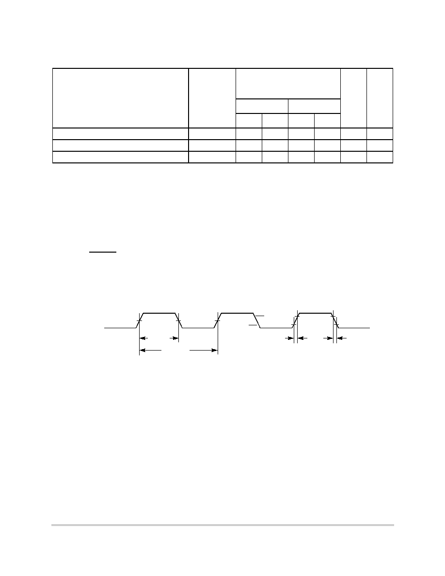
Figure 3 provides the SYSCLK input timing diagram.
Figure 3. SYSCLK Input Timing Diagram
SYSCLK duty cycle measured at OV
DD
/2
t
KHKL
/t
SYSCLK
40
60
40
60
%
3
SYSCLK jitter
--
±150
--
±150
ps
4, 6
Internal PLL relock time
--
100
--
100
µ
s
5
Notes:
1. Caution: The SYSCLK frequency, PLL_EXT and PLL_CFG[0:3] settings must be chosen such that the resulting
SYSCLK (bus) frequency, CPU (core) frequency, and PLL (VCO) frequency do not exceed their respective
maximum or minimum operating frequencies. Refer to the PLL_EXT, PLL_CFG[0:3] signal description in
Section 1.9.1, "PLL Configuration," for valid PLL_EXT and PLL_CFG[0:3] settings.
2. Rise and fall times for the SYSCLK input measured from 0.4 V to 1.4 V.
3. Timing is guaranteed by design and characterization.
4. This represents total input jitter--short term and long term combined--and is guaranteed by design.
5. Relock timing is guaranteed by design and characterization. PLL-relock time is the maximum amount of time
required for PLL lock after a stable V
DD
and SYSCLK are reached during the power-on reset sequence. This
specification also applies when the PLL has been disabled and subsequently re-enabled during sleep mode. Also
note that HRESET must be held asserted for a minimum of 255 bus clocks after the PLL-relock time during the
power-on reset sequence.
6. The SYSCLK driver's closed loop jitter bandwidth should be <500 kHz at ≠20 dB. The bandwidth must be set low
to allow cascade connected PLL-based devices to track SYSCLK drivers with the specified jitter.
Table 8. Clock AC Timing Specifications (continued)
At recommended operating conditions. See Table 4.
Characteristic
Symbol
Maximum Processor Core
Frequency
Unit
Notes
600 MHz
700 MHz
Min
Max
Min
Max
SYSCLK
VM
VM
VM
CV
IH
CV
IL
VM = Midpoint Voltage (OV
DD
/2)
t
SYSCLK
t
KR
t
KF
t
KHKL

MOTOROLA
MPC7441 RISC Microprocessor Hardware Specifications
15
PRELIMINARY--SUBJECT TO CHANGE WITHOUT NOTICE
Electrical and Thermal Characteristics
1.5.2.2
Processor Bus AC Specifications
Table 9 provides the processor bus AC timing specifications for the MPC7441 as defined in Figure 4 and
Figure 5.
Table 9. Processor Bus AC Timing Specifications
At recommended operating conditions. See Table 4.
Parameter
Symbol
2
All Speed Grades
Unit
Notes
Min
Max
Mode select input setup to HRESET
t
MVRH
8
--
t
sysclk
3, 4, 5, 6
HRESET to mode select input hold
t
MXRH
0
--
ns
3, 5
Input setup times:
A[0:35], AP[0:4], GBL, TBST, TSIZ[0:2], WT, CI,
D[0:63], DP[0:7]
AACK, ARTRY, BG, CKSTP_IN, DBG, DTI[0:3],
HRESET, INT, MCP, QACK, SMI, SRESET, TA,
TBEN, TEA, TS, EXT_QUAL, PMON_IN, SHD[0:1]
t
AVKH
t
IVKH
2.0
2.0
--
--
ns
Input hold times:
A[0:35], AP[0:4], GBL, TBST, TSIZ[0:2], WT, CI,
D[0:63], DP[0:7]
AACK, ARTRY, BG, CKSTP_IN, DBG, DTI[0:3],
HRESET, INT, MCP, QACK, SMI, SRESET, TA,
TBEN, TEA, TS, EXT_QUAL, PMON_IN, SHD[0:1]
t
AXKH
t
IXKH
0
0
--
--
ns
Output valid times:
A[0:35], AP[0:4], GBL, TBST, TSIZ[0:2], WT, CI
TS
D[0:63], DP[0:7]
ARTRY/SHD0/SHD1
BR, CKSTP_OUT, DRDY, HIT, PMON_OUT, QREQ]
t
KHAV
t
KHTSV
t
KHDV
t
KHARV
t
KHOV
--
--
--
--
--
2.5
2.5
2.5
2.5
2.5
ns
Output hold times:
A[0:35], AP[0:4], GBL, TBST, TSIZ[0:2], WT, CI
TS
D[0:63], DP[0:7]
ARTRY/SHD0/SHD1
BR, CKSTP_OUT, DRDY, HIT, PMON_OUT, QREQ
t
KHAX
t
KHTSX
t
KHDX
t
KHARX
t
KHOX
0.5
0.5
0.5
0.5
0.5
--
--
--
--
--
ns
SYSCLK to output enable
t
KHOE
0.5
--
ns
SYSCLK to output high impedance (all except TS, ARTRY,
SHD0, SHD1)
t
KHOZ
--
3.5
ns
SYSCLK to TS high impedance after precharge
t
KHTSPZ
--
1
t
sysclk
5, 7, 10
Maximum delay to ARTRY/SHD0/SHD1 precharge
t
KHARP
--
1
t
sysclk
5, 8,
9, 10

16
MPC7441 RISC Microprocessor Hardware Specifications
MOTOROLA
PRELIMINARY--SUBJECT TO CHANGE WITHOUT NOTICE
Electrical and Thermal Characteristics
Figure 4 provides the AC test load for the MPC7441.
Figure 4. AC Test Load
SYSCLK to ARTRY/SHD0/SHD1 high impedance after
precharge
t
KHARPZ
--
2
t
sysclk
5, 8,
9, 10
Notes:
1.
All input specifications are measured from the midpoint of the signal in question to the midpoint of the rising edge
of the input SYSCLK. All output specifications are measured from the midpoint of the rising edge of SYSCLK to
the midpoint of the signal in question. All output timings assume a purely resistive 50-
load (see Figure 4). Input
and output timings are measured at the pin; time-of-flight delays must be added for trace lengths, vias, and
connectors in the system.
2.
The symbology used for timing specifications herein follows the pattern of t
(signal)(state)(reference)(state)
for inputs
and t
(reference)(state)(signal)(state)
for outputs. For example, t
IVKH
symbolizes the time input signals (I) reach the valid
state (V) relative to the SYSCLK reference (K) going to the high (H) state or input setup time. And t
KHOV
symbolizes the time from SYSCLK(K) going high (H) until outputs (O) are valid (V) or output valid time. Input hold
time can be read as the time that the input signal (I) went invalid (X) with respect to the rising clock edge (KH)
(note the position of the reference and its state for inputs) and output hold time can be read as the time from the
rising edge (KH) until the output went invalid (OX).
3.
The setup and hold time is with respect to the rising edge of HRESET (see Figure 5).
4.
This specification is for configuration mode select only.
5.
t
sysclk
is the period of the external clock (SYSCLK) in nanoseconds (ns). The numbers given in the table must be
multiplied by the period of SYSCLK to compute the actual time duration (in ns) of the parameter in question.
6.
Mode select signals are: BVSEL, PLL_CFG[0:3], PLL_EXT, BMODE[0:1].
7.
According to the bus protocol, TS is driven only by the currently active bus master. It is asserted low then
precharged high before returning to high impedance as shown in Figure 6. The nominal precharge width for TS is
0.5
◊
t
SYSCLK
, i.e., less than the minimum t
SYSCLK
period, to ensure that another master asserting TS on the
following clock will not contend with the precharge. Output valid and output hold timing is tested for the signal
asserted. Output valid time is tested for precharge.The high impedance behavior is guaranteed by design.
8.
According to the bus protocol, ARTRY can be driven by multiple bus masters through the clock period
immediately following AACK. Bus contention is not an issue because any master asserting ARTRY will be driving
it low. Any master asserting it low in the first clock following AACK will then go to high impedance for one clock
before precharging it high during the second cycle after the assertion of AACK. The nominal precharge width for
ARTRY is 1.0 t
sysclk
; that is, it should be high impedance as shown in Figure 6 before the first opportunity for
another master to assert ARTRY. Output valid and output hold timing is tested for the signal asserted.The
high-impedance behavior is guaranteed by design.
9.
According to the MPX bus protocol, SHD0 and SHD1 can be driven by multiple bus masters beginning the cycle
of TS. Timing is the same as ARTRY, i.e., the signal is high impedance for a fraction of a cycle, then negated for
up to an entire cycle (crossing a bus cycle boundary) before being three-stated again. The nominal precharge
width for SHD0 and SHD1 is 1.0 t
sysclk
. The edges of the precharge vary depending on the programmed ratio of
core to bus (PLL configurations).
10. Guaranteed by design and not tested.
Table 9. Processor Bus AC Timing Specifications (continued)
At recommended operating conditions. See Table 4.
Parameter
Symbol
2
All Speed Grades
Unit
Notes
Min
Max
Output
Z
0
= 50
OV
DD
/2
R
L
= 50
MOTOROLA
MPC7441 RISC Microprocessor Hardware Specifications
17
PRELIMINARY--SUBJECT TO CHANGE WITHOUT NOTICE
Electrical and Thermal Characteristics
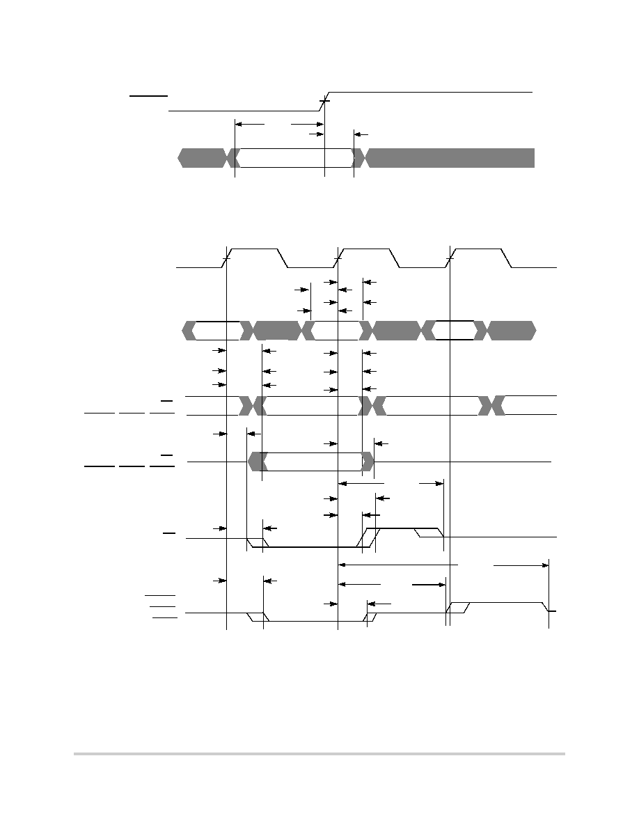
Figure 5 provides the mode select input timing diagram for the MPC7441.
Figure 5. Mode Input Timing Diagram
Figure 6 provides the input/output timing diagram for the MPC7441.
Figure 6. Input/Output Timing Diagram
HRESET
Mode Signals
t
MVRH
t
MXRH
VM = Midpoint Voltage (OV
DD
/2)
VM
SYSCLK
All Inputs
VM
VM = Midpoint Voltage (OV
DD
/2)
All Outputs
t
KHOX
VM
t
KHDV
(Except TS,
ARTRY
,
SHD0, SHD1)
All Outputs
TS
ARTRY,
(Except TS,
ARTRY
,
SHD0, SHD1)
VM
t
KHOE
t
KHOZ
t
KHTSPZ
t
KHARPZ
t
KHARP
SHD1
SHD0,
t
KHOV
t
KHAV
t
KHDX
t
KHAX
t
IXKH
t
AXKH
t
KHTSX
t
KHTSV
t
KHTSV
t
KHARV
t
KHARX
t
IVKH
t
AVKH
18
MPC7441 RISC Microprocessor Hardware Specifications
MOTOROLA
PRELIMINARY--SUBJECT TO CHANGE WITHOUT NOTICE
Electrical and Thermal Characteristics
1.5.2.3
IEEE 1149.1 AC Timing Specifications
Table 10 provides the IEEE 1149.1 (JTAG) AC timing specifications as defined in Figure 8, Figure 9,
Figure 10, and Figure 11.
Figure 7
provides the AC test load for TDO and the boundary-scan outputs of the MPC7441.
Figure 7. Alternate AC Test Load for the JTAG Interface
Table 10. JTAG AC Timing Specifications (Independent of SYSCLK)
1
At recommended operating conditions. See Table 4.
Parameter
Symbol
Min
Max
Unit
Notes
TCK frequency of operation
f
TCLK
0
33.3
MHz
TCK cycle time
t
TCLK
30
--
ns
TCK clock pulse width measured at 1.4 V
t
JHJL
15
--
ns
TCK rise and fall times
t
JR
and t
JF
0
2
ns
TRST assert time
t
TRST
25
--
ns
2
Input setup times:
Boundary-scan data
TMS, TDI
t
DVJH
t
IVJH
4
0
--
--
ns
3
Input hold times:
Boundary-scan data
TMS, TDI
t
DXJH
t
IXJH
20
25
--
--
ns
3
Valid times:
Boundary-scan data
TDO
t
JLDV
t
JLOV
4
4
20
25
ns
4
Output hold times:
Boundary-scan data
TDO
t
JLDX
t
JLOX
TBD
TBD
TBD
TBD
ns
4
TCK to output high impedance:
Boundary-scan data
TDO
t
JLDZ
t
JLOZ
3
3
19
9
ns
4, 5
5
Notes:
1. All outputs are measured from the midpoint voltage of the falling/rising edge of TCLK to the midpoint of the signal
in question. The output timings are measured at the pins. All output timings assume a purely resistive 50-
load
(see Figure 7). Time-of-flight delays must be added for trace lengths, vias, and connectors in the system.
2. TRST is an asynchronous level sensitive signal. The setup time is for test purposes only.
3. Non-JTAG signal input timing with respect to TCK.
4. Non-JTAG signal output timing with respect to TCK.
5. Guaranteed by design and characterization.
Output
Z
0
= 50
OV
DD
/2
R
L
= 50

MOTOROLA
MPC7441 RISC Microprocessor Hardware Specifications
19
PRELIMINARY--SUBJECT TO CHANGE WITHOUT NOTICE
Electrical and Thermal Characteristics
Figure 8 provides the JTAG clock input timing diagram.
Figure 8. JTAG Clock Input Timing Diagram
Figure 9 provides the TRST timing diagram.
Figure 9. TRST Timing Diagram
Figure 10 provides the boundary-scan timing diagram.
Figure 10. Boundary-Scan Timing Diagram
TCLK
VM
VM
VM
VM = Midpoint Voltage (OV
DD
/2)
t
TCLK
t
JR
t
JF
t
JHJL
TRST
t
TRST
VM = Midpoint Voltage (OV
DD
/2)
VM
VM
VM
TCK
Boundary
Boundary
Boundary
Data Outputs
Data Inputs
Data Outputs
VM = Midpoint Voltage (OV
DD
/2)
t
DXJH
t
DVJH
t
JLDV
t
JLDZ
Input
Data Valid
Output Data Valid
Output Data Valid
t
JLDX
VM
20
MPC7441 RISC Microprocessor Hardware Specifications
MOTOROLA
PRELIMINARY--SUBJECT TO CHANGE WITHOUT NOTICE
Electrical and Thermal Characteristics
Figure 11 provides the test access port timing diagram.
Figure 11. Test Access Port Timing Diagram
VM
TCK
TDI, TMS
TDO
Output Data Valid
VM
= Midpoint Voltage (OV
DD
/2)
t
IXJH
t
IVJH
t
JLOV
t
JLOZ
Input
Data Valid
TDO
Output Data Valid
t
JLOX
VM

MOTOROLA
MPC7441 RISC Microprocessor Hardware Specifications
21
PRELIMINARY--SUBJECT TO CHANGE WITHOUT NOTICE
Pin Assignments
1.6
Pin Assignments
Figure 12 (in Part A) shows the pinout of the MPC7441, 360 CBGA package as viewed from the top surface.
Part B shows the side profile of the CBGA package to indicate the direction of the top surface view.
Part A
Figure 12. Pinout of the MPC7441, 360 CBGA Package as Viewed from the Top Surface
A
B
C
D
E
F
G
H
J
K
L
M
N
P
R
T
1
2
3
4
5
6
7
8
9
10 11 12 13 14 15 16
Not to Scale
17 18 19
U
V
W
View
Part B
Die
Substrate Assembly
Encapsulant

22
MPC7441 RISC Microprocessor Hardware Specifications
MOTOROLA
PRELIMINARY--SUBJECT TO CHANGE WITHOUT NOTICE
Pinout Listings for the 360 CBGA Package
1.7
Pinout Listings for the 360 CBGA Package
Table 11 provides the pinout listing for the MPC7441, 360 CBGA package.
NOTE
This pinout is not compatible with the MPC750, MPC755, MPC7400,
or MPC7410 360 BGA package.
Table 11. Pinout Listing for the MPC7441, 360 CBGA Package
Signal Name
Pin Number
Active
I/O
I/F Select
1
Notes
A[0:35]
E11, H1, C11, G3, F10, L2, D11, D1, C10,
G2, D12, L3, G4, T2, F4, V1, J4, R2, K5,
W2, J2, K4, N4, J3, M5, P5, N3, T1, V2,
U1, N5, W1, B12, C4, G10, B11
High
I/O
BVSEL
11
AACK
R1
Low
Input
BVSEL
AP[0:4]
C1, E3, H6, F5, G7
High
I/O
BVSEL
ARTRY
N2
Low
I/O
BVSEL
8
AV
DD
A8
--
Input
N/A
BG
M1
Low
Input
BVSEL
BMODE0
G9
Low
Input
BVSEL
5
BMODE1
F8
Low
Input
BVSEL
6
BR
D2
Low
Output
BVSEL
BVSEL
B7
High
Input
BVSEL
1, 7
CI
J1
Low
Output
BVSEL
8
CKSTP_IN
A3
Low
Input
BVSEL
CKSTP_OUT
B1
Low
Output
BVSEL
CLK_OUT
H2
High
Output
BVSEL
D[0:63]
R15, W15, T14, V16, W16, T15, U15, P14,
V13, W13, T13, P13, U14, W14, R12, T12,
W12, V12, N11, N10, R11, U11, W11, T11,
R10, N9, P10, U10, R9, W10, U9, V9, W5,
U6, T5, U5, W7, R6, P7, V6, P17, R19,
V18, R18, V19, T19, U19, W19, U18, W17,
W18, T16, T18, T17, W3, V17, U4, U8, U7,
R7, P6, R8, W8, T8
High
I/O
BVSEL
DBG
M2
Low
Input
BVSEL
DP[0:7]
T3, W4, T4, W9, M6, V3, N8, W6
High
I/O
BVSEL
DRDY
R3
Low
Output
BVSEL
4
DTI[0:3]
G1, K1, P1, N1
High
Input
BVSEL
4, 13
EXT_QUAL
A11
High
Input
BVSEL
9
GBL
E2
Low
I/O
BVSEL
MOTOROLA
MPC7441 RISC Microprocessor Hardware Specifications
23
PRELIMINARY--SUBJECT TO CHANGE WITHOUT NOTICE
Pinout Listings for the 360 CBGA Package
GND
B5, C3, D6, D13, E17, F3, G17, H4, H7,
H9, H11, H13, J6, J8, J10, J12, K7, K3, K9,
K11, K13, L6, L8, L10, L12, M4, M7, M9,
M11, M13, N7, P3, P9, P12, R5, R14, R17,
T7, T10, U3, U13, U17, V5, V8, V11, V15
--
--
N/A
HIT
B2
Low
Output
BVSEL
4
HRESET
D8
Low
Input
BVSEL
INT
D4
Low
Input
BVSEL
L1_TSTCLK G8
High
Input
BVSEL
9
L2_TSTCLK
B3
High
Input
BVSEL
12
No Connect
A6, A13, A14, A15, A16, A17, A18, A19,
B13, B14, B15, B16, B17, B18, B19, C13,
C14, C15, C16, C17, C18, C19, D14, D15,
D16, D17, D18, D19, E12, E13, E14, E15,
E16, E19, F12, F13, F14, F15, F16, F17,
F18, F19, G11, G12, G13, G14, G15, G16,
G19, H14, H15, H16, H17, H18, H19, J14,
J15, J16, J17, J18, J19, K15, K16, K17,
K18, K19, L14, L15, L16, L17, L18, L19,
M14, M15, M16, M17, M18, M19, N12,
N13, N14, N15, N16, N17, N18, N19, P15,
P16, P18, P19
--
--
--
3
LSSD_MODE
E8
Low
Input
BVSEL
2, 7
MCP
C9
Low
Input
BVSEL
OV
DD
B4, C2, C12, D5, E18, F2, G18, H3, J5,
K2, L5, M3, N6, P2, P8, P11, R4, R13,
R16, T6, T9, U2, U12, U16, V4, V7, V10,
V14
--
--
N/A
PLL_CFG[0:3]
B8, C8, C7, D7
High
Input
BVSEL
PLL_EXT
A7
High
Input
BVSEL
PMON_IN
D9
Low
Input
BVSEL
10
PMON_OUT
A9
Low
Output
BVSEL
QACK
G5
Low
Input
BVSEL
QREQ
P4
Low
Output
BVSEL
SHD[0:1]
E4, H5
Low
I/O
BVSEL
8
SMI
F9
Low
Input
BVSEL
SRESET
A2
Low
Input
BVSEL
SYSCLK
A10
--
Input
BVSEL
TA
K6
Low
Input
BVSEL
TBEN
E1
High
Input
BVSEL
TBST
F11
Low
Output
BVSEL
TCK
C6
High
Input
BVSEL
Table 11. Pinout Listing for the MPC7441, 360 CBGA Package (continued)
Signal Name
Pin Number
Active
I/O
I/F Select
1
Notes

24
MPC7441 RISC Microprocessor Hardware Specifications
MOTOROLA
PRELIMINARY--SUBJECT TO CHANGE WITHOUT NOTICE
Pinout Listings for the 360 CBGA Package
TDI
B9
High
Input
BVSEL
7
TDO
A4
High
Output
BVSEL
TEA
L1
Low
Input
BVSEL
TEST[0:3]
A12, B6, B10, E10
--
Input
BVSEL
2
TEST[4]
D10
--
Input
BVSEL
9
TMS
F1
High
Input
BVSEL
7
TRST
A5
Low
Input
BVSEL
7, 14
TS
L4
Low
I/O
BVSEL
8
TSIZ[0:2]
G6, F7, E7
High
Output
BVSEL
TT[0:4]
E5, E6, F6, E9, C5
High
I/O
BVSEL
WT
D3
Low
Output
BVSEL
8
V
DD
H8, H10, H12, J7, J9, J11, J13, K8, K10,
K12, K14, L7, L9, L11, L13, M8, M10, M12
--
--
N/A
Notes:
1.
OV
DD
supplies power to the processor bus, JTAG, and all control signals; and V
DD
supplies power to the
processor core and the PLL (after filtering to become AV
DD
). To program the I/O voltage, connect BVSEL to either
GND (selects 1.8 V) or to HRESET (selects 2.5 V). If used, the pulldown resistor should be less than 250
. For
actual recommended value of V
in
or supply voltages see Table 4.
2.
These input signals are for factory use only and must be pulled up to OV
DD
for normal machine operation.
3.
These signals are for factory use only and must be left unconnected for normal machine operation.
4.
Ignored in 60x bus mode.
5.
This signal selects between MPX bus mode (asserted) and 60x bus mode (negated) and will be sampled at
HRESET going high.
6.
This signal must be negated during reset, by pull-up to OV
DD
or negation by ¨HRESET (inverse of HRESET), to
ensure proper operation.
7.
Internal pull-up on die.
8.
These pins require weak pull-up resistors (for example, 4.7 k
) to maintain the control signals in the negated
state after they have been actively negated and released by the MPC7441 and other bus masters.
9.
These input signals are for factory use only and must be pulled down to GND for normal machine operation.
10. This pin can externally enable the performance monitor counters (PMC) if they are internally enabled by the
software. If it will not be used to control the PMC, it should be pulled down to GND so that the software can
enable the PMC.
11. Unused address pins must be pulled down to GND.
12. This test signal is recommended to be tied to HRESET; however, other configurations will not adversely affect
performance.
13. These signals must be pulled down to GND if unused, or if the MPC7441 is in 60x bus mode.
14. This signal must be asserted during reset, by pull-down to GND or assertion by HRESET, to ensure proper
operation.
Table 11. Pinout Listing for the MPC7441, 360 CBGA Package (continued)
Signal Name
Pin Number
Active
I/O
I/F Select
1
Notes

MOTOROLA
MPC7441 RISC Microprocessor Hardware Specifications
25
PRELIMINARY--SUBJECT TO CHANGE WITHOUT NOTICE
Package Description
1.8
Package Description
The following sections provide the package parameters and mechanical dimensions for the CBGA package.
1.8.1
Package Parameters for the MPC7441, 360 CBGA
The package parameters are as provided in the following list. The package type is 25
◊
25 mm, 360-lead
ceramic ball grid array (CBGA).
Package outline
25
◊
25 mm
Interconnects
360 (19
◊
19 ball array ≠ 1)
Pitch
1.27 mm (50 mil)
Minimum module height
2.72 mm
Maximum module height
3.24 mm
Ball diameter
0.89 mm (35 mil)
1.8.2
Mechanical Dimensions for the MPC7441, 360 CBGA
Figure 13 provides the mechanical dimensions and
bottom surface nomenclature for the MPC7441, 360
CBGA package.

26
MPC7441 RISC Microprocessor Hardware Specifications
MOTOROLA
PRELIMINARY--SUBJECT TO CHANGE WITHOUT NOTICE
Package Description
Figure 13. Mechanical Dimensions and Bottom Surface Nomenclature for the MPC7441, 360 CBGA
NOTES:
1. DIMENSIONING AND TOLERANCING PER
ASME Y14.5M, 1994.
2. DIMENSIONS IN MILLIMETERS.
3. TOP SIDE A1 CORNER INDEX IS A
METALIZED FEATURE WITH VARIOUS
SHAPES. BOTTOM SIDE A1 CORNER IS
DESIGNATED WITH A BALL MISSING
FROM THE ARRAY.
0.2
C
A
360X
D
2X
A1 CORNER
E
e
0.2
2X
C
B
1 2 3 4 5 6 7 8 9 10 11 1213141516
A
B
C
D
E
F
G
H
J
K
L
M
N
P
R
T
B
0.3
A
0.15
b
A
0.2 A
171819
U
W
V
Millimeters
DIM
MIN
MAX
A
2.72
3.24
A1
0.80
1.00
A2
1.10
1.34
A3
--
0.6
b
0.82
0.93
D
25.00 BSC
D1
--
6.15
e
1.27 BSC
E
25.00 BSC
E1
--
10.2
E2
8.28
--
Capacitor Region
1
D1
E2
E1
A
A1
A2
A3

MOTOROLA
MPC7441 RISC Microprocessor Hardware Specifications
27
PRELIMINARY--SUBJECT TO CHANGE WITHOUT NOTICE
System Design Information
1.9
System Design Information
This section provides system and thermal design recommendations for successful application of the
MPC7441.
1.9.1
PLL Configuration
The MPC7441 PLL is configured by the PLL_EXT and PLL_CFG[0:3] signals. For a given SYSCLK (bus)
frequency, the PLL configuration signals set the internal CPU and VCO frequency of operation. PLL_EXT
will normally be pulled low but can be asserted for extended modes of operation. The PLL configuration
for the MPC7441 is shown in Table 12 for a set of example frequencies. In this example, shaded cells
represent settings that, for a given SYSCLK frequency, result in core and/or VCO frequencies that do not
comply with the 600-MHz column in Table 8.
Table 12. MPC7441 Microprocessor PLL Configuration Example for 600 MHz Parts
PLL_EXT
PLL_CFG
[0:3]
Example Bus-to-Core Frequency in MHz (VCO Frequency in MHz)
Bus-to-
Core
Multiplier
Core-to-
VCO
Multiplier
Bus
33.3 MHz
Bus
50 MHz
Bus
66.6 MHz
Bus
75 MHz
Bus
83 MHz
Bus
100 MHz
Bus
133 MHz
0
0000
0.5x
2x
16
(33)
25
(50)
33
(66)
37
(75)
47
(83)
50
(100)
66
(133)
0
0100
2x
2x
66
(133)
100
(200)
133
(266)
150
(300)
166
(333)
200
(400)
266
(533)
0
0110
2.5x
2x
83
(166)
125
(250)
166
(333)
187
(375)
208
(415)
250
(500)
333
(666)
0
1000
3x
2x
100
(200)
150
(300)
200
(400)
225
(450)
250
(500)
300
(600)
400
(800)
0
1110
3.5x
2x
116
(233)
175
(350)
233
(466)
262
(525)
291
(581)
350
(700)
466
(933)
0
1010
4x
2x
133
(266)
200
(400)
266
(533)
300
(600)
333
(666)
400
(800)
533
(1066)
0
0111
4.5x
2x
150
(300)
225
(450)
300
(600)
337
(675)
374
(747)
450
(900)
600
(1200)
0
1011
5x
2x
166
(333)
250
(500)
333
(666)
375
(750)
415
(830)
500
(1000)
667
(1333)
0
1001
5.5x
2x
183
(366)
275
(550)
366
(733)
412
(825)
457
(913)
550
(1100)
733
(1466)
0
1101
6x
2x
200
(400)
300
(600)
400
(800)
450
(900)
498
(996)
600
(1200)
0
0101
6.5x
2x
216
(433)
325
(630)
433
(866)
488
(975)
540
(1080)
650
(1300)
0
0010
7x
2x
233
(466)
350
(700)
466
(933)
525
(1050)
581
(1162)
700
(1400)
0
0001
7.5x
2x
250
(500)
375
(750)
500
(1000)
563
(1125)
623
(1245)
750
(1500)
0
1100
8x
2x
266
(533)
400
(800)
533
(1066)
600
(1200)
664
(1328)

28
MPC7441 RISC Microprocessor Hardware Specifications
MOTOROLA
PRELIMINARY--SUBJECT TO CHANGE WITHOUT NOTICE
System Design Information
1.9.2
PLL Power Supply Filtering
The AV
DD
power signal is provided on the MPC7441 to provide power to the clock generation PLL. To
ensure stability of the internal clock, the power supplied to the AV
DD
input signal should be filtered of any
noise in the 500 kHz to 10 MHz resonant frequency range of the PLL. A circuit similar to the one shown in
Figure 14 using surface mount capacitors with minimum effective series inductance (ESL) is recommended.
The circuit should be placed as close as possible to the AV
DD
pin to minimize noise coupled from nearby
circuits. It is often possible to route directly from the capacitors to the AV
DD
pin, which is on the periphery
of the 360 CBGA footprint and very close to the periphery of the 483 CBGA footprint, without the
inductance of vias.
1
0111
9x
2x
300
(600)
450
(900)
600
(1200)
675
(1350)
747
(1494)
1
1010
10x
2x
333
(666)
500
(1000)
667
(1333)
750
(1500)
1
1001
11x
2x
366
(733)
550
(1100)
733
(1466)
1
1011
12x
2x
400
(800
600
(1200)
1
0101
13x
2x
433
(866)
650
(1300)
1
1100
14x
2x
466
(933)
700
(1400)
1
0001
15x
2x
500
(1000)
750
(1500)
1
1101
16x
2x
533
(1066)
0
0011
PLL off/bypass
PLL off, SYSCLK clocks core circuitry directly
0
1111
PLL off
PLL off, no core clocking occurs
Notes:
1.
PLL_CFG[0:3] settings not listed are reserved.
2.
The sample bus-to-core frequencies shown are for reference only. Some PLL configurations may select bus, core,
or VCO frequencies which are not useful, not supported, or not tested for by the MPC7441; see Section 1.5.2.1,
"Clock AC Specifications," for valid SYSCLK, core, and VCO frequencies.
3.
In PLL-bypass mode, the SYSCLK input signal clocks the internal processor directly and the PLL is disabled.
However, the bus interface unit requires a 2x clock to function. Therefore, an additional signal, EXT_QUAL, must
be driven at one-half the frequency of SYSCLK and offset in phase to meet the required input setup t
IVKH
and hold
time t
IXKH
(see Table 9). The result will be that the processor bus frequency will be one-half SYSCLK while the
internal processor is clocked at SYSCLK frequency. This mode is intended for factory use and emulator tool use
only.
Note: The AC timing specifications given in this document do not apply in PLL-bypass mode.
4.
In PLL-off mode, no clocking occurs inside the MPC7441 regardless of the SYSCLK input.
Table 12. MPC7441 Microprocessor PLL Configuration Example for 600 MHz Parts (continued)
PLL_EXT
PLL_CFG
[0:3]
Example Bus-to-Core Frequency in MHz (VCO Frequency in MHz)
Bus-to-
Core
Multiplier
Core-to-
VCO
Multiplier
Bus
33.3 MHz
Bus
50 MHz
Bus
66.6 MHz
Bus
75 MHz
Bus
83 MHz
Bus
100 MHz
Bus
133 MHz
MOTOROLA
MPC7441 RISC Microprocessor Hardware Specifications
29
PRELIMINARY--SUBJECT TO CHANGE WITHOUT NOTICE
System Design Information
Figure 14. PLL Power Supply Filter Circuit
1.9.3
Power Supply Voltage Sequencing
The notes in Table 2 contain cautions about the sequencing of the external bus voltages and core voltage of
the MPC7441 (when they are different). These cautions are necessary for the long-term reliability of the
part. If they are violated, the electrostatic discharge (ESD) protection diodes will be forward-biased and
excessive current can flow through these diodes. If the system power supply design does not control the
voltage sequencing, the circuit shown in Figure 15 can be added to meet these requirements. The 30BF10
diodes (see Figure 15) control the maximum potential difference between the external bus and core power
supplies on power-up and the 1N5820 diodes regulate the maximum potential difference on power-down.
Figure 15. Example Voltage Sequencing Circuit
1.9.4
Decoupling Recommendations
Due to the MPC7441 dynamic power management feature, large address and data buses, and high operating
frequencies, the MPC7441 can generate transient power surges and high frequency noise in its power
supply, especially while driving large capacitive loads. This noise must be prevented from reaching other
components in the MPC7441 system, and the MPC7441 itself requires a clean, tightly regulated source of
power. Therefore, it is recommended that the system designer place at least one decoupling capacitor at each
V
DD
and OV
DD
pin of the MPC7441. It is also recommended that these decoupling capacitors receive their
power from separate V
DD
, OV
DD
, and GND power planes in the PCB, utilizing short traces to minimize
inductance.
These capacitors should have a value of 0.01 µF or 0.1 µF. Only ceramic surface mount technology (SMT)
capacitors should be used to minimize lead inductance, preferably 0508 or 0603 orientations where
connections are made along the length of the part. Consistent with the recommendations of Dr. Howard
Johnson in High Speed Digital Design: A Handbook of Black Magic (Prentice Hall, 1993) and contrary to
previous recommendations for decoupling Motorola microprocessors, multiple small capacitors of equal
value are recommended over using multiple values of capacitance.
In addition, it is recommended that there be several bulk storage capacitors distributed around the PCB,
feeding the V
DD
and OV
DD
planes, to enable quick recharging of the smaller chip capacitors. These bulk
capacitors should have a low equivalent series resistance (ESR) rating to ensure the quick response time
V
DD
AV
DD
10
2.2 µF
2.2 µF
GND
Low ESL Surface Mount Capacitors
2.5 V
1.5 V
1N5820
1N5820
30BF10
30BF10

30
MPC7441 RISC Microprocessor Hardware Specifications
MOTOROLA
PRELIMINARY--SUBJECT TO CHANGE WITHOUT NOTICE
System Design Information
necessary. They should also be connected to the power and ground planes through two vias to minimize
inductance. Suggested bulk capacitors: 100≠330 µF (AVX TPS tantalum or Sanyo OSCON).
1.9.5
Connection Recommendations
To ensure reliable operation, it is highly recommended to connect unused inputs to an appropriate signal
level. Unused active low inputs should be tied to OV
DD
. Unused active high inputs should be connected to
GND. All NC (no-connect) signals must remain unconnected.
Power and ground connections must be made to all external V
DD
, OV
DD
, and GND pins in the MPC7441.
1.9.6
Output Buffer DC Impedance
The MPC7441 processor bus drivers is characterized over process, voltage, and temperature. To measure
Z
0
, an external resistor is connected from the chip pad to OV
DD
or GND. Then, the value of each resistor is
varied until the pad voltage is OV
DD
/2 (see Figure 16).
The output impedance is the average of two components, the resistances of the pull-up and pull-down
devices. When data is held low, SW2 is closed (SW1 is open), and R
N
is trimmed until the voltage at the
pad equals OV
DD
/2. R
N
then becomes the resistance of the pull-down devices. When data is held high, SW1
is closed (SW2 is open), and R
P
is trimmed until the voltage at the pad equals OV
DD
/2. R
P
then becomes
the resistance of the pull-up devices. R
P
and R
N
are designed to be close to each other in value. Then, Z
0
=
(R
P
+ R
N
)/2.
Figure 16. Driver Impedance Measurement
Table 13 summarizes the signal impedance results. The impedance increases with junction temperature and
is relatively unaffected by bus voltage.
OV
DD
OGND
R
P
R
N
Pad
Data
SW1
SW2

MOTOROLA
MPC7441 RISC Microprocessor Hardware Specifications
31
PRELIMINARY--SUBJECT TO CHANGE WITHOUT NOTICE
System Design Information
1.9.7
Pull-Up/Pull-Down Resistor Requirements
The MPC7441 requires high-resistive (weak: 4.7 k
) pull-up resistors on several control pins of the bus
interface to maintain the control signals in the negated state after they have been actively negated and
released by the MPC7441 or other bus masters. These pins are: TS, ARTRY, SHDO, and SHD1.
Some pins designated as being for factory test must be pulled up to OV
DD
or down to GND to ensure proper
device operation. For the MPC7441, 360 BGA, the pins that must be pulled up to OV
DD
are: LSSD_MODE
and TEST[0:3]; the pins that must be pulled down to GND are: L1_TSTCLK and TEST[4].
In addition, the MPC7441 has one open-drain style output that requires a pull-up resistor (weak or stronger:
4.7 k
≠1 k
) if it is used by the system. This pin is CKSTP_OUT.
If a pull-down resistor is used to configure BVSEL, the resistor should be less than 250
(see Table 11).
During inactive periods on the bus, the address and transfer attributes may not be driven by any master and
may, therefore, float in the high-impedance state for relatively long periods of time. Because the MPC7441
must continually monitor these signals for snooping, this float condition may cause excessive power draw
by the input receivers on the MPC7441 or by other receivers in the system. It is recommended that these
signals be pulled up through weak (4.7 k
) pull-up resistors by the system, or that they may be otherwise
driven by the system during inactive periods of the bus. The snooped address and transfer attribute inputs
are: A[0:35], AP[0:4], TT[0:4], CI, WT, and GBL.
If extended addressing is not used, A[0:3] are unused and must be be pulled low to GND through weak
pull-down resistors. If the MPC7441 is in 60x bus mode, DTI[0:3] must be pulled low to GND through weak
pull-down resistors.
The data bus input receivers are normally turned off when no read operation is in progress and, therefore,
do not require pull-up resistors on the bus. Other data bus receivers in the system, however, may require
pull-ups, or that those signals be otherwise driven by the system during inactive periods by the system. The
data bus signals are: D[0:63] and DP[0:7].
If address or data parity is not used by the system, and the respective parity checking is disabled through
HID0, the input receivers for those pins are disabled, and those pins do not require pull-up resistors and
should be left unconnected by the system. If all parity generation is disabled through HID0, then all parity
checking should also be disabled through HID0, and all parity pins may be left unconnected by the system.
1.9.8
JTAG Configuration Signals
Boundary scan testing is enabled through the JTAG interface signals. The TRST signal is optional in the
IEEE 1149.1 specification, but is provided on all processors that implement the PowerPC architecture.
While it is possible to force the TAP controller to the reset state using only the TCK and TMS signals, more
reliable power-on reset performance will be obtained if the TRST signal is asserted during power-on reset.
Because the JTAG interface is also used for accessing the common on-chip processor (COP) function,
simply tying TRST to HRESET is not practical.
Table 13. Impedance Characteristics
V
DD
= 1.5 V, OV
DD
= 1.8 V ± 5%, T
j
= 5∞≠85∞C
Impedance
Processor Bus
Unit
Z
0
Typical
33≠42
Maximum
31≠51

32
MPC7441 RISC Microprocessor Hardware Specifications
MOTOROLA
PRELIMINARY--SUBJECT TO CHANGE WITHOUT NOTICE
System Design Information
The COP function of these processors allows a remote computer system (typically, a PC with dedicated
hardware and debugging software) to access and control the internal operations of the processor. The COP
interface connects primarily through the JTAG port of the processor, with some additional status monitoring
signals. The COP port requires the ability to independently assert HRESET or TRST in order to fully control
the processor. If the target system has independent reset sources, such as voltage monitors, watchdog timers,
power supply failures, or push-button switches, then the COP reset signals must be merged into these signals
with logic.
The arrangement shown in Figure 17 allows the COP to independently assert HRESET or TRST, while
ensuring that the target can drive HRESET as well. An optional pull-down resistor on TRST can be
populated to ensure that the JTAG scan chain is initialized during power-on if the JTAG interface and COP
header will not be used; otherwise, this resistor should be unpopulated and TRST is asserted when the
system reset signal (HRESET) is asserted and the JTAG interface is responsible for driving TRST when
needed.
The COP header shown in Figure 17 adds many benefits--breakpoints, watchpoints, register and memory
examination/modification, and other standard debugger features are possible through this interface--and
can be as inexpensive as an unpopulated footprint for a header to be added when needed.
The COP interface has a standard header for connection to the target system, based on the 0.025"
square-post, 0.100" centered header assembly (often called a Berg header). The connector typically has
pin 14 removed as a connector key.
There is no standardized way to number the COP header shown in Figure 17; consequently, many different
pin numbers have been observed from emulator vendors. Some are numbered top-to-bottom then
left-to-right, while others use left-to-right then top-to-bottom, while still others number the pins counter
clockwise from pin 1 (as with an IC). Regardless of the numbering, the signal placement recommended in
Figure 17 is common to all known emulators.
The QACK signal shown in Figure 17 is usually connected to the PCI bridge chip in a system and is an input
to the MPC7441 informing it that it can go into the quiescent state. Under normal operation this occurs
during a low-power mode selection. In order for COP to work, the MPC7441 must see this signal asserted
(pulled down). While shown on the COP header, not all emulator products drive this signal. If the product
does not, a pull-down resistor can be populated to assert this signal. Additionally, some emulator products
implement open-drain type outputs and can only drive QACK asserted; for these tools, a pull-up resistor can
be implemented to ensure this signal is deasserted when it is not being driven by the tool. Note that the
pull-up and pull-down resistors on the QACK signal are mutually exclusive and it is never necessary to
populate both in a system. To preserve correct power down operation, QACK should be merged via logic
so that it also can be driven by the PCI bridge.
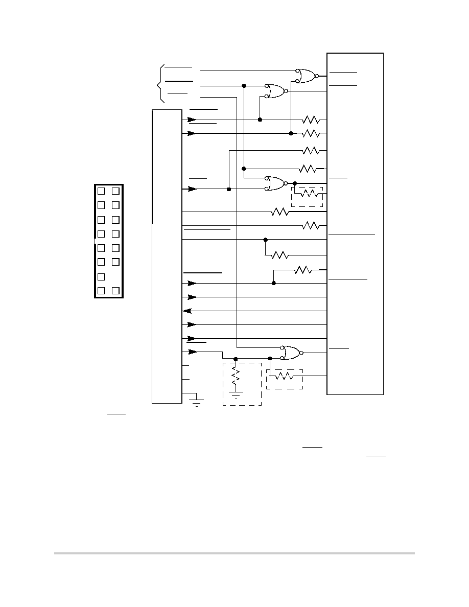
MOTOROLA
MPC7441 RISC Microprocessor Hardware Specifications
33
PRELIMINARY--SUBJECT TO CHANGE WITHOUT NOTICE
System Design Information
Figure 17. JTAG Interface Connection
1.9.9
Thermal Management Information
This section provides thermal management information for the ceramic ball grid array (CBGA) package for
air-cooled applications. Proper thermal control design is primarily dependent on the system-level
design--the heat sink, airflow, and thermal interface material. To reduce the die-junction temperature, heat
HRESET
HRESET
From Target
Board Sources
HRESET
13
SRESET
SRESET
SRESET
NC
NC
11
VDD_SENSE
6
5
1
15
2 k
10 k
10 k
10 k
OV
DD
OV
DD
OV
DD
OV
DD
CHKSTP_IN
CHKSTP_IN
8
TMS
TDO
TDI
TCK
TMS
TDO
TDI
TCK
9
1
3
4
TRST
7
16
2
10
12
(if any)
C
O
P H
ead
er
14
2
Key
Notes:
1. RUN/STOP, normally found on pin 5 of the COP header, is not implemented on the MPC7450.
Connect pin 5 of the COP header to OV
DD
with a 10 K
pull-up resistor.
2. Key location; Pin 14 is not physically present on the COP header.
.
QACK
OV
DD
OV
DD
10 k
OV
DD
2 k
3
GND
3. Component not populated. Populate only if JTAG interface is unused.
TRST
10 k
OV
DD
10 k
10 k
QACK
2 k
4
QACK
CHKSTP_OUT
CHKSTP_OUT
3
13
9
5
1
6
10
2
15
11
7
16
12
8
4
KEY
No pin
COP Connector
Physical Pin Out
4. Component not populated. Populate only if debug tool does not drive QACK.
10 k
5
OV
DD
5. Populate only if debug tool uses an open-drain type output and does not actively deassert QACK.
1
2 k
4

34
MPC7441 RISC Microprocessor Hardware Specifications
MOTOROLA
PRELIMINARY--SUBJECT TO CHANGE WITHOUT NOTICE
System Design Information
sinks may be attached to the package by several methods--spring clip to holes in the printed-circuit board
or package, and mounting clip and screw assembly (see Figure 18); however, due to the potential large mass
of the heat sink, attachment through the printed circuit board is suggested. If a spring clip is used, the spring
force should not exceed 5.5 pounds.
Figure 18. Package Exploded Cross-Sectional View with Several Heat Sink Options
The board designer can choose between several types of heat sinks to place on the MPC7441. There are
several commercially available heat sinks for the MPC7441 provided by the following vendors:
Chip Coolers Inc.
800-227-0254 (USA/Canada)
333 Strawberry Field Rd.
401-739-7600
Warwick, RI 02887-6979
Internet: www.chipcoolers.com
International Electronic Research Corporation (IERC)
818-842-7277
135 W. Magnolia Blvd.
Burbank, CA 91502
Internet: www.ctscorp.com
Thermalloy
972-243-4321
2021 W. Valley View Lane
Dallas, TX 75234-8993
Internet: www.thermalloy.com
Wakefield Engineering
781-406-3000
100 Cummings Center, Suite 157H
Beverly, MA 01915
Internet: www.wakefield.com
Aavid Engineering
972-551-7330
250 Apache Trail
Terrell, TX 75160
Internet: www.aavid.com
Thermal Interface Material
Heat Sink
CBGA Package
Heat Sink
Clip
Printed-Circuit Board

MOTOROLA
MPC7441 RISC Microprocessor Hardware Specifications
35
PRELIMINARY--SUBJECT TO CHANGE WITHOUT NOTICE
System Design Information
Cool Innovations Inc.
905-760-1992
260 Spinnaker Way, Unit 8
Concord, Ontario L4K 4P9
Canada
Internet: www.coolinnovations.com
Ultimately, the final selection of an appropriate heat sink depends on many factors, such as thermal
performance at a given air velocity, spatial volume, mass, attachment method, assembly, and cost.
1.9.9.1
Internal Package Conduction Resistance
For the exposed-die packaging technology, shown in Table 3, the intrinsic conduction thermal resistance
paths are as follows:
∑
The die junction-to-case (or top-of-die for exposed silicon) thermal resistance
∑
The die junction-to-ball thermal resistance
Figure 19 depicts the primary heat transfer path for a package with an attached heat sink mounted to a
printed-circuit board.
Figure 19. C4 Package with Heat Sink Mounted to a Printed-Circuit Board
Heat generated on the active side of the chip is conducted through the silicon, then through the heat sink
attach material (or thermal interface material), and finally to the heat sink where it is removed by forced-air
convection.
Because the silicon thermal resistance is quite small, for a first-order analysis, the temperature drop in the
silicon may be neglected. Thus, the thermal interface material and the heat sink conduction/convective
thermal resistances are the dominant terms.
1.9.9.2
Thermal Interface Materials
A thermal interface material is recommended at the package lid-to-heat sink interface to minimize the
thermal contact resistance. For those applications where the heat sink is attached by spring clip mechanism,
Figure 20 shows the thermal performance of three thin-sheet thermal-interface materials (silicone,
External Resistance
External Resistance
Internal Resistance
(Note the internal versus external package resistance)
Radiation
Convection
Radiation
Convection
Heat Sink
Printed-Circuit Board
Thermal Interface Material
Package/Leads
Die Junction
Die/Package

36
MPC7441 RISC Microprocessor Hardware Specifications
MOTOROLA
PRELIMINARY--SUBJECT TO CHANGE WITHOUT NOTICE
System Design Information
graphite/oil, floroether oil), a bare joint, and a joint with thermal grease as a function of contact pressure.
As shown, the performance of these thermal interface materials improves with increasing contact pressure.
The use of thermal grease significantly reduces the interface thermal resistance. That is, the bare joint results
in a thermal resistance approximately 7 times greater than the thermal grease joint.
Often, heat sinks are attached to the package by means of a spring clip to holes in the printed-circuit board
(see Figure 18). Therefore, the synthetic grease offers the best thermal performance, considering the low
interface pressure and is recommended due to the high power dissipation of the MPC7441. Of course, the
selection of any thermal interface material depends on many factors--thermal performance requirements,
manufacturability, service temperature, dielectric properties, cost, etc.
Figure 20. Thermal Performance of Select Thermal Interface Material
The board designer can choose between several types of thermal interface. Heat sink adhesive materials
should be selected based upon high conductivity, yet adequate mechanical strength to meet equipment
shock/vibration requirements. There are several commercially available thermal interfaces and adhesive
materials provided by the following vendors:
Dow-Corning Corporation
800-248-2481
Dow-Corning Electronic Materials
PO Box 0997
Midland, MI 48686-0997
Internet: www.dow.com
Chomerics, Inc.
781-935-4850
77 Dragon Court
Woburn, MA 01888-4014
Internet: www.chomerics.com
0
0.5
1
1.5
2
0
10
20
30
40
50
60
70
80
Silicone Sheet (0.006 inch)
Bare Joint
Floroether Oil Sheet (0.007 inch)
Graphite/Oil Sheet (0.005 inch)
Synthetic Grease
Contact Pressure (psi)
Spec
ifi
c
Ther
mal
R
e
s
i
s
t
an
ce
(Kin
2
/W
)

MOTOROLA
MPC7441 RISC Microprocessor Hardware Specifications
37
PRELIMINARY--SUBJECT TO CHANGE WITHOUT NOTICE
System Design Information
Thermagon Inc.
888-246-9050
3256 West 25th Street
Cleveland, OH 44109-1668
Internet: www.thermagon.com
Loctite Corporation
860-571-5100
1001 Trout Brook Crossing
Rocky Hill, CT 06067-3910
Internet: www.loctite.com
The following section provides a heat sink selection example using one of the commercially available heat
sinks.
1.9.9.3
Heat Sink Selection Example
For preliminary heat sink sizing, the die-junction temperature can be expressed as follows:
T
j
= T
a
+ T
r
+ (
jc
+
int
+
sa
)
◊
P
d
where:
T
j
is the die-junction temperature
T
a
is the inlet cabinet ambient temperature
T
r
is the air temperature rise within the computer cabinet
jc
is the junction-to-case thermal resistance
int
is the adhesive or interface material thermal resistance
sa
is the heat sink base-to-ambient thermal resistance
P
d
is the power dissipated by the device
During operation, the die-junction temperatures (T
j
) should be maintained less than the value specified in
Table 4. The temperature of the air cooling the component greatly depends upon the ambient inlet air
temperature and the air temperature rise within the electronic cabinet. An electronic cabinet inlet-air
temperature (T
a
) may range from 30∞ to 40∞C. The air temperature rise within a cabinet (T
r
) may be in the
range of 5∞ to 10∞C. The thermal resistance of the thermal interface material (
int
) is typically about
1.5∞C/W. For example, assuming a T
a
of 30∞C, a T
r
of 5∞C, a CBGA package
jc
= 0.1, and a typical power
consumption (P
d
) of 11.5 W, the following expression for T
j
is obtained:
Die-junction temperature:
T
j
= 30∞C + 5∞C + (0.1∞C/W + 1.5∞C/W +
sa
)
◊
11.5 W
For this example, a
sa
value of 4.4∞C/W or less is required to maintain the die junction temperature below
the maximum value of Table 4.
Though the die junction-to-ambient and the heat sink-to-ambient thermal resistances are a common
figure-of-merit used for comparing the thermal performance of various microelectronic packaging
technologies, one should exercise caution when only using this metric in determining thermal management
because no single parameter can adequately describe three-dimensional heat flow. The final die-junction
operating temperature is not only a function of the component-level thermal resistance, but the system-level
design and its operating conditions. In addition to the component's power consumption, a number of factors
affect the final operating die-junction temperature--airflow, board population (local heat flux of adjacent
components), heat sink efficiency, heat sink attach, heat sink placement, next-level interconnect technology,
system air temperature rise, altitude, etc.
Due to the complexity and the many variations of system-level boundary conditions for today's
microelectronic equipment, the combined effects of the heat transfer mechanisms (radiation, convection,

38
MPC7441 RISC Microprocessor Hardware Specifications
MOTOROLA
PRELIMINARY--SUBJECT TO CHANGE WITHOUT NOTICE
Document Revision History
and conduction) may vary widely. For these reasons, we recommend using conjugate heat transfer models
for the board, as well as system-level designs.
1.10 Document Revision History
Table 14 provides a revision history for this hardware specification.
1.11 Ordering Information
Ordering information for the parts fully covered by this specification document is provided in
Section 1.11.1, "Part Numbers Fully Addressed by This Document."
1.11.1 Part Numbers Fully Addressed by This Document
Table 15 provides the Motorola part numbering nomenclature for the MPC7441. Note that the individual
part numbers correspond to a maximum processor core frequency. For available frequencies, contact your
local Motorola sales office. In addition to the processor frequency, the part numbering scheme also includes
an application modifier which may specify special application conditions. Each part number also contains
a revision level code which refers to the die mask revision number.
Table 14. Document Revision History
Document Revision
Substantive Change(s)
Rev 0
Initial release.
Table 15. Part Numbering Nomenclature
XPC
7441
RX
nnn
x
x
Product
Code
Part
Identifier
Package
Processor
Frequency
1
Application Modifier
Revision Level
XPC
2
7441
RX = CBGA
600
700
L: 1.5 V ± 50 mV
0 to 105
∞
C
G: 2.3; PVR = 8000 0210
Notes:
1. Processor core frequencies supported by parts addressed by this specification only. Parts addressed by Part
Number Specifications may support other maximum core frequencies.
2. The X prefix in a Motorola part number designates a "Pilot Production Prototype" as defined by Motorola SOP
3-13. These are from a limited production volume of prototypes manufactured, tested, and Q.A. inspected on a
qualified technology to simulate normal production. These parts have only preliminary reliability and
characterization data. Before pilot production prototypes may be shipped, written authorization from the customer
must be on file in the applicable sales office acknowledging the qualification status and the fact that product
changes may still occur while shipping pilot production prototypes.
MOTOROLA
MPC7441 RISC Microprocessor Hardware Specifications
39
PRELIMINARY--SUBJECT TO CHANGE WITHOUT NOTICE
Ordering Information
1.11.2 Part Marking
Parts are marked as the example shown in Figure 21.
Figure 21. Part Marking for BGA Device
BGA
Notes
:
CCCCC is the country of assembly. This space is left blank if parts are assembled in the United States.
MMMMMM is the 6-digit mask number.
ATWLYYWWA is the traceability code.
XPC7441
RX600LG
MMMMMM
ATWLYYWWA
7441

MPC7441EC/D
HOW TO REACH US:
USA/EUROPE/LOCATIONS NOT LISTED:
Motorola Literature Distribution;
P.O. Box 5405, Denver, Colorado 80217
1-303-675-2140 or 1-800-441-2447
JAPAN:
Motorola Japan Ltd.; SPS, Technical Information Center,
3-20-1, Minami-Azabu Minato-ku, Tokyo 106-8573 Japan
81-3-3440-3569
ASIA/PACIFIC:
Motorola Semiconductors H.K. Ltd.; Silicon Harbour
Centre, 2 Dai King Street, Tai Po Industrial Estate,
Tai Po, N.T., Hong Kong
852-26668334
TECHNICAL INFORMATION CENTER:
1-800-521-6274
HOME PAGE:
http://www.motorola.com/semiconductors
DOCUMENT COMMENTS:
FAX (512) 933-2625,
Attn: RISC Applications Engineering
Information in this document is provided solely to enable system and software
implementers to use . There are no express or implied copyright licenses granted
hereunder to design or fabricate any integrated circuits or integrated circuits based
on the information in this document.
Motorola reserves the right to make changes without further notice to any products
herein. Motorola makes no warranty, representation or guarantee regarding the
suitability of its products for any particular purpose, nor does Motorola assume any
liability arising out of the application or use of any product or circuit, and specifically
disclaims any and all liability, including without limitation consequential or incidental
damages. "Typical" parameters which may be provided in Motorola data sheets
and/or specifications can and do vary in different applications and actual
performance may vary over time. All operating parameters, including "Typicals"
must be validated for each customer application by customer's technical experts.
Motorola does not convey any license under its patent rights nor the rights of
others. Motorola products are not designed, intended, or authorized for use as
components in systems intended for surgical implant into the body, or other
applications intended to support or sustain life, or for any other application in which
the failure of the Motorola product could create a situation where personal injury or
death may occur. Should Buyer purchase or use Motorola products for any such
unintended or unauthorized application, Buyer shall indemnify and hold Motorola
and its officers, employees, subsidiaries, affiliates, and distributors harmless
against all claims, costs, damages, and expenses, and reasonable attorney fees
arising out of, directly or indirectly, any claim of personal injury or death associated
with such unintended or unauthorized use, even if such claim alleges that Motorola
was negligent regarding the design or manufacture of the part.
Motorola and the Stylized M Logo are registered in the U.S. Patent and Trademark
Office. digital dna is a trademark of Motorola, Inc. All other product or service
names are the property of their respective owners. Motorola, Inc. is an Equal
Opportunity/Affirmative Action Employer.
© Motorola, Inc. 2001