This document describes part-number-specific changes to recommended operating conditions
and revised electrical specifications, as applicable, from those described in the general
MPC755 RISC Microprocessor Hardware Specifications (order # MPC755EC/D).
Specifications provided in this document supersede those in the MPC755 RISC
Microprocessor Hardware Specifications, Rev. 4 or later, for the part numbers listed in
Table A only. Specifications not addressed herein are unchanged. Because this document is
frequently updated, refer to http://www.motorola.com/semiconductors or to your Motorola
sales office for the latest version.
Note that headings and table numbers in this document are not consecutively numbered. They
are intended to correspond to the heading or table affected in the general hardware
specification.
Part numbers addressed in this document are listed in Table A. For more detailed ordering
information see Section 1.11.
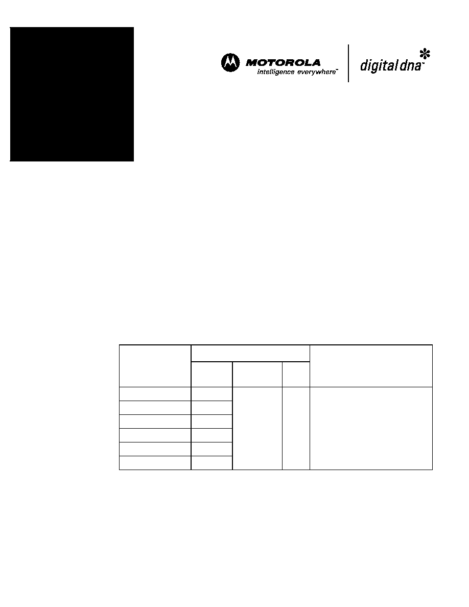
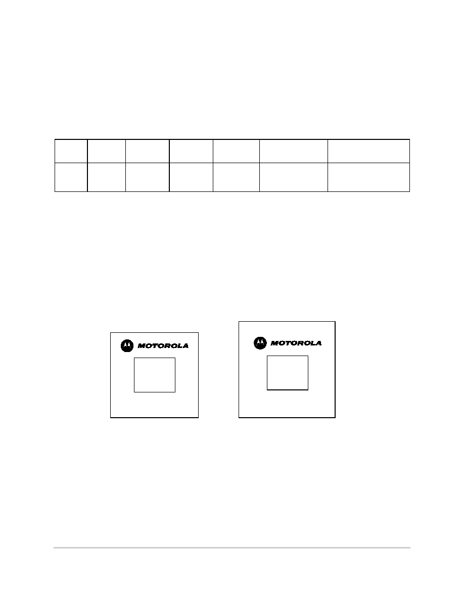
Table A. Significant Differences from Hardware Specification by
Part Number
Motorola
Part Number
Operating Conditions
Significant Differences from
Hardware Specification
CPU
Frequency
V
DD
T
J
(∞C)
XPC755BRX300LD
300 MHz
2.0 V ±100 mV 0 to 105 2.0 V/1.8 V I/O voltage supported, 2.5 V
I/O not supported; all nominal core
voltages are 2.0 V ±100 mV; AC timing
different for processor bus and L2 bus
interfaces; L2 bus interface AC timing
not guaranteed in 1.8 V/2.0 V mode.
XPC755BRX350LD
350 MHz
XPC755BRX400LD
400 MHz
XPC755BPX300LD
300 MHz
XPC755BPX350LD
350 MHz
XPC755BPX400LD
400 MHz
Advance Information
MPC755BLDPNS/D
Rev. 2, 4/2002
MPC755 Part Number
Specification for the
XPC755BxxnnnLD and
XPC745BxxnnnLD Series
Motorola Part
Numbers Affected:
XPC755BRX300LD
XPC755BRX350LD
XPC755BRX400LD
XPC755BPX300LD
XPC755BPX350LD
XPC755BPX400LD
XPC745BPX300LD
XPC745BPX350LD
2
MPC755 Part Number Specification for the
MOTOROLA
XPC755B
xxnnn
LD and XPC745B
xxnnn
LD Series
General Parameters
There are currently no known errata for the part numbers addressed by this data sheet.
1.3 General Parameters
The following general parameters apply to all part numbers described herein:
Core power supply
2.0 V ±100 mV DC (nominal; see Table 3 for recommended operating
conditions)
I/O power supply
1.8 V ±100 mV dc (processor bus interface only; not supported on
L2 interface), or
2.0 V ±100 mV dc (processor bus interface only; not supported on
L2 interface), or
3.3 V ±165 mV dc (input thresholds are configuration pin selectable)
Note that part revisions prior to Rev. 2.8 (Rev. E) do not support core voltages down to 1.8 V.
1.4.1 DC Electrical Characteristics
All part numbers affected by this specification support 3.3 V and 1.8 V/2.0 V I/O voltages, but do not
support 2.5 V I/O voltages. Table 2 describes the input threshold voltage settings. These settings apply to
all device revisions prior to Rev. 2.8 (Rev. E), including all part numbers described herein. Note that the
MPC745 does not provide an L2 interface.
XPC745BPX300LD
300 MHz
2.0 V ±100 mV 0 to 105 2.0 V/1.8 V I/O voltage supported,
2.5 V I/O not supported; all nominal
core voltages are 2.0 V ±100 mV; AC
timing different for processor bus
interface.
XPC745BPX350LD
350 MHz
Note: The X prefix in a Motorola PowerPC part number designates a "Pilot Production Prototype" as
defined by Motorola SOP 3-13. These are from a limited production volume of prototypes
manufactured, tested, and Q.A. inspected on a qualified technology to simulate normal production.
These parts have only preliminary reliability and characterization data. Before pilot production
prototypes may be shipped, written authorization from the customer must be on file in the applicable
sales office acknowledging the qualification status and the fact that product changes may still occur
while shipping pilot production prototypes.
Table A. Significant Differences from Hardware Specification by
Part Number (continued)
Motorola
Part Number
Operating Conditions
Significant Differences from
Hardware Specification
CPU
Frequency
V
DD
T
J
(∞C)
MOTOROLA
MPC755 Part Number Specification for the
3
XPC755B
xxnnn
LD and XPC745B
xxnnn
LD Series
General Parameters
Table 3 provides the recommended operating conditions for all device revisions prior to Rev. 2.8 (Rev. E),
including all part numbers described herein.
Table 6 provides the DC electrical specifications for all device revisions prior to Rev. 2.8 (Rev. E), including
all part numbers described herein.
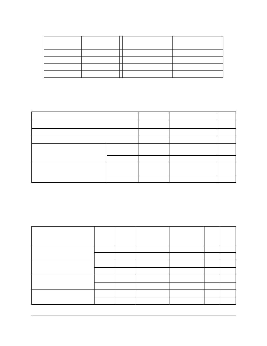
Table 2. Input Threshold Voltage Setting
BVSEL Signal
L2VSEL Signal
Processor Bus
Interface Voltage
L2 Bus
Interface Voltage
0
0
1.8 V or 2.0 V
1.8 V or 2.0 V
0
1
1.8 V or 2.0 V
3.3 V
1
0
3.3 V
1.8 V or 2.0 V
1
1
3.3 V
3.3 V
Caution: The input threshold selection must agree with the OV
DD
/L2OV
DD
voltages supplied.
Table 3. Recommended Operating Conditions
Characteristic
Symbol
Recommended Value
Unit
Core supply voltage
V
DD
2.0 ±100 mV
V
PLL supply voltage
AV
DD
2.0 ±100 mV
V
L2 DLL supply voltage
L2AV
DD
2.0 ±100 mV
V
Processor bus supply voltage
BVSEL = 0
OV
DD
1.8 ±100 mV or
2.0 ±100 mV
V
BVSEL = 1
OV
DD
3.3 ±165 mV
V
L2 bus supply voltage
L2VSEL = 0
L2OV
DD
1.8 ±100 mV or
2.0 ±100 mV
V
L2VSEL = 1
L2OV
DD
3.3 ±165 mV
V
Note: These are the recommended and tested operating conditions. Proper device operation outside of these
conditions is not guaranteed.
Table 6. DC Electrical Specifications
At recommended operating conditions (see Table 3)
Characteristic
Nominal
Bus
Voltage
1
Symbol
Min
Max
Unit
Notes
Input high voltage (all inputs except
SYSCLK)
1.8/2.0
V
IH
0.65
◊
(L2)OV
DD
(L2)OV
DD
+ 0.3
V
2,3
3.3
V
IH
2.0
(L2)OV
DD
+ 0.3
V
2,3
Input low voltage (all inputs except
SYSCLK)
1.8/2.0
V
IL
≠0.3
0.35
◊
(L2)OV
DD
V
2
3.3
V
IL
≠0.3
0.8
V
SYSCLK input high voltage
1.8/2.0
KV
IH
1.5
OV
DD
+ 0.3
V
3.3
KV
IH
2.4
OV
DD
+ 0.3
V
SYSCLK input low voltage
1.8/2.0
KV
IL
≠0.3
0.2
V
3.3
KV
IL
≠0.3
0.4
V

4
MPC755 Part Number Specification for the
MOTOROLA
XPC755B
xxnnn
LD and XPC745B
xxnnn
LD Series
General Parameters
1.4.2.2 Processor Bus AC Specifications
All part numbers described herein have slower AC timing characteristics than later revisions of the part. The
affected processor bus AC timing specifications are given in Table 10.
1.4.2.4 L2 Bus AC Specifications
The AC timing characteristics of the L2 bus interface in 3.3 V mode are slower for parts affected by this
specification than for later revisions of the part. Additionally, the AC timing of the L2 interface is not
guaranteed in 1.8 V/2.0 V mode. These affect the following part numbers only:
∑
XPC755BRX300LD
∑
XPC755BRX350LD
∑
XPC755BRX400LD
∑
XPC755BPX300LD
∑
XPC755BPX350LD
∑
XPC755BPX400LD
Table 12 provides the L2 bus interface AC timing specifications for the MPC755 described in this document
when the L2 bus interface is in 3.3 V mode only. The L2 bus interface of the part described herein is not
tested in 1.8 V/2.0 V mode and does not meet these specifications. The L2 interface output drivers may
display a non-linear, stepped behavior when switching that prolongs the rise and fall times in this mode. This
behavior is dependent on L2OV
DD
, the impedance of the circuit board, and operating conditions of the
processor. In a worst-case device, at L2OV
DD
= 1.8 V and T
j
= 105
∞
C, the driver output impedance is 55
;
at L2OV
DD
= 2.0 V and T
j
= 105
∞
C, the driver output impedance is 47
. The non-linear behavior results
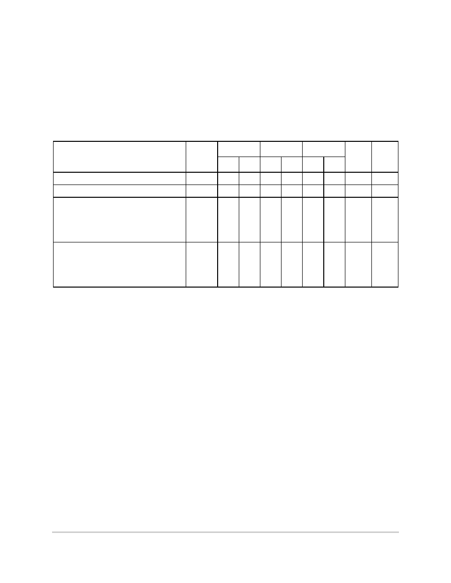
Output high voltage, I
OH
=
≠6
mA
1.8/2.0
V
OH
(L2)OV
DD
≠ 0.45
--
V
3.3
V
OH
2.4
--
V
Output low voltage, I
OL
=
6
mA
1.8/2.0
V
OL
--
0.45
V
3.3
V
OL
--
0.4
V
Notes:
1. Nominal voltages; see Table 3 for recommended operating conditions.
2. For processor bus signals, the reference is OV
DD
. L2OV
DD
is the reference for the L2 bus signals.
3. Excludes test signals (LSSD_MODE, L1_TSTCLK, L2_TSTCLK) and IEEE 1149.1 boundary scan (JTAG) signals.
Table 10. Processor Bus AC Timing Specifications
At recommended operating conditions (see Table 3)
Parameter
Symbol
300, 350, 400 MHz
Unit
Min
Max
Input Hold Times: All Inputs
t
IXKH
0.6
--
ns
Valid Times: All Outputs
t
KHOV
--
4.5
ns
Table 6. DC Electrical Specifications (continued)
At recommended operating conditions (see Table 3)
Characteristic
Nominal
Bus
Voltage
1
Symbol
Min
Max
Unit
Notes
MOTOROLA
MPC755 Part Number Specification for the
5
XPC755B
xxnnn
LD and XPC745B
xxnnn
LD Series
General Parameters
when the driver output impedance is greater than the board impedance and can cause reflected wave
switching instead of incident wave switching. The voltage level at which the step will occur is
V
step
= L2OV
DD
◊ [Z
board
/ (Z
out
+ Z
board
)]. If V
step
is less than the input high threshold voltage of the
SRAM, the SRAM will not recognize a logical high on a given signal until the reflected wave arrives. The
time delay between the arrival of the incident wave and the reflected wave is determined solely by the
propagation delay of the signal. Because of these issues, Motorola does not recommend or support the use
of the L2 bus interface of the affected part numbers described herein in 1.8 V/2.0 V mode.
Table 12. L2 Bus Interface AC Timing Specifications
At recommended operating conditions (see Table 3)
Parameter
Symbol
300 MHz
350 MHz
400 MHz
Unit
Notes
Min
Max
Min
Max
Min
Max
Setup Times: Data and parity
t
DVL2CH
1.5
--
1.5
--
1.5
--
ns
2
Input Hold Times: Data and parity
t
DXL2CH
0.5
--
0.5
--
0.5
--
ns
2
Valid Times:
All outputs when L2CR[14≠15] = 00
All outputs when L2CR[14≠15] = 01
All outputs when L2CR[14≠15] = 10
All outputs when L2CR[14≠15] = 11
t
L2CHOV
--
--
--
--
3.6
3.8
4.0
4.2
--
--
--
--
3.6
3.8
4.0
4.2
--
--
--
--
3.6
3.8
4.0
4.2
ns
3, 4
L2SYNC_IN to high impedance:
All outputs when L2CR[14≠15] = 00
All outputs when L2CR[14≠15] = 01
All outputs when L2CR[14≠15] = 10
All outputs when L2CR[14≠15] = 11
t
L2CHOZ
--
--
--
--
3.5
4.0
4.2
4.5
--
--
--
--
3.5
4.0
4.2
4.5
--
--
--
--
3.5
4.0
4.2
4.5
ns
3, 5
Notes:
2. All input specifications are measured from the midpoint of the signal in question to the midpoint voltage of the rising
edge of the input L2SYNC_IN. Input timings are measured at the pins.
3. All output specifications are measured from the midpoint voltage of the rising edge of L2SYNC_IN to the midpoint
of the signal in question. The output timings are measured at the pins. All output timings assume a purely resistive
50-
load.
4. The outputs are valid for both single-ended and differential L2CLK modes. For pipelined registered synchronous
BurstRAMs, L2CR[14≠15] = 01 or 10 is recommended. For pipelined late write synchronous BurstRAMs,
L2CR[14≠15] = 11 is recommended.
5. Guaranteed by design and characterization.
6
MPC755 Part Number Specification for the
MOTOROLA
XPC755B
xxnnn
LD and XPC745B
xxnnn
LD Series
Ordering Information
1.10 Ordering Information
1.10.1 Part Numbers Addressed by This Specification
Table 20 provides the ordering information for the MPC755 parts described in this specification.
1.10.3 Part Marking
Parts are marked as the example shown in Figure 29.
Figure 29. Part Marking for BGA Device
Table 20. Part Numbering Nomenclature
XPC
xxx
B
xx
nnn
x
x
Product
Code
Part
Identifier
Process
Descriptor
Package
Processor
Frequency
1
Application
Modifier
Revision Level
XPC
2
755
745
B = HiP4DP PX = PBGA
RX = CBGA
300
350
400
L: 2.0 V ±100 mV
0
∞
to 105
∞
C
D: 2.7; PVR = 0008 3203
Notes:
1. Processor core frequencies supported by parts addressed by this specification only. Parts addressed by other
specifications may support other maximum core frequencies.
2. The X prefix in a Motorola part number designates a "Pilot Production Prototype" as defined by Motorola SOP
3-13. These are from a limited production volume of prototypes manufactured, tested, and Q.A. inspected on
a qualified technology to simulate normal production. These parts have only preliminary reliability and
characterization data. Before pilot production prototypes may be shipped, written authorization from the
customer must be on file in the applicable sales office acknowledging the qualification status and the fact that
product changes may still occur while shipping pilot production prototypes.
BGA
MPC755B
RX400LD
MMMMMM
ATWLYYWWA
755
BGA
MPC745B
PX350LD
MMMMMM
ATWLYYWWA
745
Notes
:
CCCCC is the country of assembly. This space is left blank if parts are assembled in the United States.
MMMMMM is the 6-digit mask number.
ATWLYYWWA is the traceability code.
MOTOROLA
MPC755 Part Number Specification for the
7
XPC755B
xxnnn
LD and XPC745B
xxnnn
LD Series
Document Revision History
Document Revision History
Table B provides a revision history for this hardware specification.
Table B. Document Revision History
Revision No.
Substantive Change(s)
0≠1
Initial releases.
2
Updated document.
Corrected Section 1.4.2.4.

MPC755BLDPNS/D
HOW TO REACH US:
USA/EUROPE/LOCATIONS NOT LISTED:
Motorola Literature Distribution
P.O. Box 5405, Denver, Colorado 80217
1-303-675-2140 or 1-800-441-2447
JAPAN:
Motorola Japan Ltd.
SPS, Technical Information Center
3-20-1, Minami-Azabu Minato-ku
Tokyo 106-8573 Japan
81-3-3440-3569
ASIA/PACIFIC:
Motorola Semiconductors H.K. Ltd.
Silicon Harbour Centre, 2 Dai King Street
Tai Po Industrial Estate, Tai Po, N.T., Hong Kong
852-26668334
TECHNICAL INFORMATION CENTER:
1-800-521-6274
HOME PAGE:
http://www.motorola.com/semiconductors
DOCUMENT COMMENTS:
FAX (512) 933-2625
Attn: RISC Applications Engineering
Information in this document is provided solely to enable system and software implementers to use
Motorola products. There are no express or implied copyright licenses granted hereunder to design
or fabricate any integrated circuits or integrated circuits based on the information in this document.
Motorola reserves the right to make changes without further notice to any products herein.
Motorola makes no warranty, representation or guarantee regarding the suitability of its products
for any particular purpose, nor does Motorola assume any liability arising out of the application or
use of any product or circuit, and specifically disclaims any and all liability, including without
limitation consequential or incidental damages. "Typical" parameters which may be provided in
Motorola data sheets and/or specifications can and do vary in different applications and actual
performance may vary over time. All operating parameters, including "Typicals" must be validated
for each customer application by customer's technical experts. Motorola does not convey any
license under its patent rights nor the rights of others. Motorola products are not designed,
intended, or authorized for use as components in systems intended for surgical implant into the
body, or other applications intended to support or sustain life, or for any other application in which
the failure of the Motorola product could create a situation where personal injury or death may
occur. Should Buyer purchase or use Motorola products for any such unintended or unauthorized
application, Buyer shall indemnify and hold Motorola and its officers, employees, subsidiaries,
affiliates, and distributors harmless against all claims, costs, damages, and expenses, and
reasonable attorney fees arising out of, directly or indirectly, any claim of personal injury or death
associated with such unintended or unauthorized use, even if such claim alleges that Motorola was
negligent regarding the design or manufacture of the part.
Motorola and the Stylized M Logo are registered in the U.S. Patent and Trademark Office.
digital dna is a trademark of Motorola, Inc. All other product or service names are the property of
their respective owners. Motorola, Inc. is an Equal Opportunity/Affirmative Action Employer.
© Motorola, Inc. 2002