
Order this document by
MPC823EELE/D
Rev 0
MPC823e AC Electrical Specifications
This document contains information on a product under development. Motorola reserves the right to change or discontinue this product without notice. PowerPC
is a registered trademark of IBM Corp. and is used by Motorola under license from IBM Corp. I
2
C is a registered trademark of Philips Corporation.
”
2000 Motorola, Inc.All Rights Reserved.
This document contains detailed information on power considerations, DC/AC electrical
characteristics, and AC timing specifications for the MPC823e.
This device contains circuitry protecting against damage from high-static voltage or electrical
fields. However, it is advised that precautions be taken to avoid application of any voltages
higher than the maximum-rated voltages to this high-impedance circuit. Reliability of operation
is enhanced if unused inputs are tied to an appropriate logic voltage level (either GND or V
CC
).
Note:
Visit our website at www.motorola.com if you are using a frequency other than
25, 40, or 50MHz. Our website contains a spreadsheet that you can use to
calculate the timing for your specific system frequency.

2
MPC823e ELECTRICAL SPECIFICATIONS
MOTOROLA
MAXIMUM RATINGS (GND = 0V)
THERMAL CHARACTERISTICS
RATING
SYMBOL
VALUE
UNIT
Supply Voltage
VDDH
-0.3 to 4.0
V
VDD
-0.3 to 4.0
V
KAPWR
-0.3 to 4.0
V
VDDSYN
-0.3 to 4.0
V
Input Voltage (JTAG and GPIO)
VIN
-0.3 to 5.8
V
Input Voltage (All other pins)
VIN
-0.3 to 3.3
V
Operating Temperature
T
A
0 to 70˚
or
-40˚ to 85˚
˚C
Storage Temperature Range
T
STG
-55 to +150
˚C
NOTES:
1.
Functional operating conditions are given in
DC Electrical Characteristics (VCC
= 3.0 -
3.6 V)
. Absolute maximum ratings are stress ratings only, and functional operation at the
maxima is not guaranteed. Stress beyond those listed may affect device reliability or cause
permanent damage to the device.
2.
CAUTION
: The JTAG and GPIO input voltages cannot be more than 2.5 V greater than
supply voltage, this restriction applies also on “power-on” as well as on normal operation.
3.
5 Volt friendly inputs are inputs that tolerate 5 volts for JTAG and GPIO pins.
CHARACTERISTIC
SYMBOL
VALUE
UNIT
Thermal Resistance for BGA
q
Jc
~30
∞
C/W

MOTOROLA
MPC823e ELECTRICAL SPECIFICATIONS
3
POWER CONSIDERATIONS
The average chip-junction temperature
,
T
J
,
in
∞
C can be obtained from
T
J
= T
A
+ (P
D
•
q
JA
)
(1)
where
T
A
=
Ambient Temperature
,
•
C
q
JA
=
Package Thermal Resistance
,
Junction to Ambient
,
•
C/W
P
D
=
P
INT
+ P
I/O
P
INT
=
I
DD
x V
DD
,
Watts—Chip Internal Power
P
I/O
=
Power Dissipation on Input and Output Pins—User Determined
For most applications P
I/O
< 0.3
•
P
INT
and can be neglected. If P
I/O
is neglected
,
an approximate
relationship between P
D
and T
J
is:
P
D
=
K
’
(T
J
+ 273
•
C)
(2)
Solving equations (1) and (2) for K gives
K =
P
D
•
(T
A
+ 273
•
C) + q
JA
• P
D
2
(3)
where K is a constant pertaining to the particular part. K can be determined from equation (3)
by measuring P
D
(at equilibrium) for a known T
A
. Using this value of K
,
the values of P
D
and T
J
can be obtained by solving equations (1) and (2) iteratively for any value of T
A
.
Layout Practices
Each V
CC
pin on the MPC823e should be provided with a low-impedance path to the board’s
supply. Each GND pin should be provided with a low-impedance path to ground. The power
supply pins drive distinct groups of logic on chip. The V
CC
power supply should be bypassed to
ground using at least four 0.1
m
F bypass capacitors located as close as possible to the four
sides of the package. The capacitor leads and associated printed circuit traces connecting to
chip V
CC
and GND should be kept to less than half an inch per capacitor lead. A four-layer
board that employs two inner layers as V
CC
and GND planes should be used.
All output pins on the MPC823e have fast rise and fall times. Printed circuit (PC) trace
interconnection length should be minimized in order to minimize undershoot and reflections
caused by these fast output switching times. This recommendation particularly applies to the
address and data busses. Maximum PC trace lengths of six inches are recommended.
Capacitance calculations should consider all device loads as well as parasitic capacitances
due to the PC traces. Attention to proper PCB layout and bypassing becomes especially critical
in systems with higher capacitive loads because these loads create higher transient currents
in the V
CC
and GND circuits. Pull up all unused inputs or signals that will be inputs during reset.
Special care should be taken to minimize the noise levels on the PLL supply pins.
4
MPC823e ELECTRICAL SPECIFICATIONS
MOTOROLA
DC ELECTRICAL CHARACTERISTICS
(V
CC
= 3.0 - 3.6 V)
CHARACTERISTIC
SYMBOL
MIN
MAX
UNIT
Input High Voltage (for JTAG and GPIO)
V
IH
2.0
5.5
V
Input High Voltage (all other pins)
V
IH
2.0
3.6
V
Input Low Voltage
V
IL
GND
0.8
V
EXTAL and EXTCLK Input High Voltage
V
IHC
0.7*(V
CC
)
V
CC
+0.3
V
Input Leakage Current, V
IN
= 5.5 V
I
IN
—
±10
µA
Hi-z (Off State) Leakage Current, V
IN
= 3.5V
I
OZ
—
±10
µA
Signal Low Input Current, V
IL
= 0.8 V
I
L
±10
µA
Signal High Input Current, V
IH
= 2.0 V
I
H
±10
µA
Output High Voltage, I
OH
= –2.0 mA
,
V
DDH
= 3.0V
Except XTAL, XFC, and Open-Drain Pins
V
OH
2.4
—
V
Output Low Voltage
IOL = 2.0 mA CLKOUT
IOL = 3.2 mAA[6:31], TSIZ0/REG, TSIZ1, D(0:31), DP[0:3]/IRQ[3:6],
RD/WR, BURST, RSV/IRQ2, IP_B[0:1]/IWP[0:1]/VFLS[0:1], IP_B2/
IOIS16_B/AT2, IP_B3/IWP2/VF2, IP_B4/LWP0/VF0, IP_B5/LWP1/
VF1, IP_B6/DSDI/AT0, IP_B7/PTR/AT3, USBRXD/PA15, RXD2/
PA13, SMRXD2/L1TXDA/PA9, SMTXD2/L1RXDA/PA8, IRQ4/KR/
SPKROUT, TIN1/L1RCLKA/BRGO1/CLK1/PA7, TIN3/L1RCLKB/
TOUT1/CLK2/PA6, TIN2/L1TCLKA/BRGO2/CLK3/PA5, TIN4/
L1TCLKB/TOUT2/CLK4/PA4, LCD_A/SPISEL/PB31, SPICLK/
PB30, SPIMOSI/PB29, BRGO3/SPIMISO/PB28, BRGO1/I2CSDA/
PB27, BRGO2/I2CSCL/PB26, SMTXD1/PB25, SMRXD1/L1RXDB/
PB24, SMSYN1/SDACK1/L1TSYNCB/PB23, SMSYN2/SDACK2/
L1RSYNCB/PB22, LCD_B/L1ST1/PB19, L1ST2/RTS2/PB18,
LCD_C/L1ST3/PB17, L1ST4/L1RQA/PB16, L1ST5/L1TXDB/
DREQ1/PC15, L1ST6/RTS2/DREQ2/PC14, L1ST7/PC13, L1ST8/
L1RQA/PC12, USBRXP/PC11, USBRXN/TGATE1/PC10, CTS2/
PC9, TGATE1/CD2/PC8, USBTXP/PC7, USBTXN/PC6, SDACK1/
L1TSYNCA/PC5, L1RSYNCA/PC4, LD8/VD7/PD15, LD7/VD6/
PD14, LD6/VD5/PD13, LD5/VD4/PD12, LD4/VD3/PD11, LD3/VD2/
PD10, LD2/VD1/PD9, LD1/VD0/PD8, FRAME/VSYNC/PD5,
LCD_AC/LOE/BLANK/PD6, LD0/FIELD/PD7, LOAD/HSYNC/PD4,
SHIFT/CLK/PD3
V
OL
—
0.5
V
IOL = 5.3 mABDIP/GPL_B5, BR, BG, FRZ/IRQ6, CS[0:5], CS6/
CE1_B, CS7/CE2_B, WE0/BS_AB0/IORD, WE1/BS_AB1/IOWR,
WE2/BS_AB2/PCOE, WE3/BS_AB3/PCWE, GPL_A0/GPL_B0, OE/
GPL_A1/GPL_B1, GPL_A[2:3]/GPL_B[2:3]/CS[2:3], UPWAITA/
GPL_A4/AS, UPWAITB/GPL_B4, GPL_A5, ALE_B/DSCK/AT1,
OP2/MODCK1/STS, OP3/MODCK2/DSDO
IOL = 7.0 mA USBOE/PA14, TXD2/PA12
IOL = 8.9 mATS, TA, TEA, BI, BB, HRESET, SRESET
NOTE: Input pin voltage specifications are V
CC
= +4 V or 5.8 V, whichever is less.
AC timings are based on a 50 p
load.

MOTOROLA
MPC823e ELECTRICAL SPECIFICATIONS
5
AC ELECTRICAL CHARACTERISTICS
CLKOUT
OUTPUTS
INPUTS
INPUTS
2.0V
0.8V
2.0V
2.0V
0.8V
0.8V
2.0V
2.0V
0.8V
0.8V
2.0V
2.0V
0.8V
0.8V
2.0V
OUTPUTS
2.0V
0.8V
0.8V
2.0V
0.8V
C
D
A
B
C
D
A
B
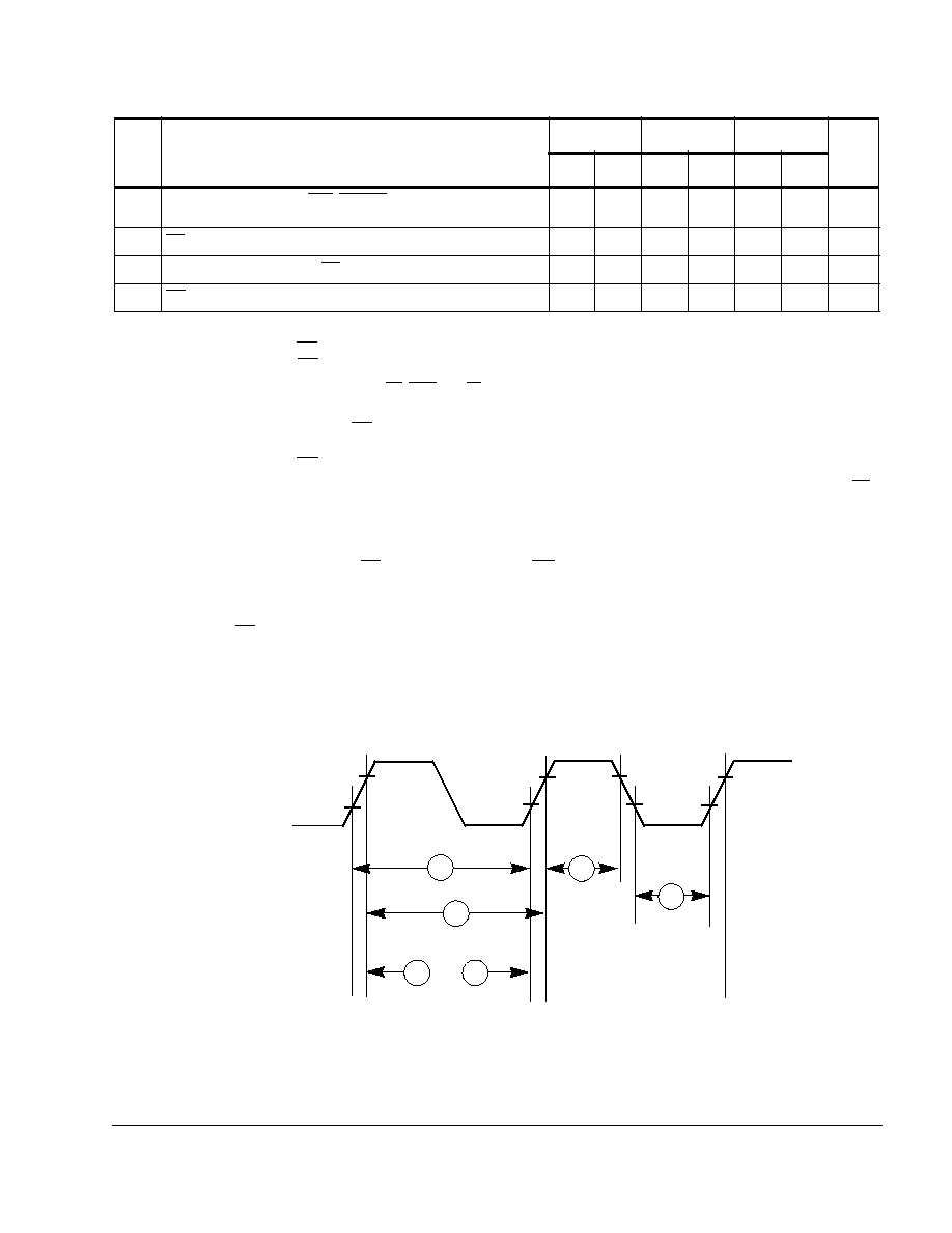
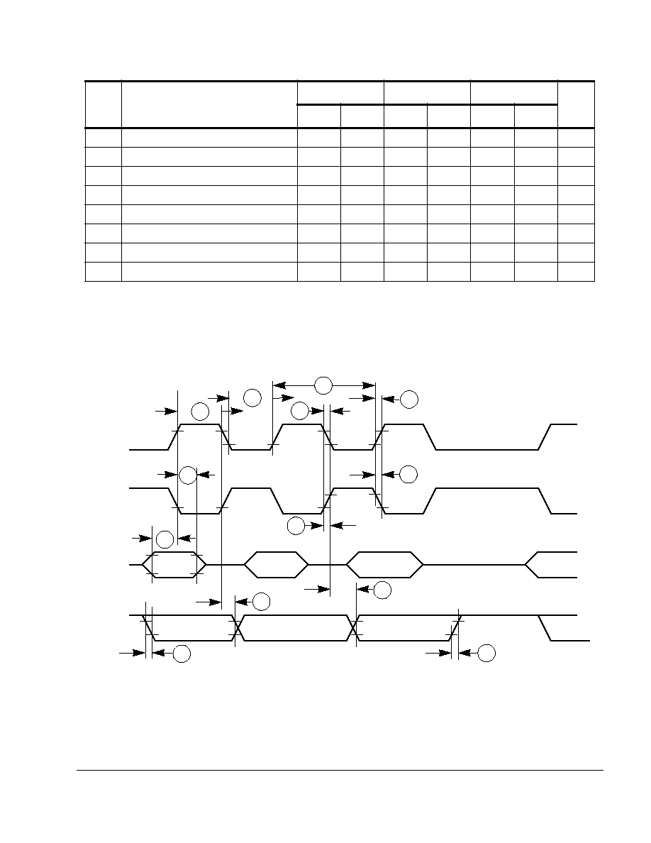
A = MAXIMUM OUTPUT DELAY SPECIFICATION
B = MINIMUM OUTPUT HOLD TIME
C = MINIMUM INPUT SETUP TIME SPECIFICATION
D = MINIMUM INPUT HOLD TIME SPECIFICATION

6
MPC823e ELECTRICAL SPECIFICATIONS
MOTOROLA
EXTERNAL BUS ELECTRICAL CHARACTERISTICS
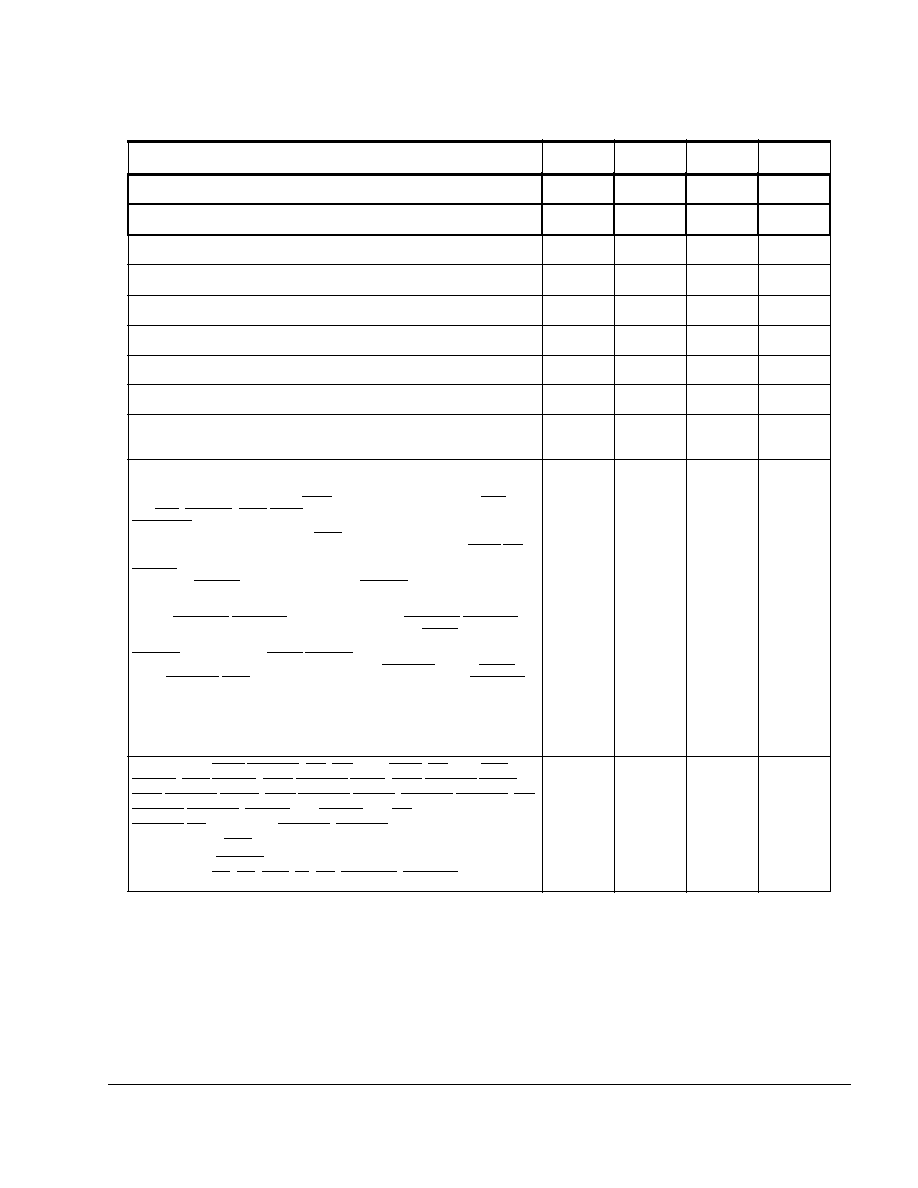
Table 1. Bus Operation Timing
NUM
CHARACTERISTIC
25MHz
40MHz
50MHz
UNIT
MIN
MAX
MIN
MAX
MIN
MAX
B1
CLKOUT Period
40
—
25
—
20
—
ns
B1a
EXTCLK to CLKOUT Phase Skew (EXTCLK>15MHz and
MF
£
2)
-0.9
0.9
-0.9
0.9
-0.9
0.9
ns
B1b
EXTCLK to CLKOUT Phase Skew (EXTCLK>10MHz and
MF
£ 10)
-2.3
2.3
-2.3
2.3
-2.3
2.3
ns
B1c
CLKOUT Phase Jitter (EXTCLK>15MHz and MF
£2)
-0.6
0.6
-0.6
0.6
-0.6
0.6
ns
B1d
CLKOUT Phase Jitter (EXTCLK>10MHz and MF
£10)
-2
2
-2
2
-2
2
ns
B1e
CLKOUT Frequency Jitter (MF<10)
—
0.5
—
0.5
—
0.5
%
B1f
CLKOUT Frequency Jitter (10<MF<500)
—
2
—
2
—
2
%
B1g
CLKOUT Frequency Jitter (MF>500)
—
3
—
3
—
3
%
B1h
Frequency Jitter on EXTCLK
—
0.5
—
0.5
—
0.5
%
B2
Clock Pulse Width Low
16
—
10
—
8
—
ns
B3
Clock Pulse Width High
16
—
10
—
8
—
ns
B4
CLKOUT Rise Time
—
4
—
4
—
4
ns
B5
CLKOUT Fall Time
—
4
—
4
—
4
ns
B6
N/A (Used on Interactive Spreadsheet)
B7
CLKOUT to A(6:31), RD/WR, BURST, D(0:31), DP(0:3)
Invalid
10
—
5
—
5
—
ns
B7a
CLKOUT to TSIZ(0:1),REG, RSV, AT(0:3),BDIP, PTR Invalid
10
—
5
—
5
—
ns
B7b
CLKOUT to BR, BG, FRZ, VFLS(0:1), VF(0:2), IWP(0:2),
LWP(0:1), STS Invalid
10
—
5
—
5
—
ns
B8
CLKOUT to A(6:31), RD/WR, BURST, D(0:31), DP(0:3) Valid
10
19
5
13
5
12
ns
B8a
CLKOUT to TSIZ(0:1),REG, RSV, AT(0:3), BDIP, PTR Valid
10
19
5
13
5
12
ns
B8b
CLKOUT to BR, BG, VFLS(0:1), VF(0:2), IWP(0:2), FRZ,
LWP(0:1), STS Valid
10
19
5
13
5
12
ns
B9
CLKOUT to A(6:31), RD/WR, BURST, D(0:31), DP(0:3),
TSIZ(0:1),REG, RSV, AT(0:3), PTR Hi Z
10
19
5
13
5
12
ns
B10
N/A
B11
CLKOUT to TS, BB Assertion
10
19
5
12.25
5
12.25
ns
B11a
CLKOUT to TA, BI Assertion (when driven by the
Memory Controller or PCMCIA Interface)
2.5
11
2.5
9.25
2.5
9.25
ns
B12
CLKOUT to TS, BB Negation
10
19
5
13
5
12
ns
B12a
CLKOUT to TA, BI Negation (when driven by the
Memory Controller or PCMCIA Interface)
2.5
11
2.5
11
2.5
11
ns
B13
CLKOUT to TS, BB Hi Z
10
24
5
21
5
19
ns

MOTOROLA
MPC823e ELECTRICAL SPECIFICATIONS
7
B13a
CLKOUT to TA, BI Hi Z (When Driven by the Memory
Controller or PCMCIA Interface)
2.5
15
2.5
15
2.5
16
ns
B14
CLKOUT to TEA Assertion
2.5
11
2.5
11
2.5
10
ns
B15
CLKOUT to TEA Hi Z
2.5
15
2.5
15
2.5
15
ns
B16
TA, BI Valid to CLKOUT (Setup Time)
9.75
—
9.75
—
9.75
—
ns
B16a
TEA, KR, RETRY Valid to CLKOUT (Setup Time)
11
—
10
—
10
—
ns
B16b
BB, BG, BR Valid to CLKOUT (Setup Time)
8.5
—
8.5
—
8.5
—
ns
B17
CLKOUT to TA, TEA, BI , BB, BG, BR Valid (Hold Time)
1
—
1
—
1
—
ns
B17a
CLKOUT to KR, RETRY Valid (Hold Time)
2
—
2
—
2
—
ns
B18
D(0:31), DP(0:3) Valid to CLKOUT Rising Edge (Setup Time)
6
—
6
—
6
—
ns
B19
CLKOUT Rising Edge to D(0:31), DP(0:3) Valid (Hold Time)
2
—
2
—
2
—
ns
B20
D(0:31), DP(0:3) Valid to CLKOUT Falling Edge (Setup Time)
4
—
4
—
4
—
ns
B21
CLKOUT Falling Edge to D(0:31), DP(0:3) Valid (Hold Time)
2
—
2
—
2
—
ns
B22
CLKOUT Rising Edge to CS Asserted -GPCM- ACS = 00
10
20
5
13
5
13
ns
B22a
CLKOUT Falling Edge to CS Asserted -GPCM- ACS = 10,
TRLX = 0
—
10
—
8
—
8
ns
B22b
CLKOUT Falling Edge to CS Asserted -GPCM- ACS = 11,
TRLX = 0, EBDF = 0
10
20
5
13
5
13
ns
B22c
CLKOUT Falling Edge to CS Asserted -GPCM- ACS = 11,
TRLX = 0, EBDF = 1
14
25
7
16
7
16
ns
B23
CLKOUT Rising Edge to CS Negated -GPCM-Read Access -
GPCM-Write Access, ACS=00, TRLX=0, CSNT=0
3
10
2
8
2
8
ns
B24
A(6:31) to CS Asserted -GPCM- ACS = 10, TRLX = 0
8
—
3
—
3
—
ns
B24a
A(6:31) to CS Asserted -GPCM- ACS = 11, TRLX = 0
18
—
8
—
8
—
ns
B25
CLKOUT Rising Edge to OE, WE(0:3) Asserted
—
11
—
9
—
9
ns
B26
CLKOUT Rising Edge to OE Negated
3
11
2
9
2
9
ns
B27
A(6:31) to CS Asserted -GPCM- ACS = 10, TRLX = 1
48
—
23
—
23
—
ns
B27a
A(6:31) to CS Asserted -GPCM- ACS = 11, TRLX = 1
58
—
28
—
28
—
ns
B28
CLKOUT Rising Edge to WE(0:3) Negated -GPCM-Write
Access CSNT = ‘0‘
—
11
—
9
—
9
ns
B28a
CLKOUT Falling Edge to WE(0:3) Negated -GPCM-Write
Access TRLX = ‘0’, CSNT = ‘1’, EBDF=0
10
20
5
13
5
13
ns
B28b
CLKOUT Falling Edge to CS Negated -GPCM-Write Access
TRLX = ‘0’, CSNT = ‘1’, ACS = ‘10’ or ACS=’11’, EBDF = 0
—
20
—
13
—
13
ns
Table 1. Bus Operation Timing (Continued)
NUM
CHARACTERISTIC
25MHz
40MHz
50MHz
UNIT
MIN
MAX
MIN
MAX
MIN
MAX

8
MPC823e ELECTRICAL SPECIFICATIONS
MOTOROLA
B28c
CLKOUT Falling Edge to WE(0:3) Negated -GPCM-Write
Access TRLX = ‘0’, CSNT = ‘1’, EBDF=1
14
25
7
16
7
16
ns
B28d
CLKOUT Falling Edge to CS Negated -GPCM-Write Access
TRLX = ‘0’, CSNT = ‘1’, ACS = ‘10’ or ACS=’11’, EBDF = 1
—
25
—
16
—
16
ns
B29
WE(0:3) Negated to D(0:31), DP(0:3) Hi Z -GPCM- Write
Access, CSNT = ‘0’
8
—
3
—
3
—
ns
B29a
WE(0:3) Negated to D(0:31), DP(0:3) Hi Z -GPCM- Write
Access, TRLX = ‘0’, CSNT = ‘1’, EBDF = 0
18
—
8
—
8
—
ns
B29b
CS Negated to D(0:31), DP(0:3) Hi Z -GPCM- Write Access,
ACS = ‘00’, TRLX = ‘0’ & CSNT = ‘0’
8
—
3
—
3
—
ns
B29c
CS Negated to D(0:31), DP(0:3) Hi Z -GPCM- Write Access,
TRLX = ‘0’, CSNT = ‘1’, ACS = ‘10’ or ACS=’11’, EBDF = 0
18
—
8
—
8
—
ns
B29d
WE(0:3) Negated to D(0:31), DP(0:3) Hi Z -GPCM- Write
Access, TRLX = ‘1’, CSNT = ‘1’, EBDF = 0
58
—
28
—
28
—
ns
B29e
CS Negated to D(0:31), DP(0:3) Hi Z -GPCM- Write Access,
TRLX = ‘1’, CSNT = ‘1’, ACS = ‘10’ or ACS=’11’, EBDF = 0
58
—
28
—
28
—
ns
B29f
WE(0:3) Negated to D(0:31), DP(0:3) Hi Z -GPCM- Write
Access, TRLX = ‘0’, CSNT = ‘1’, EBDF = 1
12
—
5
—
5
—
ns
B29g
CS Negated to D(0:31), DP(0:3) Hi Z -GPCM- Write Access,
TRLX = ‘0’, CSNT = ‘1’, ACS = ‘10’ or ACS=’11’, EBDF = 1
12
—
5
—
5
—
ns
B29h
WE(0:3) Negated to D(0:31), DP(0:3) Hi Z -GPCM- Write
Access, TRLX = ‘1’, CSNT = ‘1’, EBDF = 1
52
—
24
—
24
—
ns
B29i
CS Negated to D(0:31), DP(0:3) Hi Z -GPCM- Write Access,
TRLX = ‘1’, CSNT = ‘1’, ACS = ‘10’ or ACS=’11’, EBDF =1
52
—
24
—
24
—
ns
B30
CS, WE(0:3) Negated to A(6:31) invalid -GPCM- Write
Access.
8
—
3
—
3
—
B30a
WE(0:3) Negated to A(6:31) Invalid -GPCM- Write Access,
TRLX=’0’, CSNT = '1’. CS Negated to A(6:31) Invalid -GPCM-
Write Access, TRLX=’0’, CSNT = '1’, ACS = 10,ACS = =’11’,
EBDF = 0
18
—
8
—
8
—
ns
B30b
WE(0:3) Negated to A(6:31)Invalid -GPCM- Write Access,
TRLX=’1’, CSNT = '1’. CS Negated to A(6:31)Invalid -GPCM-
Write Access, TRLX=’1’, CSNT = '1’, ACS = 10,ACS = =’11’,
EBDF = 0
58
—
28
—
28
—
ns
B30c
WE(0:3) Negated to A(6:31) Invalid -GPCM- Write Access,
TRLX=’0’, CSNT = '1’. CS Negated to A(6:31) Invalid -GPCM-
Write Access, TRLX=’0’, CSNT = '1’, ACS = 10 ,ACS = =’11’,
EBDF = 1
12
—
4
—
4
—
ns
B30d
WE(0:3) Negated to A(6:31) Invalid -GPCM- Write Access,
TRLX=’1’, CSNT = '1’. CS Negated to A(6:31) Invalid -GPCM-
Write Access, TRLX=’1’, CSNT = '1’, ACS = 10,ACS = =’11’,
EBDF = 1
52
—
24
—
24
—
ns
B31
CLKOUT Falling Edge to CS valid as requested by CST4 in
the corresponding word of the UPM
1.5
10
1.5
8
1.5
8
ns
Table 1. Bus Operation Timing (Continued)
NUM
CHARACTERISTIC
25MHz
40MHz
50MHz
UNIT
MIN
MAX
MIN
MAX
MIN
MAX

MOTOROLA
MPC823e ELECTRICAL SPECIFICATIONS
9
B31a
CLKOUT Falling Edge to CS valid as requested by CST1 in
the corresponding word of the UPM, EBDF = 0
10
20
5
13
5
13
ns
B31b
CLKOUT Rising Edge to CS valid as requested by CST2 in
the corresponding word of the UPM
1.5
10
1.5
8
1.5
8
ns
B31c
CLKOUT Rising Edge to CS valid as requested by CST3 in
the corresponding word of the UPM
10
20
5
13
5
13
ns
B31d
CLKOUT Falling Edge to CS valid as requested by CST1 in
the corresponding word of the UPM, EBDF = 1
10
25
5
16
5
16
ns
B32
CLKOUT Falling Edge to BS valid as requested by BST4 in
the corresponding word of the UPM
1.5
10
1.5
8
1.5
8
ns
B32a
CLKOUT Falling Edge to BS valid as requested by BST1 in
the corresponding word of the UPM, EBDF = 0
10
20
5
13
5
13
ns
B32b
CLKOUT Rising Edge to BS valid as requested by BST2 in the
corresponding word of the UPM
1.5
10
1.5
8
1.5
8
ns
B32c
CLKOUT Rising Edge to BS valid as requested by BST3 in the
corresponding word of the UPM
10
20
5
13
5
13
ns
B32d
CLKOUT Falling Edge to BS valid as requested by BST1 in
the corresponding word of the UPM, EBDF = 1
10
25
5
16
5
16
ns
B33
CLKOUT Falling Edge to GPL valid as requested by GxT4 in
the corresponding word of the UPM
1.5
10
1.5
8
1.5
8
ns
B33a
CLKOUT Rising Edge to GPL valid as requested by GxT3 in
the corresponding word of the UPM
10
20
5
13
5
13
ns
B34
A(6:31) and D(0:31) to CS valid as requested by CST4 in the
corresponding word of the UPM
8
—
3
—
3
—
ns
B34a
A(6:31) and D(0:31) to CS valid as requested by CST1 in the
corresponding word of the UPM
18
—
8
—
8
—
ns
B34b
A(6:31) and D(0:31) to CS valid as requested by CST2 in the
corresponding word of the UPM
28
—
13
—
13
—
ns
B35
A(6:31) and D(0:31) to BS valid as requested by BST4 in the
corresponding word of the UPM
8
—
3
—
3
—
ns
B35a
A(6:31) and D(0:31) to BS valid as requested by BST1 in the
corresponding word of the UPM
18
—
8
—
8
—
ns
B35b
A(6:31) and D(0:31) to BS valid as requested by BST2 in the
corresponding word of the UPM
28
—
13
—
13
—
ns
B36
A(6:31) and D(0:31) to GPL valid as requested by GxT4 in the
corresponding word of the UPM
8
—
3
—
3
—
ns
B37
UPWAIT Valid to CLKOUT Falling Edge
6
—
6
—
6
—
ns
B38
CLKOUT Falling Edge to UPWAIT Valid
1
—
1
—
1
—
ns
B39
AS Valid to CLKOUT Rising Edge
9
—
7
—
7
—
ns
Table 1. Bus Operation Timing (Continued)
NUM
CHARACTERISTIC
25MHz
40MHz
50MHz
UNIT
MIN
MAX
MIN
MAX
MIN
MAX
10
MPC823e ELECTRICAL SPECIFICATIONS
MOTOROLA
B40
A(6:31), TSIZ(0:1), RD/WR, BURST, Valid to CLKOUT Rising
Edge
9
—
7
—
7
—
ns
B41
TS Valid to CLKOUT Rising Edge (Setup Time)
9
—
7
—
7
—
ns
B42
CLKOUT Rising Edge to TS Valid (Hold Time)
2
—
2
—
2
—
ns
B43
AS Negation to Memory Controller Signals Negation
—
13
—
13
—
13
ns
NOTES:
1.
The timing for BR output is relevant when the MPC823e is selected to work with the external bus arbiter.
The timing for BG output is relevant when the MPC823e is selected to work with the internal bus arbiter.
2.
The setup times required for TA, TEA and BI are relevant only when they are supplied by an external device
(and not when the memory controller or the PCMCIA interface drive them).
3.
The timing required for BR input is relevant when the MPC823e is selected to work with the internal bus
arbiter.
The timing for BG input is relevant when the MPC823e is selected to work with the external bus arbiter.
4.
The D(0:31) and DP(0:3) input timings B18 and B19 refer to the rising edge of the CLKOUT in which the TA
input signal is asserted.
5.
The D(0:31) and DP(0:3) input timings B20 and B21 refer to the falling edge of the CLKOUT. This timing is
valid only under control of the UPM in the memory controller.
6.
The timing B30 refers to CS when ACS = ‘00’ and to WE(0:3) when CSNT = ‘0’.
7.
The signal UPWAIT is considered asynchronous to the CLKOUT and synchronized internally. The timings
speciÞed in B37 and B38 are speciÞed to enable the freeze of the UPM output signals.
8.
The AS signal is considered asynchronous to the CLKOUT signal.
Figure 1. External Clock Timing Diagram
Table 1. Bus Operation Timing (Continued)
NUM
CHARACTERISTIC
25MHz
40MHz
50MHz
UNIT
MIN
MAX
MIN
MAX
MIN
MAX
CLKOUT
B1
B1
B4
B5
B3
B2

MOTOROLA
MPC823e ELECTRICAL SPECIFICATIONS
11
Figure 2. Synchronous Output Signals Timing Diagram
CLKOUT
OUTPUT
SIGNALS
OUTPUT
SIGNALS
OUTPUT
SIGNALS
B8
B9
B9
B8a
B7a
B7
B7b
B8b

12
MPC823e ELECTRICAL SPECIFICATIONS
MOTOROLA
Figure 3. Synchronous Active Pull-Up and Open-Drain
Outputs Signals Timing Diagram
CLKOUT
TS, BB
TEA
TA, BI
B11
B13
B13a
B12
B12a
B11a
B14
B15

MOTOROLA
MPC823e ELECTRICAL SPECIFICATIONS
13
Figure 4. Synchronous Input Signals Timing Diagram
CLKOUT
TA, BI, TEA
TEA, RETRY, KR
BB, BG, BR
B16
B16a
B16b
B17
B17a
B17

14
MPC823e ELECTRICAL SPECIFICATIONS
MOTOROLA
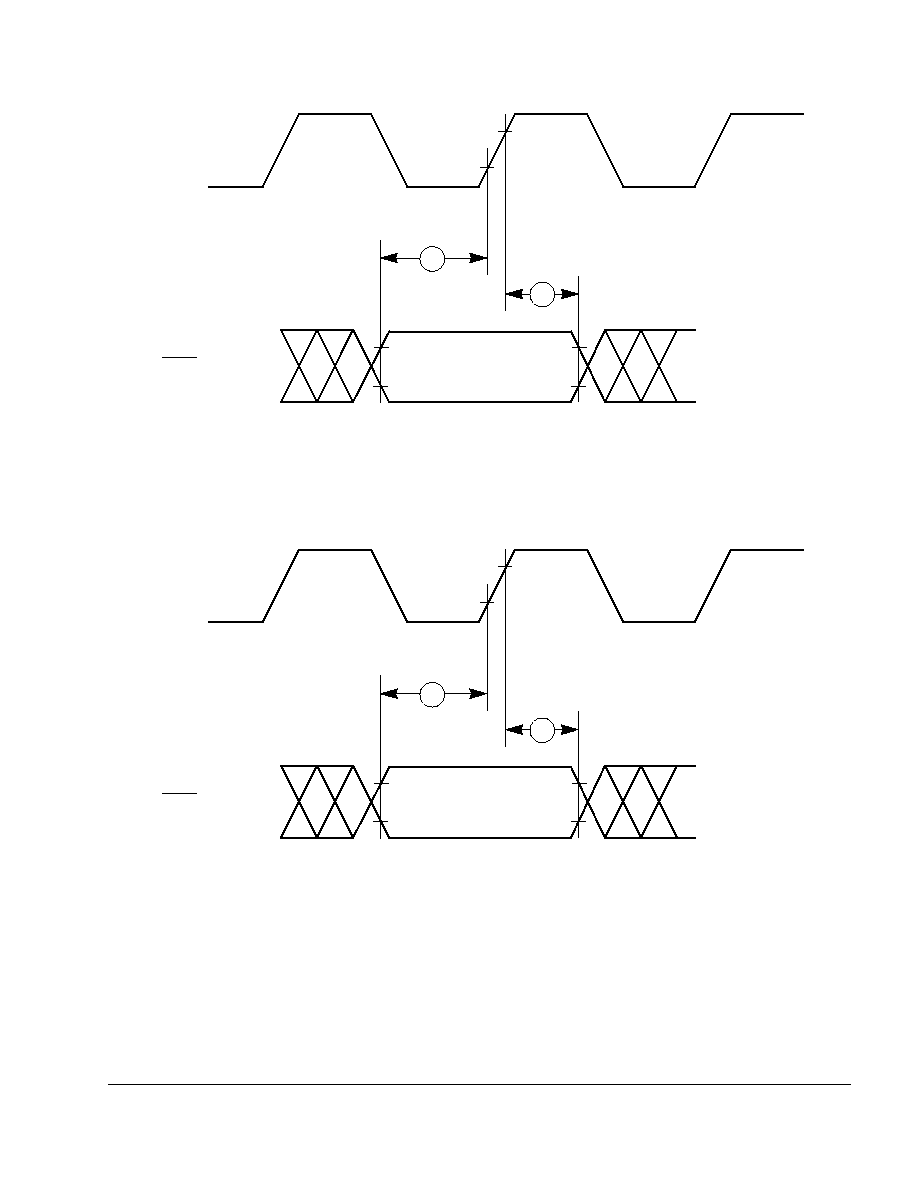
Figure 5. Input Data In Normal Case Timing Diagram
Figure 6. Input Data When Controlled by the UPM Timing Diagram
CLKOUT
TA
D(0:31),
DP(0:3)
B16
B18
B19
B17
TA
D(0:31),
DP(0:3)
CLKOUT
B20
B21

MOTOROLA
MPC823e ELECTRICAL SPECIFICATIONS
15
Figure 7. External Bus Read Timing Diagram (GPCM Controlled–ACS = ‘00’)
Figure 8. External Bus Read Timing Diagram (GPCM Controlled–TRLX = ‘0’, ACS = ‘10’)
CLKOUT
B11
TS
CSx
OE
WE(0:3)
D(0:31),
DP(0:3)
A(6:31)
B8
B22a
B28
B26
B18
B12
B23
B19
B25
CLKOUT
TS
A(6:31)
B11
CSx
OE
D(0:31),
DP(0:3)
B8
B12
B19
B25
B23
B22b
B18
B24a
B26
B22c

16
MPC823e ELECTRICAL SPECIFICATIONS
MOTOROLA
Figure 9. External Bus Read Timing Diagram
(GPCM Controlled–TRLX = ‘0’, ACS = ‘11’)
CLKOUT
TS
A(6:31)
B11
CSx
OE
D(0:31),
DP(0:3)
B12
B26
B19
B25
B23
B22b
B18
B24a
B22c
B8

MOTOROLA
MPC823e ELECTRICAL SPECIFICATIONS
17
Figure 10. External Bus Read Timing Diagram
(GPCM Controlled–TRLX = ‘1’, ACS = ‘10’, ACS = ‘11’)
CLKOUT
TS
A(6:31)
CSx
OE
D(0:31),
DP(0:3)
B22a
B18
B19
B27
B27a
B22b
B12
B26
B23
B11
B8
B22c
18
MPC823e ELECTRICAL SPECIFICATIONS
MOTOROLA
Figure 11. External Bus Write Timing Diagram
(GPCM Controlled–TRLX = ‘0’, CSNT = ‘0’)
CLKOUT
TS
A(6:31)
CSx
WE
(0:3)
D(0:31),
DP(0:3)
B8
OE
B12
B8
B11
B22
B28
B30
B23
B29b
B26
B29
B9
B25

MOTOROLA
MPC823e ELECTRICAL SPECIFICATIONS
19
Figure 12. External Bus Write Timing Diagram
(GPCM Controlled–TRLX = ‘0’, CSNT = ‘1’)
CLKOUT
TS
A(6:31)
CSx
WE(0:3)
D(0:31),
DP(0:3)
OE
B22
B11
B12
B30
B28c
B9
B30a
B28d
B25
B8
B23
B28b
B29g
B29c
B29f
B29a
B28a
B8
B26

20
MPC823e ELECTRICAL SPECIFICATIONS
MOTOROLA
Figure 13. External Bus Write Timing Diagram
(GPCM Controlled–TRLX = ‘1’, CSNT = ‘1’)
CLKOUT
TS
A(6:31)
CSx
WE
(0:3)
D(0:31),
DP(0:3)
OE
B22
B11
B8
B12
B30d
B30b
B23
B28d
B29e
B29h
B29d
B29b
B28c
B28a
B9
B8
B26
B25
B28b
B29f

MOTOROLA
MPC823e ELECTRICAL SPECIFICATIONS
21
Figure 14. External Bus Timing Diagram (UPM-Controlled Signals)
CLKOUT
A(6:31)
GPLA(0:5),
GPLB(0:5)
CSx
BS_AB(0:3)
B8
B31
B31d
B31a
B31b
B31c
B32c
B32b
B33a
B36
B33
B35b
B35a
B35
B32
B32a
B32d
B34b
B34a
B34

22
MPC823e ELECTRICAL SPECIFICATIONS
MOTOROLA
Figure 15. Asynchronous UPWAIT Asserted Detection in UPM
Handled Cycles Timing Diagram
CLKOUT
UPWAIT
CSx
BS_AB(0:3)
GPLA(0:5),
GPLB(0:5)
B37
B38

MOTOROLA
MPC823e ELECTRICAL SPECIFICATIONS
23
Figure 16. Asynchronous UPWAIT Negated Detection in UPM
Handled Cycles Timing Diagram
Figure 17. Synchronous External Master Access Timing Diagram
(GPCM Handled–ACS = ‘00’)
CLKOUT
UPWAIT
CSx
BS_AB(0:3)
GPLA(0:5),
GPLB(0:5)
B37
B38
CLKOUT
TS
A(6:31), TSIZ(0:1),
CSx
RD/WR, BURST
B40
B41
B42
B22

24
MPC823e ELECTRICAL SPECIFICATIONS
MOTOROLA
Figure 18. Asynchronous External Master Memory Access Timing Diagram
(GPCM Controlled–ACS = ’00’)
Figure 19. Asynchronous External Master Timing Diagram
(Control Signals Negation Time)
CLKOUT
AS
A(6:31),
CSx
TSIZ(0:1),
RD/WR
B40
B39
B22
AS
CSx,
WE(0:3),
OE, GPLx,
BS(0:3),
B43

MOTOROLA
MPC823e ELECTRICAL SPECIFICATIONS
25
Table 2. Interrupt Timing
NUM
CHARACTERISTIC
25MHZ
40MHZ
50MHZ
UNIT
MIN
MAX
MIN
MAX
MIN
MAX
I39
IRQx valid to CLKOUT rising edge (setup time)
6
—
6/6
—
6/6
—
ns
I40
IRQx hold time after CLKOUT
2
—
2/2
—
2/2
—
ns
I41
IRQx pulse width low
3
—
3/3
—
3/3
—
ns
I42
IRQx pulse width high
3
—
3/3
—
3/3
—
ns
I43
IRQx edge to edge time
160
—
80/80
—
80/80
—
ns
NOTES:
1.
The timings I39 and I40 describe the testing conditions under which the IRQ lines are tested when defined as
level sensitive. The IRQ lines are synchronized internally and do not have to be asserted or negated with
reference to the CLKOUT.
2.
The timings I41 and I42 are speciÞed to allow the correct function of the IRQ lines detection circuitry, and has
no direct relation with the total system interrupt latency that the MPC823e can support.
Figure 20. Interrupt Detection Timing Diagram
for External Level-Sensitive Lines
CLKOUT
IRQx
I39
I40

26
MPC823e ELECTRICAL SPECIFICATIONS
MOTOROLA
Figure 21. Interrupt Detection Timing Diagram
for External Edge-Sensitive Lines
CLKOUT
IRQx
I39
I43
I42
I41
I43

MOTOROLA
MPC823e ELECTRICAL SPECIFICATIONS
27
Table 3. PCMCIA Timing
NUM
CHARACTERISTIC
25MHZ
40MHZ
50MHZ
UNIT
MIN
MAX
MIN
MAX
MIN
MAX
P44
A(6:31), REG valid to PCMCIA strobe asserted
28
—
13
—
13
—
ns
P45
A(6:31), REG valid to ALE negation
38
—
18
—
18
—
ns
P46
CLKOUT to REG valid
10
19
5
13
5
13
ns
P47
CLKOUT to REG invalid
11
—
6
—
6
—
ns
P48
CLKOUT to CE1, CE2 asserted
10
19
5
13
5
13
ns
P49
CLKOUT to CE1, CE2 negated
10
19
5
13
5
13
ns
P50
CLKOUT to PCOE, IORD, PCWE, IOWR assert
time
—
12
—
11
—
11
ns
P51
CLKOUT to PCOE, IORD, PCWE, IOWR negate
time
3
12
2
11
2
11
ns
P52
CLKOUT to ALE assert time
10
19
5
13
5
13
ns
P53
CLKOUT to ALE negate time
—
19
—
13
—
13
ns
P54
PCWE, IOWR negated to D(0:31) invalid
8
—
3
—
3
—
ns
P55
WAIT_B valid to CLKOUT rising edge
8
—
8
—
8
—
ns
P56
CLKOUT rising edge to WAIT_B invalid
2
—
2
—
2
—
ns
NOTES:
1.
PSST = 1. Otherwise, add PSST times cycle time.
2.
PSHT = 0. Otherwise, add PSHT times cycle time.
3.
These synchronous timings deÞne when the WAIT_B signal is detected in order to freeze (or relieve) the
PCMCIA current cycle. The WAIT_B assertion will be effective only if it is detected two cycles before the PSL
timer expiration.

28
MPC823e ELECTRICAL SPECIFICATIONS
MOTOROLA
Figure 22. PCMCIA Access Cycles Timing Diagram (External Bus Read)
CLKOUT
TS
A(0:31)
REG
CE[1:2]
PCOE,
IORD
ALE
D(0:31)
PCOE,
P44
P45
P46
P48
P52
P50
P53
B18
P47
P49
P51
P52
B19

MOTOROLA
MPC823e ELECTRICAL SPECIFICATIONS
29
Figure 23. PCMCIA Access Cycles Timing Diagram (External Bus Write)
CLKOUT
TS
A[0:31]
REG
CE[1:2]
PCOE,
IORD
ALE
D[0:31]
P44
P45
P46
P50
P53
P52
P48
B8
B9
P54
P52
P51
P49
P47
30
MPC823e ELECTRICAL SPECIFICATIONS
MOTOROLA
Figure 24. PCMCIA Wait Signals Detection Timing Diagram
Figure 25. PCMCIA Wait Signals Detection Timing Diagram
CLKOUT
WAITx
P55
P56
CLKOUT
WAITx
P55
P56

MOTOROLA
MPC823e ELECTRICAL SPECIFICATIONS
31
Table 4. PCMCIA Port Timing
NUM
CHARACTERISTIC
25MHZ
40MHZ
50MHZ
UNIT
MIN
MAX
MIN
MAX
MIN
MAX
P57
CLKOUT to OPx Valid
—
25
—
19
—
19
ns
P58
HRESET negated to OPx drive
30
—
18
—
18
—
ns
P59
IP_Bx valid to CLKOUT Rising Edge
6
—
5
—
5
—
ns
P60
CLKOUT Rising Edge to IP_Bx invalid
2
—
1
—
1
—
ns
NOTE: *OP2 and OP3 only.
Figure 26. PCMCIA Output Port Timing Diagram
Figure 27. PCMCIA Input Port Timing Diagram
CLKOUT
OUTPUT
SIGNALS
HRESET
OP2, OP3
P58
P57
INPUT
SIGNALS
CLKOUT
P59
P60

32
MPC823e ELECTRICAL SPECIFICATIONS
MOTOROLA
Table 5. Debug Port Timing
NUM
CHARACTERISTIC
25MHZ
40MHZ
50MHZ
UNIT
MIN
MAX
MIN
MAX
MIN
MAX
D61
DSCK cycle time
120
—
60
—
60
—
ns
D62
DSCK clock pulse width
50
—
25
—
25
—
ns
D63
DSCK rise and fall times
0
3
0
3
0
3
ns
D64
DSDI input data setup time
8
—
8
—
8
—
ns
D65
DSDI data hold time
5
—
5
—
5
—
ns
D66
DSCK low to DSDO data valid
0
15
0
15
0
15
ns
D67
DSCK low to DSDO invalid
0
2
0
2
0
2
ns
Figure 28. Debug Port Clock Input Timing Diagram
CLKOUT
D61
D61
D63
D63
D62
D62
MOTOROLA
MPC823e ELECTRICAL SPECIFICATIONS
33
Figure 29. Debug Port Timing Diagram
DSCK
DSDI
DSDO
D64
D65
D66
D67

34
MPC823e ELECTRICAL SPECIFICATIONS
MOTOROLA
Table 6. Reset Timing
NUM
CHARACTERISTIC
25MHZ
40MHZ
50MHZ
UNIT
MIN
MAX
MIN
MAX
MIN
MAX
R68
CLKOUT to HRESET high impedance
—
20
—
20
—
20
ns
R69
CLKOUT to SRESET high impedance
—
20
—
20
—
20
ns
R70
RSTCONF pulse width
680
—
425
—
340
—
ns
R71
N/A
R72
Configuration data to HRESET rising edge setup
time
650
—
425
—
350
—
ns
R73
Configuration data to RSTCONF rising edge setup
time
650
—
425
—
350
—
ns
R74
Configuration data hold time after RSTCONF
negation
0
—
0
—
0
—
ns
R75
Configuration data hold time after HRESET negation
0
—
0
—
0
—
ns
R76
HRESET and RSTCONF asserted to data out drive
—
25
—
25
—
25
ns
R77
RSTCONF negated to data out high impedance
—
25
—
25
—
25
ns
R78
CLKOUT of last rising edge before chip three-states
HRESET to data out high impedance
—
25
—
25
—
25
ns
R79
DSDI and DSCK setup
120
—
75
—
60
—
ns
R80
DSDI and DSCK hold time
0
—
0
—
0
—
ns
R81
SRESET negated to CLKOUT rising edge for DSDI
and DSCK sample
320
—
200
—
160
—
ns

MOTOROLA
MPC823e ELECTRICAL SPECIFICATIONS
35
Figure 30. Reset Timing Diagram (Configuration from Data Bus)
Figure 31. Reset Timing Diagram–MPC823e Data Bus Weak Drive During Configuration
HRESET
RSTCONF
D(0:31) (IN)
R75
R74
R73
R76
R71
CLKOUT
HRESET
D(0:31) (OUT)
RSTCONF
(WEAK)
R77
R78
R79
R69
36
MPC823e ELECTRICAL SPECIFICATIONS
MOTOROLA
Figure 32. Reset Timing Diagram–Debug Port Configuration
CLKOUT
SRESET
DSCK, DSDI
R70
R82
R80
R81
R81
R80

MOTOROLA
MPC823e ELECTRICAL SPECIFICATIONS
37
Table 7. JTAG Timing
NUM
CHARACTERISTIC
25MHZ
40MHZ
50MHZ
UNIT
MIN
MAX
MIN
MAX
MIN
MAX
J82
TCK cycle time
100
—
100
—
100
—
ns
J83
TCK clock pulse width measured at 1.5V
40
—
40
—
40
—
ns
J84
TCK rise and fall times
0
10
0
10
0
10
ns
J85
TMS, TDI data setup time
5
—
5
—
5
—
ns
J86
TMS, TDI data hold time
25
—
25
—
25
—
ns
J87
TCK low to TDO data valid
—
27
—
27
—
27
ns
J88
TCK low to TDO data invalid
0
—
0
—
0
—
ns
J89
TCK low to TDO high impedance
—
20
—
20
—
20
ns
J90
TRST assert time
100
—
100
—
100
—
ns
J91
TRST setup time to TCK low
40
—
40
—
40
—
ns
J92
TCK falling edge to output valid
—
50
—
50
—
50
ns
J93
TCK falling edge to ouput valid out of high impedance
—
50
—
50
—
50
ns
J94
TCK falling edge to output high impedance
—
50
—
50
—
50
ns
J95
Boundary scan input valid to TCK rising edge
50
—
50
—
50
—
ns
J96
TCK rising edge to boundary scan input invalid
50
—
50
—
50
—
ns
Figure 33. JTAG Test Clock Input Timing Diagram
TCK
J84
J83
J82
J82
J84
J83

38
MPC823e ELECTRICAL SPECIFICATIONS
MOTOROLA
Figure 34. JTAG–Test Access Port Timing Diagram
Figure 35. JTAG–TRST Timing Diagram
TCK
TMS, TDI
TDO
J85
J86
J88
J87
J89
TCK
TRST
J91
J90
MOTOROLA
MPC823e ELECTRICAL SPECIFICATIONS
39
Figure 36. Boundary Scan (JTAG) Timing Diagram
TCK
OUTPUT
SIGNALS
OUTPUT
SIGNALS
OUTPUT
SIGNALS
J92
J94
J93
J96
J95

40
MPC823e ELECTRICAL SPECIFICATIONS
MOTOROLA
COMMUNICATION ELECTRICAL CHARACTERISTICS
Table 8. Parallel Input/Output Port Timing
NUM
CHARACTERISTIC
25MHZ
40MHZ
50MHZ
UNIT
MIN
MAX
MIN
MAX
MIN
MAX
29
Data-in setup time to clock high
20
—
15
—
15
—
ns
30
Data-in hold time from clock high
10
—
7.5
—
7.5
—
ns
31
Clock high to data-out valid (CPU writes
data, control, or direction)
—
25
—
25
—
25
ns
Figure 37. Parallel Input/Output Data-In/Data-Out Timing Diagram
CLKOUT
DATA IN
DATA OUT
29
31
30

MOTOROLA
MPC823e ELECTRICAL SPECIFICATIONS
41
Table 9. IDMA Timing
NUM
CHARACTERISTIC
25MHZ
40MHZ
50MHZ
UNIT
MIN
MAX
MIN
MAX
MIN
MAX
40
DREQ setup time to clock high
12
—
7
—
7
—
nsec
41
DREQ hold time from clock high
5
—
3
—
3
—
nsec
42
SDACK assertion delay from clock high
—
20
—
12
—
12
nsec
43
SDACK negation delay from clock low
—
20
—
12
—
12
nsec
44
SDACK negation delay from TA low
—
25
—
20
—
20
nsec
45
SDACK negation delay from clock high
—
20
—
15
—
15
nsec
46
TA assertion to falling edge of the clock
setup time
12
—
7
—
7
—
nsec
NOTE: Applies to external TA.
Figure 38. IDMA External Requests Timing Diagram
CLKOUT
DREQ
(INPUT)
(OUTPUT)
41
40

42
MPC823e ELECTRICAL SPECIFICATIONS
MOTOROLA
Figure 39. SDACK Timing Diagram–Peripheral Write, TA Sampled Low
at the Falling Edge of the Clock
SDACK
CLKOUT
(OUTPUT)
TS
(OUTPUT)
RD / WR
(OUTPUT)
DATA
TA
(OUTPUT)
42
46
43

MOTOROLA
MPC823e ELECTRICAL SPECIFICATIONS
43
Figure 40. SDACK Timing Diagram–Peripheral Write, TA Sampled High
at the Falling Edge of the Clock
SDACK
CLKOUT
(OUTPUT)
TS
(OUTPUT)
RD / WR
(OUTPUT)
DATA
TA
(OUTPUT)
42
44

44
MPC823e ELECTRICAL SPECIFICATIONS
MOTOROLA
Figure 41. SDACK Timing Diagram–Peripheral Read
SDACK
CLKOUT
(OUTPUT)
TS
(OUTPUT)
RD / WR
(OUTPUT)
DATA
TA
(OUTPUT)
42
45

MOTOROLA
MPC823e ELECTRICAL SPECIFICATIONS
45
Table 10. Baud Rate Generator Timing
NUM
CHARACTERISTIC
25MHZ
40MHZ
50MHZ
UNIT
MIN
MAX
MIN
MAX
MIN
MAX
50
BRGO rise and fall times
—
10
—
10
—
10
ns
51
BRGO duty cycle
40
60
40
60
40
60
%
52
BRGO cycle
40
—
40
—
40
—
ns
Figure 42. Baud Rate Generator Timing Diagram
BRGOx
50
50
51
51
52

46
MPC823e ELECTRICAL SPECIFICATIONS
MOTOROLA
Table 11. General-Purpose Timers Timing
NUM
CHARACTERISTIC
25MHZ
40MHZ
50MHZ
UNIT
MIN
MAX
MIN
MAX
MIN
MAX
61
TIN/TGATE rise and fall times
12
10
7
10
7
10
ns
62
TIN/TGATE low time
5
1
3
1
3
1
clk
63
TIN/TGATE high time
—
20
—
12
—
12
clk
64
TIN/TGATE cycle time
—
20
—
12
—
12
clk
65
CLKO low to TOUT valid
—
25
—
20
—
20
ns
Figure 43. General-Purpose Timers Timing Diagram
CLKOUT
TIN / TGATE
(INPUT)
TOUT
(OUTPUT)
61
60
63
62
64
61
65

MOTOROLA
MPC823e ELECTRICAL SPECIFICATIONS
47
Table 12. Serial Interface Timing
NUM
CHARACTERISTIC
25MHZ
40MHZ
50MHZ
UNIT
MIN
MAX
MIN
MAX
MIN
MAX
70
L1RCLK and L1TCLK frequency (DSC=0)
1,3
—
10
—
10
—
10
MHz
71
L1RCLK and L1TCLK width low (DSC=0)
3
P+10
—
P+10
—
P+10
—
ns
71a
L1RCLK and L1TCLK width high (DSC=0)
2
P+10
—
P+10
—
P+10
—
ns
72
L1TXD, L1ST(1–8), L1RQ, L1CLKO rise and fall
times
—
15
—
15
—
15
ns
73
L1RSYNC, L1TSYNC valid to L1CLK edge
(SYNC setup time)
20
—
20
—
20
—
ns
74
L1CLK edge to L1RSYNC and L1TSYNC invalid
(SYNC hold time)
35
—
35
—
35
—
ns
75
L1RSYNC and L1TSYNC rise and fall times
—
15
—
15
—
15
ns
76
L1RXD valid to L1CLK edge (L1RXD setup time)
42
—
42
—
42
—
ns
77
L1CLK edge to L1RXD invalid (L1RXD hold time)
35
—
35
—
35
—
ns
78
L1CLK edge to L1ST(1–8) valid
10
45
10
45
10
45
ns
78a
L1SYNC valid to L1ST(1–8) valid
4
10
45
10
45
10
45
ns
79
L1CLK edge to L1ST(1–8) invalid
10
45
10
45
10
45
ns
80
L1CLK edge to L1TXD valid
10
65
10
65
10
65
ns
80a
L1TSYNC valid to L1TXD valid
4
10
65
10
65
10
65
ns
81
L1CLK edge to L1TXD high impedance
0
42
0
42
0
42
ns
82
L1RCLK and L1TCLK frequency (DSC=1)
—
12.5
—
16
—
16
MHz
83
L1RCLK and L1TCLK width low (DSC=1)
P+10
—
P+10
—
P+10
—
ns
83a
L1RCLK and L1TCLK width high (DSC=1)
2
P+10
—
P+10
—
P+10
—
ns
84
L1CLK edge to L1CLKO valid (DSC=1)
—
30
—
30
—
30
ns
85
L1RQ valid before falling edge of L1TSYNC
3
1
—
1
—
1
—
L1TCLK
86
L1GR setup time
3
42
—
42
—
42
—
ns
87
L1GR hold time
3
42
—
42
—
42
—
ns
88
L1CLK edge to L1SYNC valid
(FSD = 00, CNT = 0000, BYT = 0, DSC=0)
—
0
—
0
—
0
ns
NOTES:
1.
The ratio SyncCLK/L1RCLK must be greater than 2.5/1.
2.
Where P=1/CLKO1. For a 25MHz CLKO1 rate, P=40ns.
3.
These electrical speciÞcations are only valid for IDL mode.
4.
The strobes and TXD2 on the Þrst bit of the frame becomes valid after L1CLK edge or L1SYNC, whichever
is later.

48
MPC823e ELECTRICAL SPECIFICATIONS
MOTOROLA
Figure 44. Serial Interface Receive Timing Diagram With Normal Clocking (DSC =0)
BIT0
RFCD=1
L1RCLK
(FE=0, CE=0)
(INPUT)
L1RCLK
(FE=1, CE=1)
(INPUT)
L1RSYNC
(INPUT)
L1RXD
(INPUT)
L1ST(1-4)
(OUTPUT)
71
70
72
75
73
74
77
76
78
79
MOTOROLA
MPC823e ELECTRICAL SPECIFICATIONS
49
Figure 45. Serial Interface Transmit Timing Diagram
TFCD=0
L1TCLK
(FE=0, CE=0)
(INPUT)
L1TCLK
(FE=1, CE=1)
(INPUT)
L1TSYNC
(INPUT)
L1TXD
(OUTPUT)
L1ST(1-4)
(OUTPUT)
BIT0
71
70
72
73
75
74
80a
80
78a
78
79
81

50
MPC823e ELECTRICAL SPECIFICATIONS
MOTOROLA
Table 13. Serial Communication Controller in NMSI External Timing
NUM
CHARACTERISTIC
25MHZ
40MHZ
50MHZ
UNIT
MIN
MAX
MIN
MAX
MIN
MAX
100
RCLK1 and TCLK1 width high
1
CLKOUT
F
—
CLKOUT
F
—
CLKOUT
F
—
MHz
101
RCLK1 and TCLK1 width low
CLKOUT
+5ns
—
CLKOUT
+5ns
—
CLKOUT
+5ns
—
ns
102
RCLK1 and TCLK1 rise and fall times
—
15
—
15
—
15
ns
103
TXD2 active delay (from TCLK1 falling
edge)
0
50
0
50
0
50
ns
104
RTS1 active/inactive delay (from TCLK1
falling edge)
0
50
0
50
0
50
ns
105
CTS1 setup time to TCLK1 rising edge
5
—
5
—
5
—
ns
106
RXD2 setup time to RCLK1 rising edge
5
—
5
—
5
—
ns
107
RXD2 hold time from RCLK1 rising
edge
2
5
—
5
—
5
—
ns
108
CD1 setup time to RCLK1 rising edge
5
—
5
—
5
—
ns
NOTES:
1.
The ratio SyncCLK/RCLK1 and SyncCLK/TCLK1 must be greater than or equal to 2.25/1.
2.
Applies to CD and CTS hold time when they are used as external sync signals.

MOTOROLA
MPC823e ELECTRICAL SPECIFICATIONS
51
Table 14. Serial Communication Controller in NMSI Internal Timing
NUM
CHARACTERISTIC
25MHZ
40MHZ
50MHZ
UNIT
MIN
MAX
MIN
MAX
MIN
MAX
100
RCLK1 and TCLK1 frequency
1
0
8.3
0
13
0
16
MHz
102
RCLK1 and TCLK1 rise and all times
—
—
—
—
—
—
ns
103
TXD2 active delay (from TCLK1 falling
edge)
0
30
0
30
0
30
ns
104
RTS1 active/inactive delay (from TCLK1
falling edge)
0
30
0
30
0
30
ns
105
CTS1 setup time to TCLK1 rising edge
40
—
40
—
40
—
ns
106
RXD2 setup time to RCLK1 rising edge
40
—
40
—
40
—
ns
107
RXD2 hold time from RCLK1 rising edge
2
0
—
0
—
0
—
ns
108
CD1 setup time to RCLK1 rising edge
40
—
40
—
40
—
ns
NOTES:
1.
The ratio SyncCLK/RCLK1 and SyncCLK/TCLK1 must be greater than or equal to 3/1.
2.
Applies to CD and CTS hold time when they are used as external sync signals.
Figure 46. SCC NMSI Receive Timing Diagram
RCLK1
RXD2
(INPUT)
CD1
(INPUT)
CD1
(SYNC
INPUT)
102
102
101
100
107
106
108
107

52
MPC823e ELECTRICAL SPECIFICATIONS
MOTOROLA
Figure 47. SCC NMSI Transmit Timing Diagram
TCLK1
TXD2
(OUTPUT)
RTS1
(OUTPUT)
CTS1
(INPUT)
CTS1
(SYNC
INPUT)
102
102
101
100
103
104
105
104
107

MOTOROLA
MPC823e ELECTRICAL SPECIFICATIONS
53
Figure 48. HDLC Bus Timing Diagram
TCLK1
TXD2
(OUTPUT)
RTS1
(OUTPUT)
CTS1
(ECHO
INPUT)
102
101
100
103
104
105
107
104
102

54
MPC823e ELECTRICAL SPECIFICATIONS
MOTOROLA
Table 15. Ethernet Timing
NUM
CHARACTERISTIC
25MHZ
40MHZ
50MHZ
UNIT
MIN
MAX
MIN
MAX
MIN
MAX
120
CLSN (CTS2) width high
40
—
40
—
40
—
ns
121
RCLK1 rise and fall times
—
15
—
15
—
15
ns
122
RCLK1 width low
40
—
40
—
40
—
ns
123
RCLK1 clock period
1
80
120
80
120
80
120
ns
124
RXD2 setup time
20
—
20
—
20
—
ns
125
RXD2 hold time
5
—
5
—
5
—
ns
126
RENA (CD2) active delay (from RCLK1
rising edge of the last data bit)
10
—
10
—
10
—
ns
127
RENA (CD2) width low
100
—
100
—
100
—
ns
128
TCLK1 rise and fall times
—
15
—
15
—
15
ns
129
TCLK1 width low
40
—
40
—
40
—
ns
130
TCLK1 clock period
1
99
101
99
101
99
101
ns
131
TXD2 active delay (from TCLK1 rising edge)
10
50
10
50
10
50
ns
132
TXD2 inactive delay (from TCLK1 rising
edge)
10
50
10
50
10
50
ns
133
TENA (RTS2) active delay (from TCLK1
rising edge)
10
50
10
50
10
50
ns
134
TENA (RTS2) inactive delay (from TCLK1
rising edge)
10
50
10
50
10
50
ns
135
N/A
136
N/A
137
N/A
138
CLKx low to SDACK asserted
2
—
20
—
20
—
20
ns
139
CLKx low to SDACK negated
3
—
20
—
20
—
20
ns
NOTES:
1.
The ratio SyncCLK/RCLK1 and SyncCLK/TCLK1 must be greater than or equal to 2/1.
2.
SDACK is asserted when the SDMA writes the incoming frame DA into memory.

MOTOROLA
MPC823e ELECTRICAL SPECIFICATIONS
55
Figure 49. Ethernet Collision Timing Diagram
Figure 50. Ethernet Receive Timing Diagram
CLSN (CTS1)
(INPUT)
120
RCLK1
RXD2
RENA (CD1)
(INPUT)
(INPUT)
LAST BIT
121
121
123
127
126
125
124

56
MPC823e ELECTRICAL SPECIFICATIONS
MOTOROLA
Figure 51. Ethernet Transmit Timing Diagram
TCLK1
TXD2
RENA (CD1)
(INPUT)
(OUTPUT)
TENA (RTS1)
(INPUT)
(NOTE 2)
NOTES:
1. TRANSMIT CLOCK INVERT (TCI) BIT IN THE GSMR IS SET.
2. IF RENA IS DEASSERTED BEFORE TENA, OR RENA IS NOT ASSERTED AT ALL DURING
TRANSMIT, THEN THE CSL BIT IS SET IN THE BUFFER DESCRIPTOR AT THE END OF FRAME TRANSMISSION.
128
128
132
121
131
133
129
134
MOTOROLA
MPC823e ELECTRICAL SPECIFICATIONS
57
Table 16. Serial Peripheral Interface Master Timing
NUM
CHARACTERISTIC
25MHZ
40MHZ
50MHZ
UNIT
MIN
MAX
MIN
MAX
MIN
MAX
160
Master cycle time
4
1,024
4
1,024
4
1,024
tcyc
161
Master clock (SCK) high or low time
2
512
2
512
2
512
tcyc
162
Master data setup time (inputs)
50
—
50
—
50
—
ns
163
Master data hold time (inputs)
0
—
0
—
0
—
ns
164
Master data valid (after SCK edge)
—
20
—
20
—
20
ns
165
Master data hold time (outputs)
0
—
0
—
0
—
ns
166
Rise time output
—
15
—
15
—
15
ns
167
Fall time output
—
15
—
15
—
15
ns
NOTE: The ratio SyncCLK/SMCLK must be greater than or equal to 2/1.
Figure 52. SPI Master (CP=0) Timing Diagram
SPICLK
CI=0
(OUTPUT)
SPICLK
CI=1
(OUTPUT)
SPIMISO
(INPUT)
SPIMOSI
(OUTPUT)
MSB IN
DATA
LSB IN
MSB IN
MSB OUT
DATA
LSB OUT
MSB OUT
161
161
160
166
167
166
167
163
162
165
164
166
167

58
MPC823e ELECTRICAL SPECIFICATIONS
MOTOROLA
Figure 53. SPI Master (CP=1) Timing Diagram
SPICLK
CI=0
(OUTPUT)
SPICLK
CI=1
(OUTPUT)
SPIMISO
(INPUT)
SPIMOSI
(OUTPUT)
MSB IN
DATA
LSB IN
MSB IN
MSB OUT
DATA
LSB OUT
MSB OUT
161
161
167
160
166
167
166
163
162
165
164
166
167

MOTOROLA
MPC823e ELECTRICAL SPECIFICATIONS
59
Table 17. Serial Peripheral Interface Slave Timing
NUM
CHARACTERISTIC
25MHZ
40MHZ
50MHZ
UNIT
MIN
MAX
MIN
MAX
MIN
MAX
170
Slave cycle time
2
—
2
—
2
—
tcyc
171
Slave enable lead time
15
—
15
—
15
—
ns
172
Slave enable lag time
15
—
15
—
15
—
ns
173
Slave clock (SPICLK) high or low time
1
—
1
—
1
—
tcyc
174
Slave sequential transfer delay (does not
require deselect)
1
—
1
—
1
—
tcyc
175
Slave data setup time (inputs)
20
—
20
—
20
—
ns
176
Slave data hold time (inputs)
20
—
20
—
20
—
ns
177
Slave access time
—
50
—
50
—
50
ns
178
Slave SPI MISO disable time
—
50
—
50
—
50
ns
179
Slave data valid (after SPICLK edge)
—
50
—
50
—
50
ns
180
Slave data hold time (outputs)
0
—
0
—
0
—
ns
181
Rise time (input)
—
15
—
15
—
15
ns
182
Fall time (input)
—
15
—
15
—
15
ns

60
MPC823e ELECTRICAL SPECIFICATIONS
MOTOROLA
Figure 54. SPI Slave (CP=0) Timing Diagram
SPICLK
CI=0
(INPUT)
SPICLK
CI=1
(INPUT)
SPIMISO
(OUTPUT)
SPIMOSI
(INPUT)
MSB OUT
DATA
LSB OUT
MSB OUT
MSB IN
DATA
LSB IN
MSB IN
SPISEL
(INPUT)
UNDEF
173
173
182
170
181
174
172
171
178
182
181
179
181
182
176
175
177
180

MOTOROLA
MPC823e ELECTRICAL SPECIFICATIONS
61
Figure 55. SPI Slave (CP=1) Timing Diagram
SPICLK
CI=0
(INPUT)
SPICLK
CI=1
(INPUT)
SPIMISO
(OUTPUT)
SPIMOSI
(INPUT)
SPISEL
(INPUT)
UNDEF
DATA
LSB OUT
MSB OUT
MSB IN
DATA
LSB IN
MSB IN
MSB OUT
171
173
173
170
182
172
174
178
180
182
181
181
179
176
175
182
181
177
62
MPC823e ELECTRICAL SPECIFICATIONS
MOTOROLA
Table 18. I
2
C Timing—SCL < 100 kHz
NUM
CHARACTERISTIC
25MHZ
40MHZ
50MHZ
UNIT
MIN
MAX
MIN
MAX
MIN
MAX
200
SCL clock frequency (slave)
0
100
0
100
0
100
kHz
200
SCL clock frequency (master)
1.5
100
1.5
100
1.5
100
kHz
202
Bus free time between transmissions
4.7
—
4.7
—
4.7
—
m
s
203
Low period of SCL
4.7
—
4.7
—
4.7
—
m
s
204
High period of SCL
4.0
—
4.0
—
4.0
—
m
s
205
Start condition setup time
4.7
—
4.7
—
4.7
—
m
s
206
Start condition hold time
4.0
—
4.0
—
4.0
—
m
s
207
Data hold time
0
—
0
—
0
—
m
s
208
Data setup time
250
—
250
—
250
—
ns
209
SDL/SCL rise time
—
1
—
1
—
1
m
s
210
SDL/SCL fall time
—
300
—
300
—
300
ns
211
STOP condition setup time
4.7
—
4.7
—
4.7
—
m
s
NOTE: SCL frequency is given by SCL = BRGCLK_frequency/((BRG register + 3) * pre_scaler * 2 ).
The ratio SyncClk/(BRGCLK/pre_scaler) must be greater than or equal to 4/1.
Table 19. I
2
C Timing—SCL > 100 kHz
NUM
CHARACTERISTIC
MINIMUM
MAXIMUM
UNIT
200
SCL clock frequency (slave)
0
BRGCLK/48
Hz
200
SCL clock frequency (master)
BRGCLK/16512
BRGCLK/48
Hz
202
Bus free time between transmissions
1/(2.2 * fSCL)
—
sec
203
Low period of SCL
1/(2.2 * fSCL)
—
sec
204
High period of SCL
1/(2.2 * fSCL)
—
sec
205
Start condition setup time
1/(2.2 * fSCL)
—
sec
206
Start condition hold time
1/(2.2 * fSCL)
—
sec
207
Data hold time
0
—
sec
208
Data setup time
1/(40 * fSCL)
—
sec
209
SDL/SCL rise time
—
1/(10 * fSCL)
sec
210
SDL/SCL fall time
—
1/(33 * fSCL)
sec
211
Stop condition setup time
1/(2.2 * fSCL)
—
sec

MOTOROLA
MPC823e ELECTRICAL SPECIFICATIONS
63
Figure 56. I
2
C Bus Timing Diagram
SDA
SCL
202
205
203
207
204
208
210
209
206
211

64
MPC823e ELECTRICAL SPECIFICATIONS
MOTOROLA
Table 20. Serial Management Controller Timing
NUM
CHARACTERISTIC
25MHZ
40MHZ
50MHZ
UNIT
MIN
MAX
MIN
MAX
MIN
MAX
150
CLK1 clock period
100
—
100
—
100
—
ns
151
CLK1 width low
50
—
50
—
50
—
ns
151A
CLK1 width high
50
—
50
—
50
—
ns
152
CLK1 rise and fall times
—
15
—
15
—
15
ns
153
SMTXDx active delay (from CLK1 falling
edge)
10
50
10
50
10
50
ns
154
SMRXDx/SYNC1 setup time
20
—
20
—
20
—
ns
155
SMRXDx/SYNC1 hold time
5
—
5
—
5
—
ns
NOTE: The ratio SyncCLK/SMCLK must be greater than or equal to 2/1.
Figure 57. SMC Transparent Timing Diagram
150
NOTE: * THIS DELAY IS EQUAL TO AN INTEGER NUMBER OF “CHARACTER LENGTH” CLOCKS.
SMCLK
SMTXDX
(OUTPUT)
SYNC1
SMRXDX
(INPUT)
*
152
152
151
161a
153
155
154
154
155

MOTOROLA
MPC823e ELECTRICAL SPECIFICATIONS
65
Tcyc is the cycle time of the LCD clock (shift clock). Tdelay is a circuit delay that is specified in
the AC electrical specifications. 1–16 lines is a time period that can vary between one scan line
and 16, depending on how the LCD controller is programmed in the VPW field of the LCVCR.
0–1,023 lines is a time period that can vary between 0 and 1,023 scan lines in the WBF field of
the LCVCR.
Table 21. LCD Controller Timing
NUM
CHARACTERISTIC
25MHZ
40MHZ
50MHZ
UNIT
MIN
MAX
MIN
MAX
MIN
MAX
220
Shift clock cycle time
40
—
40
—
40
—
nsec
221
Shift clock high time
20
—
20
—
20
—
nsec
223
CLOCK/HSYNC/VSYNC/OE rise and fall
times
—
10
—
10
—
10
nsec
224
Data valid delay from shift clock high
—
15
—
15
—
15
nsec
225
VSYNC to HSYNC setup time
1
5
—
5
—
5
—
T
226
VSYNC hold time
1
—
1
—
1
—
T
227
HSYNC pulse width
4
—
4
—
4
—
T
228
Time from clock falling edge to HSYNC
rising edge
4.5
—
4.5
—
4.5
—
T
229
Time from HSYNC falling edge to clock
rising edge
2
4
—
4
—
4
—
T
230
AC active delay
—
25
—
25
—
25
nsec
231
VSYNC pulse width (TFT)
1
16
1
16
1
16
Line
232
HSYNC to OE delay
3
4
—
4
—
4
—
T
233
OE to HSYNC delay
4
—
4
—
4
—
T
234
VSYNC to OE delay (TFT)
0
1,023
0
1,023
0
1,023
T
235
VSYNC/HSYNC/OE active delay (TFT)
—
15
—
15
—
15
nsec
236
Wait between frames
4
WBF
—
WBF
—
WBF
—
Line
NOTES:
1.
T = shift clock cycle (220).
2.
This number is given for wbl(wait between lines)
£
2. For wbl=n {n
>
2} the timing will be (n+2)T.
3.
This number is given for wbl(wait between lines)
£
2. For wbl=n {n
>
2} the timing will be (n+2)T.
4.
Wait Between Frames (WBF) is a programmable parameter.

66
MPC823e ELECTRICAL SPECIFICATIONS
MOTOROLA
Figure 58. Passive Panel Timing Diagram
SHIFT CLOCK
DATA
SHIFT CLOCK
HSYNC
VSYNC
LCD_AC
VSYNC
HSYNC
SHIFT CLOCK
NTH LINE
FIRST LINE
SECOND LINE
224
223
223
220
221
228
227
229
226
225
230
236

MOTOROLA
MPC823e ELECTRICAL SPECIFICATIONS
67
Figure 59. TFT Panel Timing Diagram
SHIFT
DATA
OE
VSYNC
HSYNC
OE
FIRST LINE
NTH LINE
HSYNC
VSYNC
OE
227
235
224
233
235
234
231
232
225
235

68
MPC823e ELECTRICAL SPECIFICATIONS
MOTOROLA
Table 22. Video Controller Timing
NUM
CHARACTERISTIC
25MHZ
40MHZ
50MHZ
UNIT
MIN
MAX
MIN
MAX
MIN
MAX
240
Clock cycle time
32
—
32
—
32
—
nsec
241
Clock high time
13
—
13
—
13
—
nsec
242
CLK/HSYNC/VSYNC/BLANK/FIELD
rise and fall times
—
10
—
10
—
10
nsec
243
Clock high to data valid
10
25
10
25
10
25
nsec
Figure 60. Video Controller Timing
CLK
DATA
HSYNC
VSYNC
FIELD
BLANK
243
242
242
240
241

MOTOROLA
MPC823e ELECTRICAL SPECIFICATIONS
69

Motorola reserves the right to make changes without further notice to any products herein. Motorola makes no warranty, representation or guarantee regarding
the suitability of its products for any particular purpose, nor does Motorola assume any liability arising out of the application or use of any product or circuit, and
specifically disclaims any and all liability, including without limitation consequential or incidental damages. "Typical" parameters can and do vary in different
applications. All operating parameters, including "Typicals" must be validated for each customer application by customer's technical experts. Motorola does not
convey any license under its patent rights nor the rights of others. Motorola products are not designed, intended, or authorized for use as components in
systems intended for surgical implant into the body, or other applications intended to support or sustain life, or for any other application in which the failure of the
Motorola product could create a situation where personal injury or death may occur. Should Buyer purchase or use Motorola products for any such unintended
or unauthorized application, Buyer shall indemnify and hold Motorola and its officers, employees, subsidiaries, affiliates, and distributors harmless against all
claims, costs, damages, and expenses, and reasonable attorney fees arising out of, directly or indirectly, any claim of personal injury or death associated with
such unintended or unauthorized use, even if such claim alleges that Motorola was negligent regarding the design or manufacture of the part. Motorola and
are registered trademarks of Motorola, Inc. Motorola, Inc. is an Equal Opportunity/Affirmative Action Employer.
Literature Distribution Centers:
USA/EUROPE: Motorola Literature Distribution; P.O. Box 20912, Arizona 85036.
JAPAN: Nippon Motorola Ltd.; 4-32-1, Nishi-Gotanda, Shinagawa-ku, Tokyo 141 Japan.
ASIA-PACIFIC: Motorola Semiconductors H.K. Ltd.; Silicon Harbour Center, No. 2 Dai King Street, Tai Po Industrial Estate,
Tai Po, N.T., Hong Kong.