
MC68160A
SEMICONDUCTOR
TECHNICAL DATA
ENHANCED ETHERNET
INTERFACE TRANSCEIVER
Order this document by MC68160A/D
Device
Operating
Temperature Range
Package
FB SUFFIX
PLASTIC PACKAGE
CASE 848D
(LQFP≠52)
ORDERING INFORMATION
MC68160AFB
TA = 0
∞
to + 70
∞
C
LQFP
52
1
Enhanced Ethernet Transceiver
The MC68160A Enhanced Ethernet Interface Circuit is a BiCMOS device
which supports both IEEE 802.3 Access Unit Interface (AUI) and 10BASE≠T
Twisted Pair (TP) Interface media connections through external isolation
transformers. It encodes NRZ data to Manchester data and supplies the
signals which are required for data communication via 10BASE≠T or AUI
interfaces. The MC68160A gluelessly interface to the Ethernet controller
contained in the MC68360 Quad Integrated Communications Controller
(QUICC) device. The MC68160A also interfaces easily to most other
industry≠standard IEEE 802.3 LAN controllers. Prior to twisted pair data
reception, Smart Squelch circuitry qualifies input signals for correct
amplitude, pulse width, and sequence requirements.
∑
Automatic Twisted Pair Wiring Polarity Fault Detection and Correction
Option
∑
Automatic Port Selection Option with Status Output
∑
Driver Pre≠emphasis for Twisted Pair Output Data
∑
Crystal Controlled Clock Oscillator or External Clock Generator Option
∑
Digital Phase≠Locked≠Loop (DPLL) Timing Recovery and Data Decoding
∑
Standby Mode with Reduced Power Consumption
∑
Twisted Pair Signal Quality Error (Heartbeat) Test Option
∑
Diagnostic Local Loop Back Option
∑
Transmit, Receive and Collision Detection Status Output
∑
Full≠Duplex Operation Option on Twisted Pair Port
∑
Twisted Pair Jabber Detection and Status Output
∑
Link Integrity Testing and Status Output
The sale and use of this product is licensed under technology covered by one
or more Digital Equipment Corporation patents.
©
Motorola, Inc. 2000
Rev 1
MC68160A
2
MOTOROLA ANALOG IC DEVICE DATA
Squelch
Test
Circuit
Collision
Detect
Noise
Reject
Filter
Noise
Reject
Filter
Twisted
Pair
Polarity
Error
Control
Receiver
Mux
Collision
Detector
Control
Pulse
Conditioner
Figure 1. 10Base≠T Interface Block Diagram
TPRX≠
TPRX+
TPSQEL
TPLIL
TPTX≠
TPTX+
RX
RCLK
RENA
CLSN
TX
TENA
X1
X2
TCLK
ATX≠
ACX+
ACX≠
ARX+
ARX≠
MFILT
TPEN
APORT
TPAPCE
TPSQEL
CS0
CS1
LOOP
ATX+
TPPLR
TPFULDL
TPJABB
CS2
RXLED
CLLED
TXLED
Pulse Conditioner
Pulse Conditioner
Manchester
Encoder
˜
2
Mode
Select
SIA INTERFACE
AUI INTERFACE
Manchester
Decoder
Carrier
Detect
Mux
Mux
Jabber
Control
Driver
Pre≠emphasis
Control
Link
Pulse
Control
Mux
Mux
Data
Receiver
20 MHz
Osc
Receiver
Squelch
This device contains 20,000 active transistors.

MC68160A
3
MOTOROLA ANALOG IC DEVICE DATA
Enhanced Ethernet Serial Transceiver
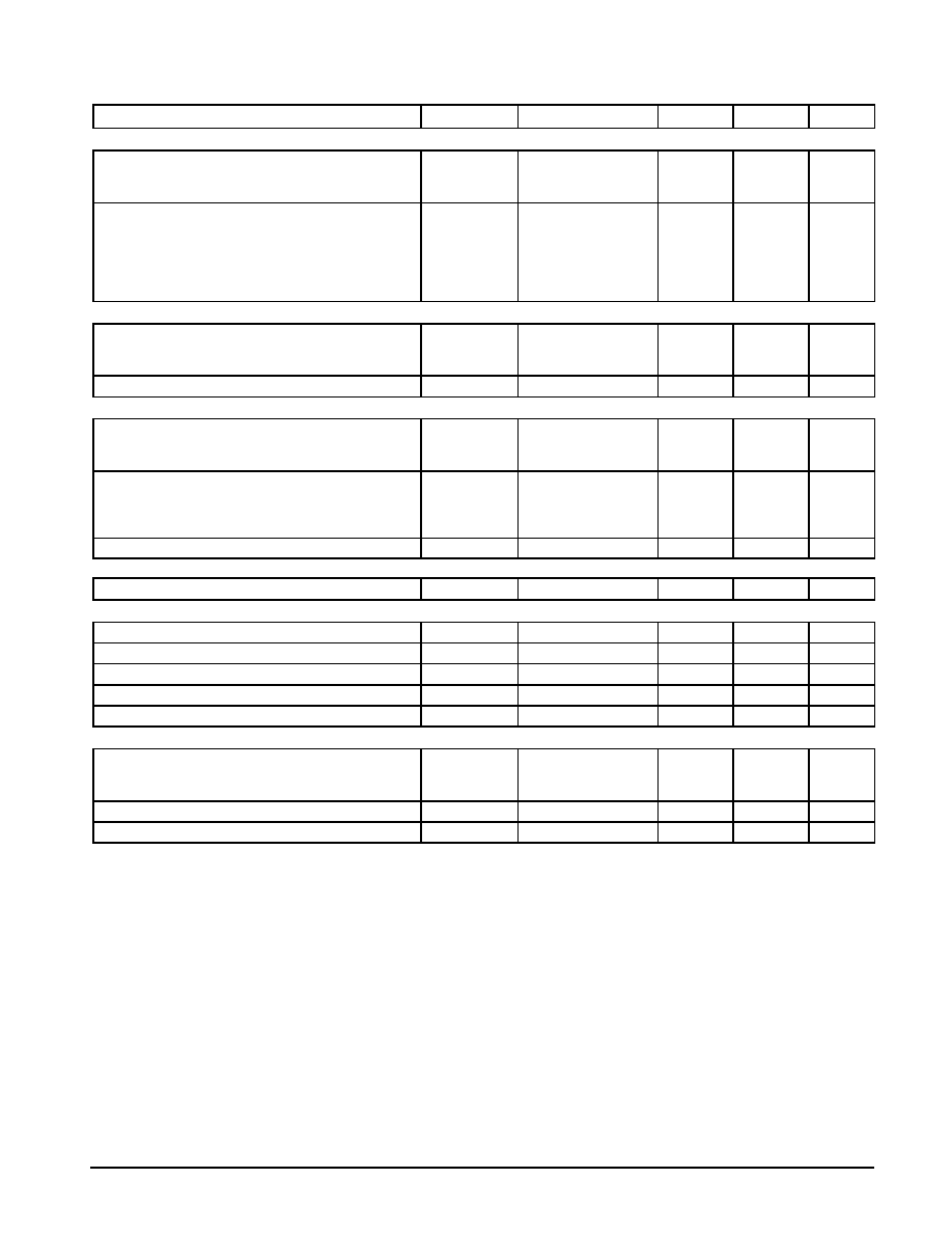
Table 1. Pin Descriptions
4
. . . . . . . . . . . . . . . . . . . . . . . . . . . . . . . . . . . . . . . . . . . . . . . . . . . . . . . . . . . . . . . . . . . . . . . . . . . . . . . . . .
Controller Interface Pins
4
. . . . . . . . . . . . . . . . . . . . . . . . . . . . . . . . . . . . . . . . . . . . . . . . . . . . . . . . . . . . . . . . . . . . . . . . . . . . . . . . . . . . .
AUI Interface Pins
4
. . . . . . . . . . . . . . . . . . . . . . . . . . . . . . . . . . . . . . . . . . . . . . . . . . . . . . . . . . . . . . . . . . . . . . . . . . . . . . . . . . . . . . . . . . .
Twisted Pair Interface Pins
4
. . . . . . . . . . . . . . . . . . . . . . . . . . . . . . . . . . . . . . . . . . . . . . . . . . . . . . . . . . . . . . . . . . . . . . . . . . . . . . . . . . .
Oscillator and Frequency Multiplier Pins
5
. . . . . . . . . . . . . . . . . . . . . . . . . . . . . . . . . . . . . . . . . . . . . . . . . . . . . . . . . . . . . . . . . . . . . . . .
Mode Select Pins
5
. . . . . . . . . . . . . . . . . . . . . . . . . . . . . . . . . . . . . . . . . . . . . . . . . . . . . . . . . . . . . . . . . . . . . . . . . . . . . . . . . . . . . . . . . . .
Status Indicator Pins
6
. . . . . . . . . . . . . . . . . . . . . . . . . . . . . . . . . . . . . . . . . . . . . . . . . . . . . . . . . . . . . . . . . . . . . . . . . . . . . . . . . . . . . . . .
Power Supply and Ground Pins
6
. . . . . . . . . . . . . . . . . . . . . . . . . . . . . . . . . . . . . . . . . . . . . . . . . . . . . . . . . . . . . . . . . . . . . . . . . . . . . . .
Table 2. Controller Interface Selection
7
. . . . . . . . . . . . . . . . . . . . . . . . . . . . . . . . . . . . . . . . . . . . . . . . . . . . . . . . . . . . . . . . . . . . .
Table 3. Controller Independent Mode Selection
7
. . . . . . . . . . . . . . . . . . . . . . . . . . . . . . . . . . . . . . . . . . . . . . . . . . . . . . . . . .
Electrical Characteristics
8
. . . . . . . . . . . . . . . . . . . . . . . . . . . . . . . . . . . . . . . . . . . . . . . . . . . . . . . . . . . . . . . . . . . . . . . . . . . . . . . . . .
Maximum Ratings
8
. . . . . . . . . . . . . . . . . . . . . . . . . . . . . . . . . . . . . . . . . . . . . . . . . . . . . . . . . . . . . . . . . . . . . . . . . . . . . . . . . . . . . . . . . . .
Recommended Operating Conditions
8
. . . . . . . . . . . . . . . . . . . . . . . . . . . . . . . . . . . . . . . . . . . . . . . . . . . . . . . . . . . . . . . . . . . . . . . . . .
ESD
8
. . . . . . . . . . . . . . . . . . . . . . . . . . . . . . . . . . . . . . . . . . . . . . . . . . . . . . . . . . . . . . . . . . . . . . . . . . . . . . . . . . . . . . . . . . . . . . . . . . . . . . .
DC Characteristics
8
. . . . . . . . . . . . . . . . . . . . . . . . . . . . . . . . . . . . . . . . . . . . . . . . . . . . . . . . . . . . . . . . . . . . . . . . . . . . . . . . . . . . . . . .
Power Supply DC Characteristics
8
. . . . . . . . . . . . . . . . . . . . . . . . . . . . . . . . . . . . . . . . . . . . . . . . . . . . . . . . . . . . . . . . . . . . . . . . . . . . .
TTL/CMOS Input and Output DC Characteristics
9
. . . . . . . . . . . . . . . . . . . . . . . . . . . . . . . . . . . . . . . . . . . . . . . . . . . . . . . . . . . . . . . .
Twisted Pair Input and Output DC Characteristics
9
. . . . . . . . . . . . . . . . . . . . . . . . . . . . . . . . . . . . . . . . . . . . . . . . . . . . . . . . . . . . . . .
AUI Input and Output DC Characteristics
10
. . . . . . . . . . . . . . . . . . . . . . . . . . . . . . . . . . . . . . . . . . . . . . . . . . . . . . . . . . . . . . . . . . . . . .
AC Characteristics
12
. . . . . . . . . . . . . . . . . . . . . . . . . . . . . . . . . . . . . . . . . . . . . . . . . . . . . . . . . . . . . . . . . . . . . . . . . . . . . . . . . . . . . . .
External Clock Input (X1) Switching Characteristics
12
. . . . . . . . . . . . . . . . . . . . . . . . . . . . . . . . . . . . . . . . . . . . . . . . . . . . . . . . . . . . .
Receive Phase Locked Loop Switching Characteristics
12
. . . . . . . . . . . . . . . . . . . . . . . . . . . . . . . . . . . . . . . . . . . . . . . . . . . . . . . . . .
Controller Transmit Switching Characteristics (Motorola Mode)
12
. . . . . . . . . . . . . . . . . . . . . . . . . . . . . . . . . . . . . . . . . . . . . . . . . . .
Controller Receive Switching Characteristics (Motorola Mode)
12
. . . . . . . . . . . . . . . . . . . . . . . . . . . . . . . . . . . . . . . . . . . . . . . . . . . .
Controller Transmit Switching Characteristics (Intel Mode)
14
. . . . . . . . . . . . . . . . . . . . . . . . . . . . . . . . . . . . . . . . . . . . . . . . . . . . . . .
Controller Receive Switching Characteristics (Intel Mode)
14
. . . . . . . . . . . . . . . . . . . . . . . . . . . . . . . . . . . . . . . . . . . . . . . . . . . . . . . .
Controller Transmit Switching Characteristics (Fujitsu Mode)
15
. . . . . . . . . . . . . . . . . . . . . . . . . . . . . . . . . . . . . . . . . . . . . . . . . . . . .
Controller Receive Switching Characteristics (Fujitsu Mode)
15
. . . . . . . . . . . . . . . . . . . . . . . . . . . . . . . . . . . . . . . . . . . . . . . . . . . . .
Controller Transmit Switching Characteristics (National Mode)
16
. . . . . . . . . . . . . . . . . . . . . . . . . . . . . . . . . . . . . . . . . . . . . . . . . . . .
Controller Receive Switching Characteristics (National Mode)
16
. . . . . . . . . . . . . . . . . . . . . . . . . . . . . . . . . . . . . . . . . . . . . . . . . . . .
TP Transmit Switching Characteristics
18
. . . . . . . . . . . . . . . . . . . . . . . . . . . . . . . . . . . . . . . . . . . . . . . . . . . . . . . . . . . . . . . . . . . . . . . .
TP Transmit Jabber Switching Characteristics
20
. . . . . . . . . . . . . . . . . . . . . . . . . . . . . . . . . . . . . . . . . . . . . . . . . . . . . . . . . . . . . . . . . .
TP Transmit Signal Quality Error Test Switching Characteristics
20
. . . . . . . . . . . . . . . . . . . . . . . . . . . . . . . . . . . . . . . . . . . . . . . . . .
TP Receive Switching Characteristics
21
. . . . . . . . . . . . . . . . . . . . . . . . . . . . . . . . . . . . . . . . . . . . . . . . . . . . . . . . . . . . . . . . . . . . . . . . .
TP Receive Link Integrity Switching Characteristics
21
. . . . . . . . . . . . . . . . . . . . . . . . . . . . . . . . . . . . . . . . . . . . . . . . . . . . . . . . . . . . .
TP Collision Switching Characteristics
23
. . . . . . . . . . . . . . . . . . . . . . . . . . . . . . . . . . . . . . . . . . . . . . . . . . . . . . . . . . . . . . . . . . . . . . . .
TP Full Duplex Switching Characteristics
23
. . . . . . . . . . . . . . . . . . . . . . . . . . . . . . . . . . . . . . . . . . . . . . . . . . . . . . . . . . . . . . . . . . . . . .
AUI Transmit Switching Characteristics
24
. . . . . . . . . . . . . . . . . . . . . . . . . . . . . . . . . . . . . . . . . . . . . . . . . . . . . . . . . . . . . . . . . . . . . . .
AUI Receive Switching Characteristics
24
. . . . . . . . . . . . . . . . . . . . . . . . . . . . . . . . . . . . . . . . . . . . . . . . . . . . . . . . . . . . . . . . . . . . . . . .
Functional Description
25
. . . . . . . . . . . . . . . . . . . . . . . . . . . . . . . . . . . . . . . . . . . . . . . . . . . . . . . . . . . . . . . . . . . . . . . . . . . . . . . . . . .
Data Transmission
25
. . . . . . . . . . . . . . . . . . . . . . . . . . . . . . . . . . . . . . . . . . . . . . . . . . . . . . . . . . . . . . . . . . . . . . . . . . . . . . . . . . . . . . . . .
Data Reception
26
. . . . . . . . . . . . . . . . . . . . . . . . . . . . . . . . . . . . . . . . . . . . . . . . . . . . . . . . . . . . . . . . . . . . . . . . . . . . . . . . . . . . . . . . . . . .
Collision
26
. . . . . . . . . . . . . . . . . . . . . . . . . . . . . . . . . . . . . . . . . . . . . . . . . . . . . . . . . . . . . . . . . . . . . . . . . . . . . . . . . . . . . . . . . . . . . . . . . .
Jabber
26
. . . . . . . . . . . . . . . . . . . . . . . . . . . . . . . . . . . . . . . . . . . . . . . . . . . . . . . . . . . . . . . . . . . . . . . . . . . . . . . . . . . . . . . . . . . . . . . . . . . .
Full Duplex
26
. . . . . . . . . . . . . . . . . . . . . . . . . . . . . . . . . . . . . . . . . . . . . . . . . . . . . . . . . . . . . . . . . . . . . . . . . . . . . . . . . . . . . . . . . . . . . . . .
Auto Port Selection
26
. . . . . . . . . . . . . . . . . . . . . . . . . . . . . . . . . . . . . . . . . . . . . . . . . . . . . . . . . . . . . . . . . . . . . . . . . . . . . . . . . . . . . . . . .
Auto Polarity Selection
26
. . . . . . . . . . . . . . . . . . . . . . . . . . . . . . . . . . . . . . . . . . . . . . . . . . . . . . . . . . . . . . . . . . . . . . . . . . . . . . . . . . . . . .
Loop Back Mode
26
. . . . . . . . . . . . . . . . . . . . . . . . . . . . . . . . . . . . . . . . . . . . . . . . . . . . . . . . . . . . . . . . . . . . . . . . . . . . . . . . . . . . . . . . . . .
Applications
27
. . . . . . . . . . . . . . . . . . . . . . . . . . . . . . . . . . . . . . . . . . . . . . . . . . . . . . . . . . . . . . . . . . . . . . . . . . . . . . . . . . . . . . . . . . . . . .
Selection of Crystal and External Components
27
. . . . . . . . . . . . . . . . . . . . . . . . . . . . . . . . . . . . . . . . . . . . . . . . . . . . . . . . . . . . . . . . .
PLL Filter Components
27
. . . . . . . . . . . . . . . . . . . . . . . . . . . . . . . . . . . . . . . . . . . . . . . . . . . . . . . . . . . . . . . . . . . . . . . . . . . . . . . . . . . . .
10BASE≠T Filter and Transformer Choice
27
. . . . . . . . . . . . . . . . . . . . . . . . . . . . . . . . . . . . . . . . . . . . . . . . . . . . . . . . . . . . . . . . . . . . .
AUI Transformer Choice
27
. . . . . . . . . . . . . . . . . . . . . . . . . . . . . . . . . . . . . . . . . . . . . . . . . . . . . . . . . . . . . . . . . . . . . . . . . . . . . . . . . . . .

MC68160A
4
MOTOROLA ANALOG IC DEVICE DATA
Table 1. Pin Function Descriptiont
Pin(s)
Symbol
Type
Name/Function
CONTROLLER INTERFACE
1
RENA
O
TTL/CMO
Receive Enable Output: Indication of the presence of network activity, synchronous to
RCLK. In the standby mode, RENA is driven to the high impedance state.
2
RX
O
TTL/CMOS
Receive Data Output: Recovered data, synchronous to RCLK. Following a reset operation,
100 ms should be allowed before attempting to read data processed by the MC68160A, B
and C. This delay is needed to insure that the receive phase locked loop is properly
synchronized with incoming data. In the standby mode, RX is driven to the high impedance
state.
48
TCLK
O
TTL/CMOS
Transmit Clock Output CMOS/TTL Output: TCLK provides a symmetrical clock signal at
10 MHz for reference timing of data to be encoded. In the standby mode, TCLK is driven to
the high impedance state.
49
TENA
I
TTL
Transmit Enable Input: Input signal synchronous to TCLK which enables data transmission
on the active port. An internal pull≠down resistor is provided so that the input is low under no
connect conditions. (This resistor is removed in the standby mode). If TENA is asserted at
the conclusion of a reset operation, it must first be deasserted and then reasserted before
data transmission can occur. In the standby mode, TENA is driven to the high impedance
state.
50
RCLK
O
TTL/CMOS
Receive Clock Output: Recovered clock. In the standby mode, RCLK is driven to the high
impedance state.
51
CLSN
O
TTL/CMOS
Collision Output: In the AUI mode, indicates the presence of signals at the ACX+ and
ACX≠ terminals which meet threshold and pulse width requirements. In the TP mode,
indicates simultaneous transmit and receive activity, a heartbeat (SQE Test) signal was
generated, or the jabber timer has expired. In the standby mode, CLSN is driven to the high
impedance state.
52
TX
I
TTL
Transmit Data Input: Input signal synchronous to TCLK which provides NRZ serial data to
be Manchester encoded. In the standby mode, TX is driven to the high impedance state.
AUI INTERFACE
21
22
ACX≠
ACX+
I
AUI Differential Collision Inputs: These inputs are connected to a pair of internally biased
line receivers consisting of a carrier detect receiver with offset threshold and noise filtering to
detect the line activity. Signals at ACX+/≠ have no effect on data path functions.
23
24
ARX≠
ARX+
I
AUI Differential Receiver Inputs: These inputs are connected to a pair of internally biased
line receivers consisting of a carrier detect receiver with offset threshold and noise filtering to
detect the line activity, and a data receiver with no offset for Manchester Data reception.
25
26
ATX≠
ATX+
O
AUI Differential Transmit Outputs : This line pair is intended to operate into terminated
transmission lines. For TX signals meeting setup and hold time to TCLK when TENA is
previously asserted, Manchester encoded data is outputted at ATX+/≠. When operating into a
78
terminated transmission line, signaling meets the required output levels and skew for
IEEE≠802.3 drop cables. When the 10BASE≠T port is automatically or manually selected,
the AUI outputs are driven to a low power standby state in which the outputs deliver a
balanced high state voltage.
TWISTED PAIR INTERFACE
31
32
TPRX≠
TPRX+
I
Twisted Pair Differential Receiver Inputs: These inputs are connected to a receiver with
Smart Squelch capability which only allows differential receive data to pass as long as the
input amplitude is greater than a minimum signal threshold level and a specific pulse
sequence is received. This assures a good signal to noise ratio while the signal pair is active
by preventing crosstalk and impulse noise conditions from activating the receive function.
36
37
TPTX≠
TPTX+
O
Twisted Pair Differential Transmitter Outputs: These lines have pre≠distortion drive
capability and are intended to drive terminated twisted pair transmission lines. When the AUI
port is manually selected, the 10BASE≠T outputs are driven to a low power standby state in
which the outputs deliver a balanced high state voltage. However, when the AUI port is
automatically selected, the 10BASE≠T outputs remain active.
NOTE:
The sense of the controller interface pins will change, depending on the controller selected.
MC68160A
5
MOTOROLA ANALOG IC DEVICE DATA
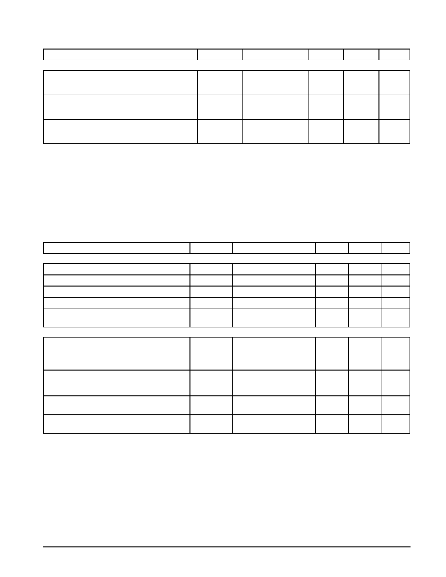
Table 1. Pin Function Description (continued)
Pin(s)
Symbol
Type
Name/Function
OSCILLATOR AND FREQUENCY MULTIPLIER
12
MFILT
C
Frequency Multiplier Filter Connection Point: An external resistor capacitor filter must be
attached to this pin.
16
X1
I/C
CMOS
Oscillator Inverter Input and Crystal Connection Point: When connected for crystal
oscillator operation, the frequency of the clock which appears at TCLK is half that of the
crystal oscillator. As an option, instead of connecting to a crystal, X1 may be driven from an
external 20 MHz CMOS compatible clock generator.
17
X2
O/C
CMOS
Oscillator Inverter Output and Crystal Connection Point: This pin is used only for the
connection of an external crystal and capacitor. It must be left unconnected if X1 is driven by
an external CMOS Clock generator.
MODE SELECT
3
4
5
CS0
CS1
CS2
I
TTL
Mode Select: The logic states applied to these pins select the appropriate interface for the
desired IEEE≠802.3 controller or enable the standby mode. When the standby mode is
selected, the MC68160A power supply current is greatly reduced. Additionally, in the standby
mode, all of the controller inputs and outputs are driven to the high impedance state.
6
LOOP
I
TTL
Diagnostic Loopback: Asserting this function causes serial NRZ data at the TX input to be
Manchester encoded and then looped back through the Manchester decoder, appearing at
the RX output. This diagnostic loopback function operates independent of Twisted Pair (TP)
or Access Unit Interface (AUI) port connectivity or activity. Neither the TP port nor the AUI
port transmits data from the controller while diagnostic loopback is selected. Likewise, the
controller interface receives data neither from the TP nor the AUI receivers while in this
mode. The polarity fault detection and link integrity functions are not inhibited by the
diagnostic loopback mode. If otherwise enabled, they continue to function. If the twisted pair
port is selected, and TPSQEL is driven to the low logic state, a collision detect pulse is
delivered following each transmission to simulate the twisted pair SQE test.
9
APORT
I
TTL
Automatic Port Selection Enable: When high, MC68160A will automatically select the TP
or AUI port based on the presence or absence of valid link beats or frames at the TP receive
input. If the AUI port is automatically selected, the MC68160A will continue to produce link
pulses for the TP port. Changing ports requires approximately 1.0 ms to allow the circuitry for
the new port to resume normal operation. The power consumption is minimized in the
circuitry associated with the unselected port.
27
TPSQEL
I
TTL
Twisted Pair Signal Quality Error Test Enable: Forcing this pin low enables testing of the
internal TP collision detect circuitry after each transmit operation to the TP media. This
function provides a simulated collision to as much of the MC68160A collision detect circuitry
as possible without affecting the attached twisted pair channel. A normal SQE test results in
a high logic state at the CLSN controller interface pin which begins 6 to 16≠bit times after the
last transition of a transmitted signal and continues for 5 to 15≠bit times. (When the AUI port
is selected, SQE test signals are generated by the coaxial cable transceiver and delivered to
the controller via the MC68160A ACX+/≠ receive inputs)
28
TPFULDL
I
TTL
Twisted Pair Full Duplex Mode Select: Forcing this pin low allows simultaneous transmit
and receive operation on the twisted pair port without an indicated collision. This pin is not to
be asserted with LOOP as a test mode is enabled that disrupts normal operation.
29
TPAPCE
I
TTL
Twisted Pair Automatic Polarity Correction Enable: When TPAPCE is high, automatic
polarity correction is enabled, and MC68160A will internally correct for a polarity fault on the
receive circuit. Additionally, when TPAPCE is high, the presence of a polarity fault is
indicated on TPPLR.
46
TPEN
I/O
TTL
(TTL/CMOS)
Twisted Pair Port Enable: If APORT is low, TPEN is an input which determines whether the
AUI port (TPEN low) or TP port (TPEN high) will be manually selected. If the AUI port is
manually selected, the MC68160A will not produce link pulses for the TP port.
If APORT is high, TPEN is an output which will indicate which port has been automatically
selected by driving TPEN low (for AUI) or high (for TP). In its output mode TPEN can sink
10 mA in the low output state and source 10 mA in the high output state. (See Pin 9
Description.)
Changing ports requires approximately 1.0 ms to allow the circuitry for the new port to
resume normal operation. The power consumption is minimized in the circuitry associated
with the unselected port. In the standby mode, this pin is driven to the high impedance state.
MC68160A
6
MOTOROLA ANALOG IC DEVICE DATA
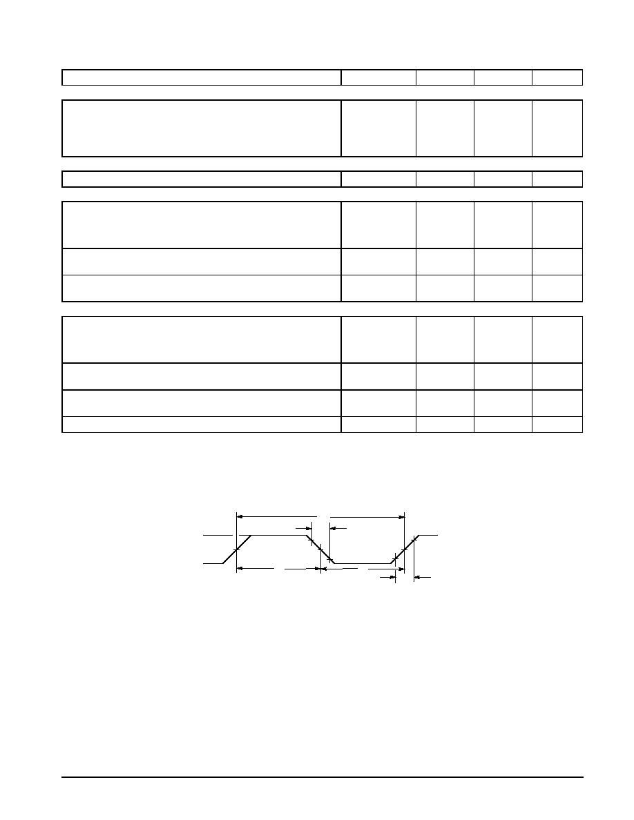
Table 1. Pin Function Description (continued)
Pin(s)
Symbol
Type
Name/Function
STATUS INDICATOR
40
TXLED
O
TTL/CMOS
Transmit Status LED Driver Output: This pin indicates the transmit status of the currently
selected TP or AUI port. When there is no transmit activity detected, an internal pull≠up takes
this pin to its normal off (high) state. When transmit activity is detected, the LED driver turns
on. In its on state, TXLED flashes the LED by driving low at approximately 10 Hz at a 50%
duty cycle. In the standby mode, this output is driven to the high impedance state.
41
RXLED
O
TTL/CMOS
Receive Status LED Driver Output: This pin indicates the receive status of the currently
selected TP or AUI port. When there is no receive activity detected, an internal pull≠up takes
this pin to its normal off (high) state. When receive activity is detected, the LED driver turns
on. In its on state, RXLED flashes the LED by driving low at approximately 10 Hz at a 50%
duty cycle. In the standby mode, this output is driven to the high impedance state.
42
CLLED
O
TTL/CMOS
Collision Status LED Driver Output: This pin indicates the collision status of the currently
selected TP or AUI port. When there is no collision activity detected, an internal pull≠up takes
this pin to its normal off (high) state. When collision activity is detected, the LED driver turns
on. In its on state, CLLED flashes the LED by driving low at approximately 10 Hz at a 50%
duty cycle. In the standby mode, this output is driven to the high impedance state.
43
TPLIL
O
TTL/CMOS
Twisted Pair Link Integrity Output: This output is driven to the low output state to indicate
good link integrity on the TP port during TP mode. It is deasserted (high) when link integrity
fails in TP mode. The TPLIL output is driven to the high impedance state when the AUI port
is selected. In the standby mode, this output is also driven to the high impedance state.
44
TPPLR
O
TTL/CMOS
Twisted Pair Polarity Error Output: If TPAPCE is high and the wires connected to the
Twisted Pair Receiver Inputs (TPRX+, TPRX≠) are reversed, TPPLR will be driven to the low
logic state to indicate the fault. TPPLR remains low when the MC68160A, AB and AC has
automatically corrected for the reversed wires. If the twisted pair link integrity tests fail, this
output will be driven to the high logic state. When the AUI mode is selected this output is
driven to the high impedance state. In the standby mode, this output is also driven to the high
impedance state.
45
TPJABB
O
TTL/CMOS
Twisted Pair Jabber Output: This pin is driven high to indicate a jabber condition at the
TPTX+/≠ outputs. (Jabber condition also causes CLLED to be driven alternately to the high
and low output levels). TPJABB is driven to the low output state when no jabber condition is
present. When the AUI mode is selected this output is driven to the high impedance state. In
the standby mode, this output is also driven to the high impedance state.
POWER SUPPLY AND GROUND
10
VDDDIV
Frequency Divider Supply Pin
11
13
VDDFM
GNDFM
Frequency Multiplier Supply and Ground Pins
14
15
GNDVCO
VDDVCO
Voltage Controlled Oscillator Ground and Supply Pins
20
GNDSUB
Substrate Ground Pin
7
8
18
19
VDDDIG
GNDDIG
VDDDIG
GNDDIG
Digital Supply and Ground Pins
30
33
VDDANA
GNDANA
Analog Supply and Ground Pins
34
35
38
39
GNDPWR
VDDPWR
VDDPWR
GNDPWR
Power Supply and Ground Pins
47
GNDCTL
Controller Interface Ground Pin
NOTE:
Power and ground pins are not connected internally. Failure to connect externally may cause malfunction or damage to the IC.
MC68160A
7
MOTOROLA ANALOG IC DEVICE DATA
Table 2. Controller Interface Selection
Motorola
Transceiver
MC68160A
(EEST
TM
)
Motorola
Controller2
MC68360
(QUICC
TM
)
Intel4
Controllers
82586, 82590,
82593, 82596
Fujitsu4
Controllers
86950 (Etherstar
TM
)
86960 (NICE
TM
)
National4
Controllers
8390, 83C690,
83932B (SONIC
TM
)
CS0
CS1
CS2
1
1
0
0
1
0
1
0
0
0
0
0
Pin
Pin
Sense
Pin
Sense
Pin
Sense
Pin
Sense
TCLK
TCLK
High
TXC
Low
TCKN
Low
TXC
High
TX
TX
High
TXD
High
TXD
High
TXD
High
TENA
TENA
High
RTS
Low
TEN
High
TXE
High
RCLK
RCLK
High
RXC
Low
RCN
Low
RXC
High
RX
RX
High
RXD
High
RXD
High
RXD
High
RENA
RENA
High
CRS
Low
XCD
High
CRS
High
CLSN
CLSN
High
CDT
Low
XCOL
Low
COL
High
LOOP1
N.A.
High
LPBK
Low
LBC
High
LPBK
High
NOTES: 1. Although LOOP input is not ordinarily classifed as a controller pin, it is included in this table because its sense varies according to the controller used.
2. The Motorola controller interface contained in the MC68360 (QUICC
TM
) is compatible with the AMD 7990 (LANCE
TM
) and 79C900 (ILACC
TM
) controllers.
3. The pin sense is shown from the perspective of the identified controller pin.
4. Supported only by MC68160A.
Table 3. Controller Independent Mode Selection
Pin
Standby Mode
Reserved
Reserved
Reserved
CS0
CS1
CS2
1
1
1
0
1
1
1
0
1
0
0
1
NOTE: In standby mode, the MC68160A consumes less power supply current than in any other
mode. Additionally, in the standby mode, all of the controller inputs and outputs are
driven to the high impedance state. When the standby mode is deasserted, an internal
reset pulse of approximately 6.0
µ
s duration is generated.
Following a period of operation in the standby mode, the time required to insure stable
data reception is approximately 100 ms.
TPTX+
TPTX≠
TPRX+
TPRX≠
ATX+
ACX≠
ACX+
ATX≠
ARX+
ARX≠
TCLK
TX
TENA
RCLK
RX
RENA
CLSN
TPTX+
TPRX+
TPRX≠
TPTX≠
ACX≠
ACX+
ARX≠
ARX+
ATX≠
ATX+
Figure 2. Applications Block Diagram
Pulse
Transformers
DB≠15
Connector
Filters
and
Pulse
Transformers
RJ≠45
Connector
LAN
Controller
MC68160A

MC68160A
8
MOTOROLA ANALOG IC DEVICE DATA
ELECTRICAL CHARACTERISTICS
MAXIMUM RATINGS
Characteristic
Symbol
Min
Max
Unit
Storage Temperature Range
Tstg
≠ 65
150
∞
C
Power Supply Voltage Range
Analog
Digital
VDDA
VDDD
≠
≠
7.0
7.0
V
Voltage on any TTL compatible input pin with
respect to Ground
Voltage on TPRX, ARX, or ACX input pins with
respect to Ground
V
≠ 0.5
≠ 0.5
VDD + 0.5
6.0
V
Differential Voltage on TPRX, ARX, or ACX Input
Pins
VDIFF
≠ 6.0
6.0
V
NOTE:
Stresses in excess of the Absolute Maximum Ratings can cause permanent damage to the
device. Functional operation of the device is not implied at these or any other conditions in
excess of those indicated in the operation sections of this data sheet. Exposure to Absolute
Maximum Ratings conditions for extended periods can adversely affect device reliability.
RECOMMENDED OPERATING CONDITIONS
Characteristic
Symbol
Min
Max
Unit
Power Supply Voltage Range
VDD
4.75
5.25
V
Power Supply Ripple (20 kHz to 100 kHz)
≠
≠
50
mV
Power Supply Impulse Noise (Either Polarity)
≠
≠
100
mV
Ambient Operating Temperature Range
TA
0
70
∞
C
ARX/ACX Input Differential Rise and Fall Time (see Figure 39)
t260
2.0
10
ns
ARX Pair Idle Time after Transmission (see Figure 39)
t265
8.0
≠
µ
s
ESD
Although protection circuitry has been designed into this device, proper precautions should be taken to avoid exposure to electrostatic discharge
(ESD) during handling and mounting. Motorola employs a Human Body Model (HBM) and a Charged Device Model (CDM) for ESD≠susceptibility
testing and protection design evaluation. ESD has been adopted for the CDM, however, a standard HBM (resistance = 1500
capacitance ≠
100 pF) is widely used and, therefore, can be used for comparison purposes. The HBM ESD threshold presented here was obtained by using
the circuit parameters contained in this specification. ESD threshold voltage is designed to 700 V Human Body Model.
DC ELECTRICAL CHARACTERISTICS
(Unless otherwise noted, minimum and maximum limits apply over the recommended
ambient operating temperature and power supply voltage ranges.)
Characteristic
Symbol
Test Conditions
Min
Typ
Max
Unit
POWER SUPPLY
Undervoltage Shutdown Threshold
≠
≠
≠
≠
4.4
V
Power Supply Current
IDD
≠
Standby Mode
≠
≠
145
≠
200
5.0
mA
MC68160A
9
MOTOROLA ANALOG IC DEVICE DATA
DC ELECTRICAL CHARACTERISTICS
(TA = 25
∞
C, VCC = 5.0 V
±
5%. Unless otherwise noted, minimum and maximum
limits apply over the recommended ambient operating temperature and power supply voltage ranges for each MC68160A except where noted.)
Characteristic
Symbol
Test Conditions
Min
Max
Unit
TTL COMPATIBLE INPUTS
TTL Compatible Input Voltage
Low State
High State
VIL(TTL)
VIH(TTL)
≠
≠
2.0
0.8
≠
V
Input Current TTL Compatible Input Pins (Note 1)
Input Current TENA TTL Compatible Input Pin:
with Pull≠Down Resistor
IIH
IIL
with Pull≠Down Resistor removed in Standby Mode
IIH
IIL
IIH & IIL
0 V < VI < VDD
≠
≠
≠
≠
±
10
+200
≠ 20
±
10
µ
A
CMOS COMPATIBLE INPUTS
CMOS Compatible Input Voltage
Low State
High State
VIL(CMOS)
VIH(CMOS)
≠
≠
3.0
1.0
≠
V
Input Current (Pin X1)
IIH & IIL
0 V < VI < VDD
≠
±
100
µ
A
TTL/CMOS COMPATIBLE OUTPUTS
TTL/CMOS Compatible Output Voltage
Low State (Note 2)
Low State (Note 3)
VOL
IOL = 4.0 mA
IOL = 10 mA
≠
≠
0.45
0.45
V
TTL/CMOS Compatible Output Voltage
High State (Note 4)
High State (Note 5)
High State (Note 2)
VOH
IOH = ≠ 500
µ
A
IOH = ≠ 10 mA
IOH = ≠ 4.0 mA
3.9
3.9
2.4
≠
≠
≠
V
Three State Output Leakage Current
IOZ
0 V
VOZ
VDD
≠
±
10
µ
A
Characteristic
Symbol
Test Conditions
Min
Max
Unit
TWISTED PAIR RECEIVER INPUTS
Input Voltage Range (DC + AC)
VITP
≠
1.5
4.3
V
Differential Input Squelch Threshold Voltage
VITPSQ
Note 10
270
390
mV
Common Mode Bias Generator Voltage
VBCMTP
Note 9
1.8
3.2
V
Common Mode Input Resistance
RCMTP
≠
1000
≠
Differential Input Resistance
RDIFFTP
≠
2.5
≠
k
TWISTED PAIR TRANSMITTER OUTPUTS
Differential Output Voltage
Pre≠Emphasis Level
Signal Level
VODFTPP
VODFTPS
Note 7
±
2.2
±
1.56
±
2.8
±
1.98
V
Common Mode Output Voltage Range
VOCMTP
Note 6
0
4.0
V
Common Mode Output Voltage in Standby Mode
VOCMTPSB
IOH = ≠100
µ
A
VDD ≠ 1.0
VDD
V
NOTES: 1. APORT, TPAPCE, CS0, CS1, CS2, TX, LOOP, TPFULDL, TPSQEL and TPEN (In Input Mode).
2. TCLK, RX, RCLK, RENA and CLSN.
3. TPPLR, TPLIL, TPJABB, TXLED, RXLED, CLLED and TPEN (In Output Mode).
4. TPPLR, TPLIL, CLLED, TXLED and RXLED.
5. TPJABB and TPEN (In Output Mode).
6. Measured with Test Load B1 (shown in Figure 3), applied directly to the TPTX+/≠ pins of the device.
7. Measured differentially with Test Load B2 (shown in Figure 4), applied directly to the TPTX+/≠ pins of the device.
8. Measured directly on the TPTX+/≠ pins of the device.
9. Measured with Test Load B3 (shown in Figure 5), applied directly to the TPRX+/≠ pins of the device.
10. The Common Mode Input Voltage is between 1.8 V and 3.2 V.
MC68160A
10
MOTOROLA ANALOG IC DEVICE DATA
DC ELECTRICAL CHARACTERISTICS
(continued) (TA = 25
∞
C, VCC = 5.0 V
±
5%. Unless otherwise noted, minimum and maximum
limits apply over the recommended ambient operating temperature and power supply voltage ranges for each MC68160A except where noted.)
Characteristic
Symbol
Test Conditions
Min
Max
Unit
TWISTED PAIR TRANSMITTER OUTPUTS
Differential Output Voltage
IDLE Mode
Open Circuit
VODFTPI
VODFTPO
Note 6
Note 8
≠
≠
±
50
5.25
mV
V
Differential Output Impedance
TRANSMISSION Mode
IDLE Mode
RODFTPT
RODFTPI
Note 8
12
8.0
28
29
Common Mode Output Impedance
TRANSMISSION Mode
IDLE Mode
ROCMTPT
ROCMTPI
Note 8
3.0
1.0
7.0
10
NOTES: 1. APORT, TPAPCE, CS0, CS1, CS2, TX, LOOP, TPFULDL, TPSQEL and TPEN (In Input Mode).
2. TCLK, RX, RCLK, RENA and CLSN.
3. TPPLR, TPLIL, TPJABB, TXLED, RXLED, CLLED and TPEN (In Output Mode).
4. TPPLR, TPLIL, CLLED, TXLED and RXLED.
5. TPJABB and TPEN (In Output Mode).
6. Measured with Test Load B1 (shown in Figure 3), applied directly to the TPTX+/≠ pins of the device.
7. Measured differentially with Test Load B2 (shown in Figure 4), applied directly to the TPTX+/≠ pins of the device.
8. Measured directly on the TPTX+/≠ pins of the device.
9. Measured with Test Load B3 (shown in Figure 5), applied directly to the TPRX+/≠ pins of the device.
10. The Common Mode Input Voltage is between 1.8 V and 3.2 V.
DC ELECTRICAL CHARACTERISTICS
(Unless otherwise noted, minimum and maximum limits apply over the recommended
ambient operating temperature and power supply voltage ranges.)
Characteristic
Symbol
Test Conditions
Min
Max
Unit
AUI RECEIVER INPUTS
Input Voltage Range (DC + AC)
VIA
≠
1.0
4.2
V
Differential Mode Input Voltage Range
VIDFA
≠
±
318
±
1315
mV
Differential Input Squelch Threshold Voltage
VIASQ
≠
≠ 275
≠175
mV
Common Mode Input Resistance
RICMA
1.0 V < VICMA < 4.2 V
1.5
≠
k
Differential Input Resistance (ARX, ACX Inputs)
RIDFA
1.0 V < VICMA < 4.2 V
318 mV < VIDMA < 1315 mV
5.0
≠
k
AUI TRANSMITTER OUTPUTS
Common Mode Output Voltage
IDLE Mode
ACTIVE Mode
STANDBY Mode
VOCMIA
VOCMAA
VOCMSA
Figure 6
IO = ≠100
µ
A
1.0
1.0
VDD ≠ 2.0
4.2
4.2
VDD ≠ 1.2
V
Differential Output Voltage
IDLE Mode
ACTIVE Mode
VODFIA
VODFAA
Figure 6
≠
±
600
±
40
±
1315
mV
Differential Output Load Current
IDLE Mode
IODFIA
Figure 7
≠
±
4.0
mA
Output Short Circuit Current
IODSA
Output Short Circuited to
VDD or GND
≠
±
150
mA

MC68160A
11
MOTOROLA ANALOG IC DEVICE DATA
Device
39
39
100
V1
NOTE:
A total of 50
per driver output is required for proper series line termination. This is realized with the
39
external resistors shown in Figures 3, 4 and 5, together with the internal driver output resistance.
Figure 3. Test Load B1
Figure 4. Test Load B2
Figure 5. Test Load B3
+
≠
VCMD
Device
39
39
RCM
1.0 k
+
≠
VCMD
Device
39
39
RCM
10 k
≠
+
Figure 6. AUI Common Mode Termination
VCM
VDIFF
IO
39
39
IOD
Figure 7. AUI Differential Output
Short Circuit Current
MC68160A
12
MOTOROLA ANALOG IC DEVICE DATA
AC ELECTRICAL CHARACTERISTICS
(Unless otherwise noted, minimum and maximum limits apply over the recommended
temperature and power supply voltage ranges.)
Characteristic
Symbol
Min
Max
Unit
EXTERNAL CLOCK INPUT (X1)
Cycle Time (Note 1) (See Figure 8)
Fall Time
Rise Time
Low Time
High Time
t1
t2
t3
t4
t5
49.995
≠
≠
20
20
50.005
5.0
5.0
30
30
ns
RECEIVE PHASE≠LOCKED≠LOOP SWITCHING
Stabilization Time
t7
≠
100
ms
CONTROLLER TRANSMIT SWITCHING (MOTOROLA MODE)
TCLK Cycle Time
TCLK High Time
TCLK Low Time
TCLK Rise and Fall Time
t10
t11
t12
t13
99
45
45
≠
101
55
55
8.0
ns
TX Setup Time to TCLK
TX Hold Time to TCLK
t14
t15
20
0
≠
≠
ns
TENA Setup Time to TCLK
TENA Hold Time to TCLK
t16
t17
20
0
≠
≠
ns
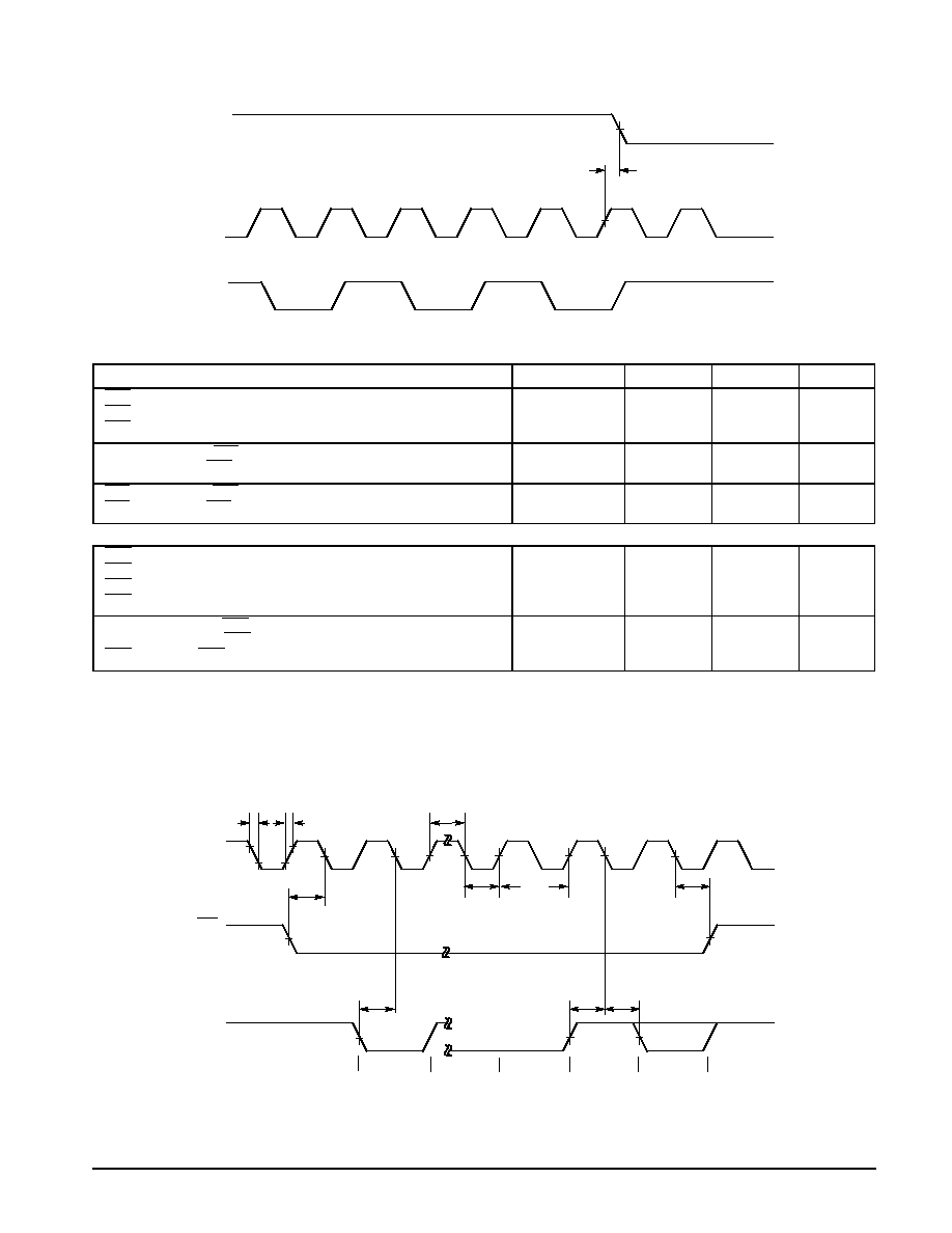
CONTROLLER RECEIVE SWITCHING
RCLK Cycle Time
RCLK High Time
RCLK Low Time
RCLK Rise and Fall Time
t20
t21
t22
t23
90
42
47
≠
≠
≠
55
8.0
ns
RX Hold Time from RCLK
RX Set≠Up Time to RCLK
t24
t24.1
10
70
≠
≠
ns
RCLK Delay from RENA
RX Delay from RENA
t25
t26
≠
≠
650
600
ns
RENA Deassertion Delay from RCLK
(See Figure 12)
t27
10
30
ns
NOTES: 1. To meet IEEE≠802.3 specifications.
2. Load on specified output is 20 pF to ground, unless otherwise noted.
3.
= Rising Edge
t1
4.0V
3.6V
0.4V
0V
3.6V
0.4V
1.5V
1.5V
1.5V
t2
t3
t4
t5
Figure 8. X1 Input Voltage Levels for Timing Measurements
MC68160A
13
MOTOROLA ANALOG IC DEVICE DATA
1.5V
1.5V
Figure 9. Receive Phase≠Locked≠Loop Switching
CS0
D CS1 D CS2
TPRX
RENA
t7
NOTE:
CS0
∑
CS1
∑
CS2 is the logical AND operation and refers to the pins not at Logic 1.
t12
t16
t11
TCLK
TENA
TX
1.5V
1.5V
1.5V
1.5V
3V
0.8V
3V
1.5V
1.5V
1.5V
1.5V
1.5V
1.5V
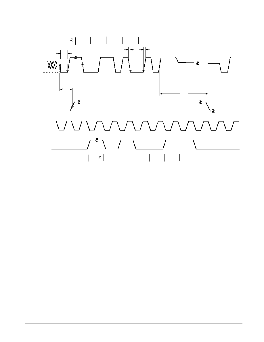
Figure 10. Transmit Timing (Motorola Mode)
t17
t10
t14
t15
t13
t13
t24
RENA
RCLK
RX
1.5V
1.5V
0.8V
3V
0.8V
3V
1.5V
1.5V
1.5V
1.5V
1.5V
1.5V
t25
t26
t20
t22
t21
t23
t23
Figure 11. Receive Timing (Motorola Start of Frame)
t24.1
MC68160A
14
MOTOROLA ANALOG IC DEVICE DATA
t27
RENA
RCLK
Last Bit
1.5V
1.5V
RX
Figure 12. Receive Timing (Motorola End of Frame)
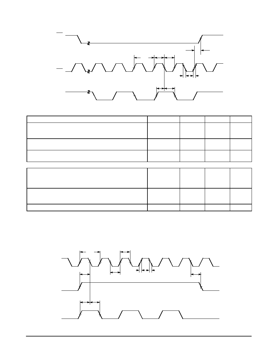
CONTROLLER TRANSMIT SWITCHING (Intel Mode ≠ Support by MC68160A Only)
Characteristic
Symbol
Min
Max
Unit
TXC Cycle Time
TXC High and Low Time
TXC Rise and Fall Time
t40
t41
t42
99
40
≠
101
≠
5.0
ns
TXD Setup Time to TXC
TXD Hold Time to TXC
t43
t44
20
0
≠
≠
ns
RTS Setup Time to TXC
RTS Hold Time to TXC
t45
t46
20
0
≠
≠
ns
CONTROLLER RECEIVE SWITCHING
RXC Cycle Time
RXC High Time
RXC Low Time
RXC Rise and Fall Time
t80
t81
t82
t83
90
45
40
≠
≠
55
≠
5.0
ns
RXD Hold Time from RXC
RXD Set≠Up Time to RXC
CRS Delay from RXC
t85
t85.1
t86
50
35
12
≠
≠
30
ns
NOTE:
Load on specified output is 20 pF to ground, unless otherwise noted.
= Rising Edge
= Falling Edge
t41
t46
t44
t43
t43
t41
t45
t42
t42
TXC
TXD
Last Bit
1
1
0
0
0
1 / 0
1.5V
1.5V
1.5V
1.5V
1.5V
1.5V
0.8V
3V
3V
1.5V
1.5V
1.5V
1.5V
1.5V
Figure 13. Transmit Timing (Intel)
t40
RTS
MC68160A
15
MOTOROLA ANALOG IC DEVICE DATA
t85
t86
t83
t83
t85.1
1.5V
1.5V
1.5V
3V
.8V
3V
1.5V
1.5V
1.5V
1.5V
Figure 14. Receive Timing (Intel)
t80
t81
t82
CRS
RXC
RXD
CONTROLLER TRANSMIT SWITCHING (Fujitsu Mode ≠ Supported by MC68160A Only)
Characteristic
Symbol
Min
Max
Unit
TCKN Cycle Time
TCKN High and Low Time
TCKN Rise and Fall Time
t90
t91
t92
99
45
≠
101
55
8.0
ns
TXD Setup Time to TCKN
TXD Hold Time to TCKN
t93
t94
20
0
≠
≠
ns
TEN Setup Time to TCKN
TEN Hold Time to TCKN
t95
t96
20
0
≠
≠
ns
CONTROLLER RECEIVE SWITCHING
RCKN Cycle Time
RCKN High Time
RCKN Low Time
RCKN Rise and Fall Time
t100
t101
t102
t103
90
40
45
≠
≠
≠
55
8.0
ns
RXD Hold Time from RCKN
RXD Set≠Up Time RCLK
RCKN Delay from XCD
t104
t104.1
t105
50
35
≠
≠
≠
600
ns
XCD Deassertion Delay from RCKN
(See Figure 17)
t106
0
≠
ns
NOTE:
Load on specified output is 20 pF to ground, unless otherwise noted.
= Rising Edge
= Falling Edge
t96
t92
t92
t91
t95
t94
TCKN
TEN
TXD
1.5V
1.5V
1.5V
1.5V
0.8V
3V
1.5V
1.5V
1.5V
1.5V
1.5V
0.8V
Figure 15. Transmit Timing (Fujitsu)
t90
t91
t93
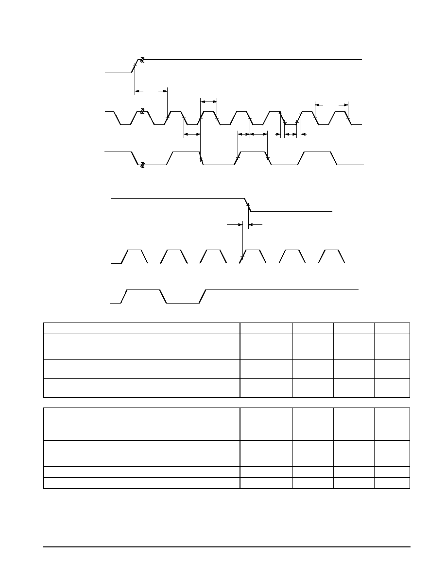
MC68160A
16
MOTOROLA ANALOG IC DEVICE DATA
t104
t104.1
t103
t102
t103
t101
XCD
RCKN
RXD
1.5V
1.5V
3V
0.8V
1.5V
1.5V
1.5V
1.5V
1.5V
1.5V
t105
t100
Figure 16. Receive Timing (Fujitsu Start of Frame)
t106
XCD
RCKN
1.5V
1.5V
RXD
Figure 17. Receive Timing (Fujitsu End of Frame)
CONTROLLER TRANSMIT SWITCHING (National Mode ≠ Supported by MC68160A Only)
Characteristic
Symbol
Min
Max
Unit
TXC Cycle Time
TXC High and Low Time
TXC Rise and Fall Time
t110
t111
t112
99
45
≠
101
55
8.0
ns
TXD Setup Time to TXC
TXD Hold Time to TXC
t113
t114
20
0
≠
≠
ns
TXE Setup Time to TXC
TXE Hold Time to TXC
t115
t116
20
0
≠
≠
ns
CONTROLLER RECEIVE SWITCHING
RXC Cycle Time
RXC Low Time
RXC High Time
RXC Rise and Fall Time
t120
t121
t122
t123
90
40
40
≠
≠
≠
60
8.0
ns
RXD Hold Time from RXC
RXD Set≠Up Time from RXC
RXC Delay from CRS
t124
t124.1
t125
50
35
≠
≠
≠
600
ns
CRS Deassertion Delay from RXC
t126
0
15
ns
RXC continuing beyond CRS
t127
5.0
≠
cycles
NOTE:
Load on specified output is 20 pF to ground, unless otherwise noted.
= Rising Edge
= Falling Edge
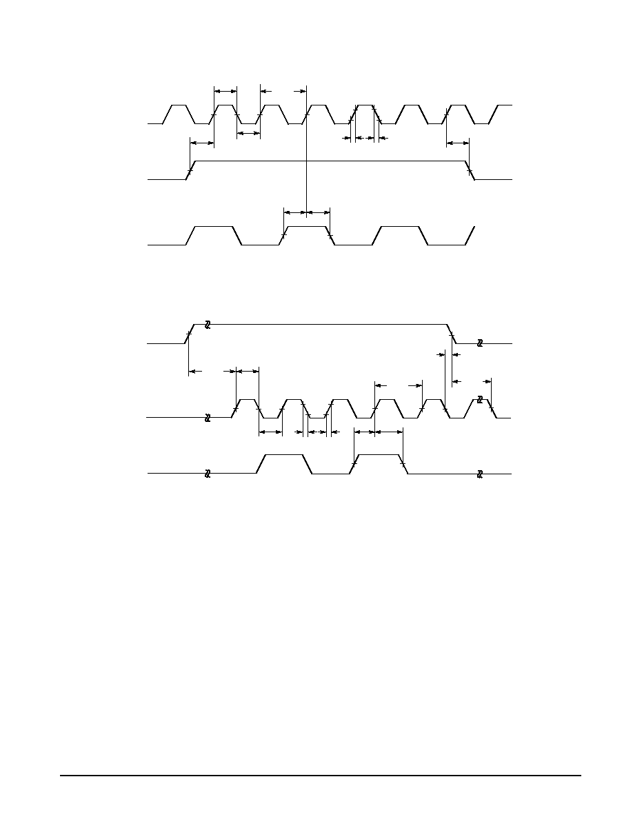
MC68160A
17
MOTOROLA ANALOG IC DEVICE DATA
t113
t114
t116
t112
t115
t111
t111
TXC
TXE
TXD
1.5V
1.5V
1.5V
1.5V
0.8V
3V
0.8V
1.5V
1.5V
1.5V
1.5V
Figure 18. Transmit Timing (National)
t110
t112
t124.1 t124
t126
t121
t123
t123
t122
CRS
RXC
RXD
3V
1.5V
0.8V
1.5V
1.5V
1.5V
1.5V
1.5V
1.5V
1.5V
Figure 19. Receive Timing (National)
t125
t120
t127
MC68160A
18
MOTOROLA ANALOG IC DEVICE DATA
TP TRANSMIT SWITCHING
Characteristic
Symbol
Min
Typ
Max
Unit
TPTX Common Mode AC Output Voltage (Note 3)
VOCMTP
≠
≠
50
mVrms
TX to TPTX Steady State Propagation Delay (Note 2) (See Figure 24)
Bit Duration Center≠to≠Center
Half≠Bit Cell Duration Center≠to≠Boundary
t130
t131
t132
≠
98
48
≠
≠
≠
200
102
52
ns
TENA Assert to RENA Assert Delay (Note 7) (See Figure 24)
t133
≠
≠
400
ns
Internal Loopback Delay from TX to RX (Note 7) (See Figure 24)
t134
≠
≠
650
ns
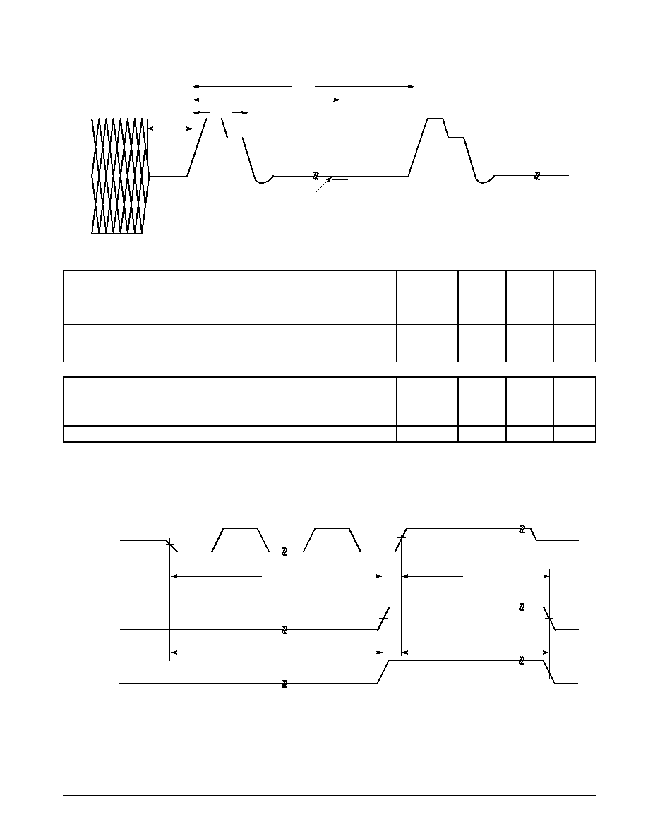
TPTX End of Packet Hold Time from last positive TPTX Signal Edge to
+585 mV Differential Output Level (Note 5) (See Figure 25)
t135
250
≠
400
ns
TPTX Precompensation Pulse Width (Notes 2 and 6) (See Figure 25)
t136
≠
45≠58
≠
ns
RENA Deassert Delay from TENA Deassert when Receiver is inactive
Motorola Mode
Fujitsu Mode
National Mode
Intel Mode (Note 4) (See Figure 26)
t137
t137
t137
t138
250
250
250
250
≠
≠
≠
≠
450
450
450
450
ns
TPTX Data≠to≠Link Test Pulse (Note 2) (See Figure 27)
TPTX Link Test Pulse Width (Note 2)
TPTX Link Test Pulse Decay≠to≠Idle Condition (Note 1)
TPTX Link Test Pulse to next Link Test Pulse (Note 2)
t139
t140
t141
t142
8.0
80
80
8.0
≠
≠
≠
≠
24
240
240
24
ms
ns
ns
ms
NOTES: 1. Measured differentially across the output of Test Load A which is connected directly to the TPTX+/≠ pins of the device.
2. Measured differentially across the output of Test Load D shown in Figure 23 which is connected directly to the TPTX+/≠ pins of the device.
3. Measured across the output of Test Load C which is connected directly to the TPTX+/≠ pins of the device.
4. Same as t137 except the logic states for TENA and RENA are inverted.
5. Measured across the output of Test Load B shown in Figure 21.
6. Measured at the +/≠90% points of the precompensation voltage feature of the waveform. (The 0% reference is 0 V differential.)
7. Load on specified output is 20 pF to ground.
100
µ
H
Device
39
39
1.0
µ
H
1.0
µ
H
100pF
100pF
VOUT
100
39
39
100
200
µ
H
39
39
47.5
47.5
49.9
VCM
200
µ
H
39
39
100
VOUT
NOTE:
A total of 50
per driver output is required for proper series line termination.
This is realized with the 39
external resistors shown in Figures 20 to 23,
together with the internal driver output resistance.
Vout
Figure 20. Test Load A
Figure 21. Test Load B
Figure 22. Test Load C
Figure 23. Test Load D

MC68160A
19
MOTOROLA ANALOG IC DEVICE DATA
t130
t131
t132
1
0
1
X1
TCLK
TENA
TX
0
0
1
1
1
1
1
1
0
0
0
1
0
1
0
0
1
1
RENA
RX
1
1
1
1
0
0
0
1.5V
1.5V
1.5V
1.5V
0V
t133
t134
1.5V
TPTX +/≠ Differential
(Logic Levels)
TPTX +/≠ Differential
(Pre≠Emphasis)
Figure 24. TPTX Transmit Timing (Start of Frame) Switching
t136
90%
90%
+585mV
+585mV
Figure 25. TPTX Transmit Timing (End of Frame) Switching
TPTX +/≠
Differential
t135
1.5V
TENA
RENA
1.5V
Figure 26. RENA Deassert Delay from TENA
t137
MC68160A
20
MOTOROLA ANALOG IC DEVICE DATA
t140
585mV
585mV
585mV
Figure 27. TPTX+/≠ Link Pulse Timing
t142
t141
t139
±
50mV
TP TRANSMIT JABBER SWITCHING
Characteristic
Symbol
Min
Max
Unit
Max Length of Transmission before Assertion
of TPJABB to indicate Jabber Condition
CLSN to indicate Jabber Condition
t160
t161
20
20
60
60
ms
Time from End of Jabber Condition to Deassertion:
of TPJABB
of CLSN
t162
t163
500
500
750
750
ms
TP TRANSMIT SIGNAL QUALITY ERROR TEST SWITCHING
CLSN (Signal Quality Error Test) (See Figure 29)
A
ti
f
l
t
iti
TPTX d
t
0 6
1 6
µ
s
Assertion from last positive TPTX edge
Deassertion from last positive TPTX edge
t170
t171
0.6
≠
1.6
3.1
Deassertion from last ositive TPTX edge
Pulse Width
t171
t172
0.5
3.1
1.5
TPSQEL Disable Delay Time (See Figure 29)
t173
≠
40
ns
NOTE:
The load attached to the specified output is a 20 pF capacitor connected to ground, unless otherwise noted.
TPTX
≠585mV
TPJABB
1.5V
1.5V
(Differential)
585mV
CLSN
1.5V
1.5V
Figure 28. TPJABB Switching
t160
t161
t163
t162

MC68160A
21
MOTOROLA ANALOG IC DEVICE DATA
TPTX+/≠
CLSN
1.5V
2V
1.5V
TPSQEL
1.5V
Figure 29. TPTX SQE (CLSN) Timing (End of Frame)
t173
t171
t170
t172
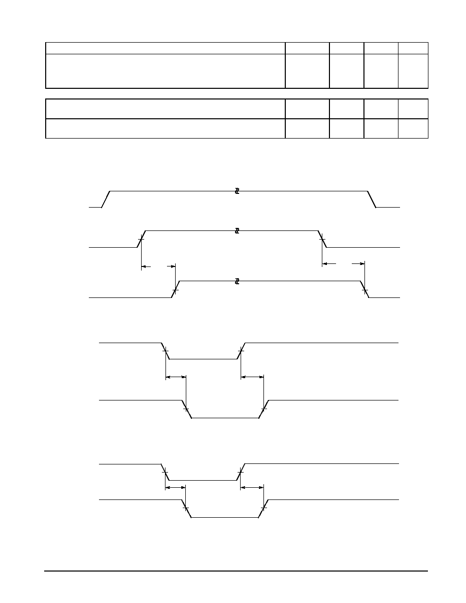
TP RECEIVE SWITCHING
Characteristic
Symbol
Min
Max
Unit
Differential Input Voltage Range Unconditional Squelch (Note 1)
(1.8 V < Input Common Mode Voltage < 3.2 V)
VIDFSTP
0
|264|
mV
Positive or Negative Differential Input Pulse Width for Conditional Receive Unsquelch
(See Figure 31)
t180
20
30
ns
TPRX to RCLK Bit Loss at start of packet (See Figure 32)
t181
≠
10
Bits
TPRX to RCLK Steady State Propagation Delay (See Figure 32)
t182
≠
400
ns
TPRX to RX Start Up Delay (See Figure 32)
t183
≠
1.5
µ
s
TPRX held high from last valid positive transition (See Figure 33)
t186
230
≠
ns
RENA Deassertion Delay from last valid positive transition of TPRX Pair
(See Figure 33)
t187
≠
350
ns
TP RECEIVE LINK INTEGRITY SWITCHING
Required Pulse Width Range to be recognized as a Link Pulse (Note 2)
t200
50
200
ns
Last TPRX activity to high state TPLIL Output
(Receive Link Loss Timeout Interval)
t201
100
150
ms
Receive Link Beat Separation
Minimum Range (Note 3)
Maximum Range (Note 4)
t202
t203
3.0
100
7.0
150
ms
NOTES: 1. Measured with Test Load H attached to the receive pins.
2. Measured at the receive pins.
3. Link beats closer in time to this range of values are considered noise, and are rejected.
4. Link beats further apart in time than this range of values are not considered consecutive, and are rejected.
t180
t180
TPRX
≠330mV
+330mV
0mV
200
µ
H
100
1.0
µ
H
1.0
µ
H
100pF
100pF
Line
Figure 30. Test Load H
Figure 31. TPRX Input Switching

MC68160A
22
MOTOROLA ANALOG IC DEVICE DATA
Bit n
Bit n+1
Bit n+2
Bit n+3
Bit n+4
1
0
1
0
1
1
Bit n
Bit n+1
TPRX+/≠
RCLK
RX
1.5V
0V
1.5V
0V
≠300mV
Figure 32. TPRX Receive Timing (Start of Frame)
t183
t182
t181
RENA
Bit n+2
RENA
1.5V
TPRX+/≠
0V
+300mV
+300mV
t186
Figure 33. RENA Deassertion Delay from Last Valid Positive Transition of TPRX Pair
t187
300mV
300mV
TPLIL
50%
TPRX
Figure 34. TP Receive Link Integrity Switching
t202/t203
t200
t201
MC68160A
23
MOTOROLA ANALOG IC DEVICE DATA
TP COLLISION SWITCHING
Characteristic
Symbol
Min
Max
Unit
Time from collision (TPRX activity caused assertion of RENA followed by assertion of
TENA) to assertion of CLSN
Time from end of collision (Deassertion of TENA with uninterrupted TPRX pair
activity) to deassertion of CLSN
t210
t211
≠
350
300
900
ns
TP FULL DUPLEX SWITCHING
TPFULDL assert to collision detect disable (See Figure 36)
TPFULDL deassert to collision detect enable
t220
t221
≠
≠
50
50
ns
TPFULDL assert to data loop back disable (See Figure 37)
TPFULDL deassert to data loop back enable
t222
t223
≠
≠
350
150
ns
NOTE:
Load on specified output is 20 pF to ground, unless otherwise noted.
TENA
CLSN
1.5V
1.5V
RENA
1.5V
1.5V
Figure 35. TPTX Collision Timing
t210
t211
TPFULDL
CLSN
1.5V
1.5V
1.5V
1.5V
Figure 36. TPTX Full Duplex Timing
t220
t221
t223
t222
TPFULDL
RENA
1.5V
1.5V
1.5V
1.5V
Figure 37. TPTX Full Duplex Timing
MC68160A
24
MOTOROLA ANALOG IC DEVICE DATA
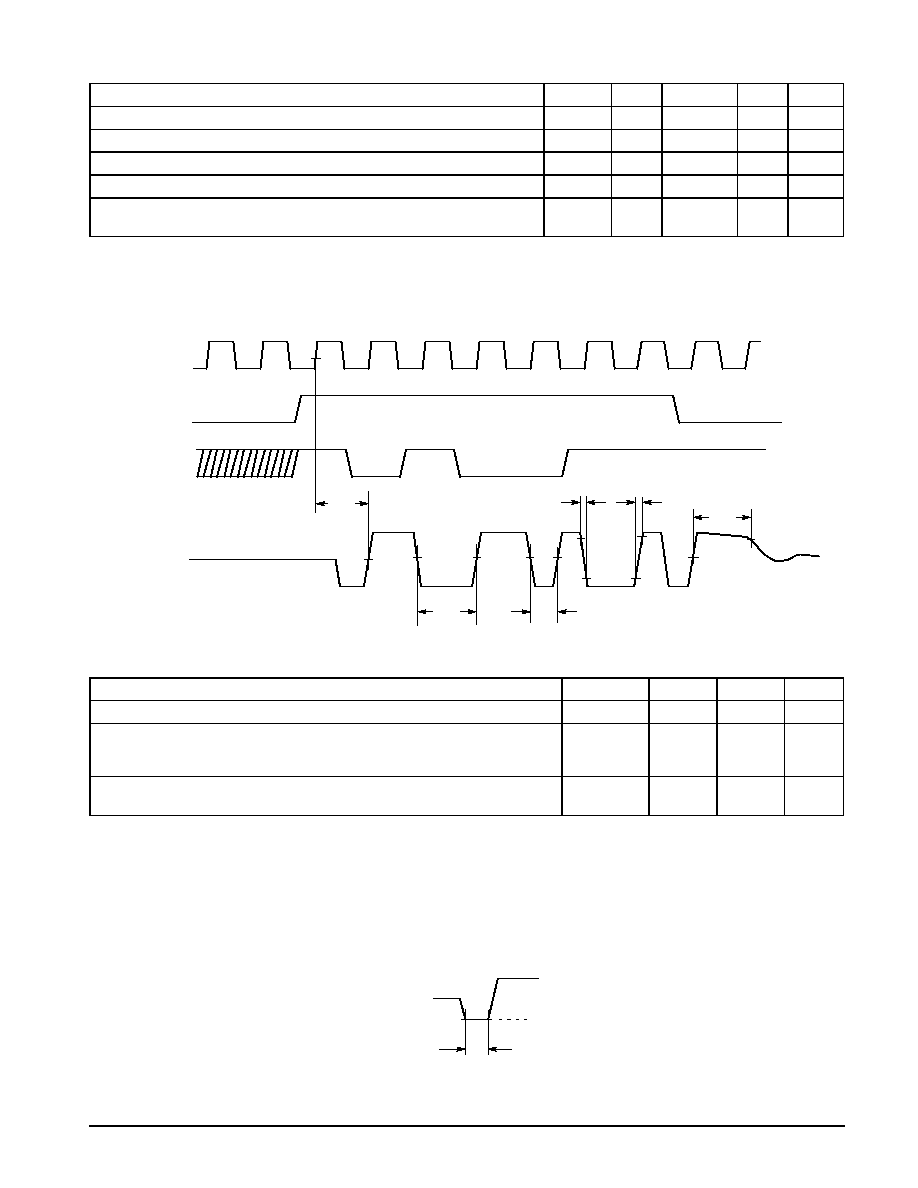
AUI TRANSMIT SWITCHING
Characteristic
Symbol
Min
Typ
Max
Unit
TCLK to ATX Pair Steady State Propagation Delay
t240
≠
≠
100
ns
Output Differential Rise and Fall Times (Measured directly at device pins)
t241
1.0
≠
5.0
ns
ATX Bit Cell Duration center≠to≠center (Measured directly at device pins)
t242
≠
99.5≠100.5
≠
ns
ATX Half≠Bit Cell Duration center≠to≠boundary (Measured directly at device pins)
t243
≠
49.5≠50.5
≠
ns
ATX Pair Held at Positive Differential at start of Idle (Measured through
transformer)
t244
200
≠
≠
ns
NOTE:
Load on specified output is a shunt 27
µ
H inductor and 83
resistor.
Figure 38. ATX Transmit Timings
1
0
1
TCLK
TENA
TX
ATX+/≠
Differential
(Logic Levels)
0
0
1
1
1
1
1
1
0
0
0
t240
0V
t242
t243
t241
t241
t244
90%
10%
90%
10%
0V
1.5V
70%
AUI RECEIVE SWITCHING
Characteristic
Symbol
Min
Max
Unit
ARX/ACX Differential Input Voltage Range
≠
±
318
±
1315
mV
ARX/ACX Differential Input Pulse Width to:
Initiate Data Reception
Inhibit Data Reception
t261
t262
30
≠
≠
18
ns
RENA Assertion Delay
RENA Deassertion Delay
t266
t267
≠
≠
100
450
ns
Squelching Characteristics
The receive data pairs and the collision pairs should have the following squelch characteristics:
1. The squelch circuits are on at idle (with input voltage at approximately 0 V differential).
2. If an input is in squelch, pulse is rejected if the peak differential voltage is more positive than ≠175 mV, regardless of pulse width.
3. A pulse is considered valid if its peak differential voltage is more negative than ≠300 mV and its width, measured at ≠285 mV, is > 25 ns.
4. The squelch circuits are disabled by the first valid negative differential pulse on either the AUI receive data or collision pair.
5. If a positive differential pulse occurs on either the AUI receive data or collision pair > 175 ns, end of frame is assumed and squelch circuitry is turned on.
t261/ t262
≠175mV
+175mV
ARX+/≠
ACX+/≠
Differential
Input Voltage
Figure 39. ARX/ACX Timing
MC68160A
25
MOTOROLA ANALOG IC DEVICE DATA
RENA/CLSN
1.5V
1.5V
≠300mV
1
0
1
0
0
1
1
10%
90%
90%
10%
0V
≠275mV
+300mV
Bit U
Bit V
Bit W
Bit X
Bit Z
Bit X
Bit Y
Bit Z
Bit U
RCLK
RX
Bit Y
Bit Q
Bit V
Bit U
Bit Q
Figure 40. ARX/ACX Timing
ARX+/≠/
ACX+/≠
Differential
Input Voltage
t261
t260
t266
t267
≠40mV
t260
FUNCTIONAL DESCRIPTION
Introduction
The MC68160A was designed to perform the physical
connection to the Ethernet media. This is done through two
separate media dependent interfaces and a SIA interface.
The media dependent interfaces are the Attachment Unit
Interface(AUI) and the 10BASE≠T Twisted Pair(TP) port. The
MC68160A's SIA interface is compatible with most industry
controllers and selected by three mode control pins. Chip
status is supported indicated by the condition of 6 status
indicator pins. All but one are open collector outputs.
If the EEST isn't receiving data, the controller may initiate
transmission. NRZ data from the communications controller
SIA interface is encoded by the MC68160A into Manchester
Code in preparation for transmission on the media. The data
is then applied to either the AUI or TP port. If the data was
transmitted using the 10BASE≠T port, this data is also
looped back to the receive data interface SIA pins
connected to the controller. This allows detection of a
collision condition in the event that another station on the
media attempted transmission at the same time. After the
entire data frame has been transmitted, the EEST must
force the media idle signal. The idle signal frees the media
for other stations that have deferred transmission. If no
other transmissions are required the link enters an idle
state. During this idle state the 10BASE≠T transmitter
issues idle pulses which communicates to the receiver
connected to the other side that the link is valid. If the
transmitter connected at the other end begins transmission,
the EEST will assert a receive enable signal, and forward
the received data to the controller.
Upon reception of data at the 10BASE≠T port, the data is
screened for proper sequence and pulse width requirements.
If the preamble of the received frame meets the
requirements, the PLL locks onto the 64≠bit preamble and
begins to decode the Manchester Code to NRZ code. This
code is then presented to the communications controller at
the receive data pins at the SIA interface. If data is received
at the AUI port, it is sent directly to the communications
controller via the SIA interface.
Data Transmission
To have properly encoded transmit data, the com≠
munications controller must be synchronized to TCLK.
Transmission to the 10BASE≠T or AUI media occurs when
TENA is asserted and data is applied to the TX pin. Finally, to
signify transmission, the TXLED in will cycle on and off at a
100 ms period. Data transmission for EEST is accomplished
either over the 10BASE≠T port or the AUI port. Both
connections to the media are made with industry standard
media interface components. The 10BASE≠T interface
requires a filter and transformer, the AUI interface requires
only a transformer. The filter for the 10BASE≠T transmit
circuit will have to be chosen for each application.

MC68160A
26
MOTOROLA ANALOG IC DEVICE DATA
If after approximately 40 ms after a TP or AUI transmission
has begun, the EEST is still transmitting, the TPJABB pin will
assert to signify a jabber condition. Also, the CLLED pin will
transition high and low alternately with a 100 ms period. The
transmit circuitry is, however, unaffected by the jabber
condition, so the communications controller has the
responsibility of monitoring and stopping transmission.
When transmission is complete, the transmit circuitry will
begin the end of transmit and decay to idle responses
necessary to meet requirements of the 802.3 standard for the
TP and AUI port.
Data Reception
Other than the case of being in Loop Back mode, data
reception to the RX pin of the EEST is initiated by signaling at
the RX+/≠ or AUI ARX+/≠ pins. If at the TP port, the data is
screened for validity by checking for sequence and pulse
width requirements, then passed to the decode and receive
circuitry. The RENA pin asserts and the data and
corresponding clock is passed to the communications
controller. After the frame has been transmitted, the
MC68160A detects the ending transmission and negates
RENA. If at the AUI port, the data is checked for proper pulse
width requirements before being passed to the decode
circuitry. If the data pulses are longer than at least 20 ns,
RENA gets asserted and the frame is decoded to RX with
and accompanying RCLK output.
Collision
Collision is the occurrence of simultaneous transmit
activity by two or more stations on the network. In the event of
collision, the data transfer paths are unaffected. If the
MC68160A is in the twisted pair mode, collision is detect by
simultaneous receive and transmit activity. If in the AUI
mode, collision is detected by activity on the ACX+/≠ pins. In
either case, if collision is detected, the CLSN pin will assert to
notify the communications controller.
Jabber
The EEST has a jabber timer to detect the jabber condition.
In the event that the transmitting station continues to transmit
beyond the allowable transmit time, a jabber timer (40 ms) will
expire and assert the TPJABB pin to alert the communications
controller of the situation. The TPJABB pin can source or sink
up to 10 mA, and so, is capable of driving a status LED. In the
AUI mode, the pin is driven to high impedance since the
transceiver connected to the AUI port must alert the
communications controller of the jabber condition.
Full Duplex
A feature unique to the MC68160A is the Full Duplex
mode. In this mode the EEST is capable of transmitting and
receiving simultaneously. Collision conditions are not
announced and internal loop back is disabled. The remainder
of the EEST functionality remains unchanged from the
non≠Full Duplex mode. Full Duplex mode is enabled by
asserting the TPFULDL pin.
Auto Port Selection
If the APORT pin is asserted, the MC68160A will
automatically select the TP or AUI port depending on the
presence of valid link beats or frames at the TP RX+/≠ pins. If
the AUI port is automatically selected by another transmitting
station or by setting TPEN low, the TP transmit port of the
EEST continues to transmit link beats to keep the link active.
Auto Polarity Selection
If the RX+ and the RX≠ wires happen to get reversed, the
MC68160A has the ability to automatically reverse the pins
internally so that the received data is valid. In addition, an open
collector status pin (TPPLR) is driven low to indicate the fault.
In the AUI or reset mode this pin presents a high impedance.
Loop Back Mode
To test the transmit and receive circuitry without disturbing
the connected network, the EEST has a Loop Back mode.
Loop Back mode routes transmit data and clock to the
receive data and clock pins using as much of the transmit and
receive circuitry as possible. This gives a test of the
MC68160A Manchester encode and decode function. LOOP
must not be asserted when TPFULDL pin is asserted. This
causes the MC68160A to enter a test mode. This test mode
is used during final test and is not intended to be entered
under normal operation (see Application Notes section).
MC68160A
27
MOTOROLA ANALOG IC DEVICE DATA
APPLICATIONS INFORMATION
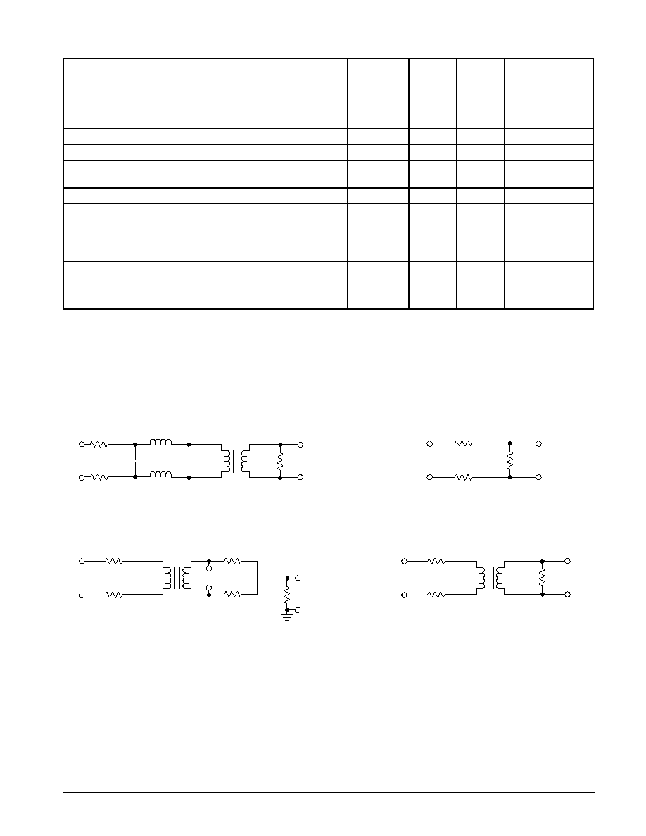
Selection of Crystal and External Components
Accuracy of frequency and stability over temperature are
the main determinants of crystal choice. Specifications for a
suitable crystal are tabulated below.
¡¡¡¡¡¡¡¡¡¡¡¡¡
¡¡¡¡¡¡¡¡¡¡¡¡¡
Frequency
¡¡¡¡¡
¡¡¡¡¡
20.000 MHz
¡¡¡¡¡¡¡¡¡¡¡¡¡
¡¡¡¡¡¡¡¡¡¡¡¡¡
Mode
¡¡¡¡¡
¡¡¡¡¡
Fundamental
¡¡¡¡¡¡¡¡¡¡¡¡¡
¡¡¡¡¡¡¡¡¡¡¡¡¡
Tolerance
¡¡¡¡¡
¡¡¡¡¡
±
100 ppm
¡¡¡¡¡¡¡¡¡¡¡¡¡
¡¡¡¡¡¡¡¡¡¡¡¡¡
Stability
¡¡¡¡¡
¡¡¡¡¡
±
100 ppm
¡¡¡¡¡¡¡¡¡¡¡¡¡
¡¡¡¡¡¡¡¡¡¡¡¡¡
Aging
¡¡¡¡¡
¡¡¡¡¡
±
5 ppm/yr
¡¡¡¡¡¡¡¡¡¡¡¡¡
¡¡¡¡¡¡¡¡¡¡¡¡¡
Shunt Capacitance
¡¡¡¡¡
¡¡¡¡¡
7.0 pF
¡¡¡¡¡¡¡¡¡¡¡¡¡
¡¡¡¡¡¡¡¡¡¡¡¡¡
Load Capacitance
¡¡¡¡¡
¡¡¡¡¡
18≠20 pF
¡¡¡¡¡¡¡¡¡¡¡¡¡
¡¡¡¡¡¡¡¡¡¡¡¡¡
Series Fundamental Resistance (ESR)
¡¡¡¡¡
¡¡¡¡¡
25
¡¡¡¡¡¡¡¡¡¡¡¡¡
¡¡¡¡¡¡¡¡¡¡¡¡¡
Drive Level
¡¡¡¡¡
¡¡¡¡¡
500
µ
W
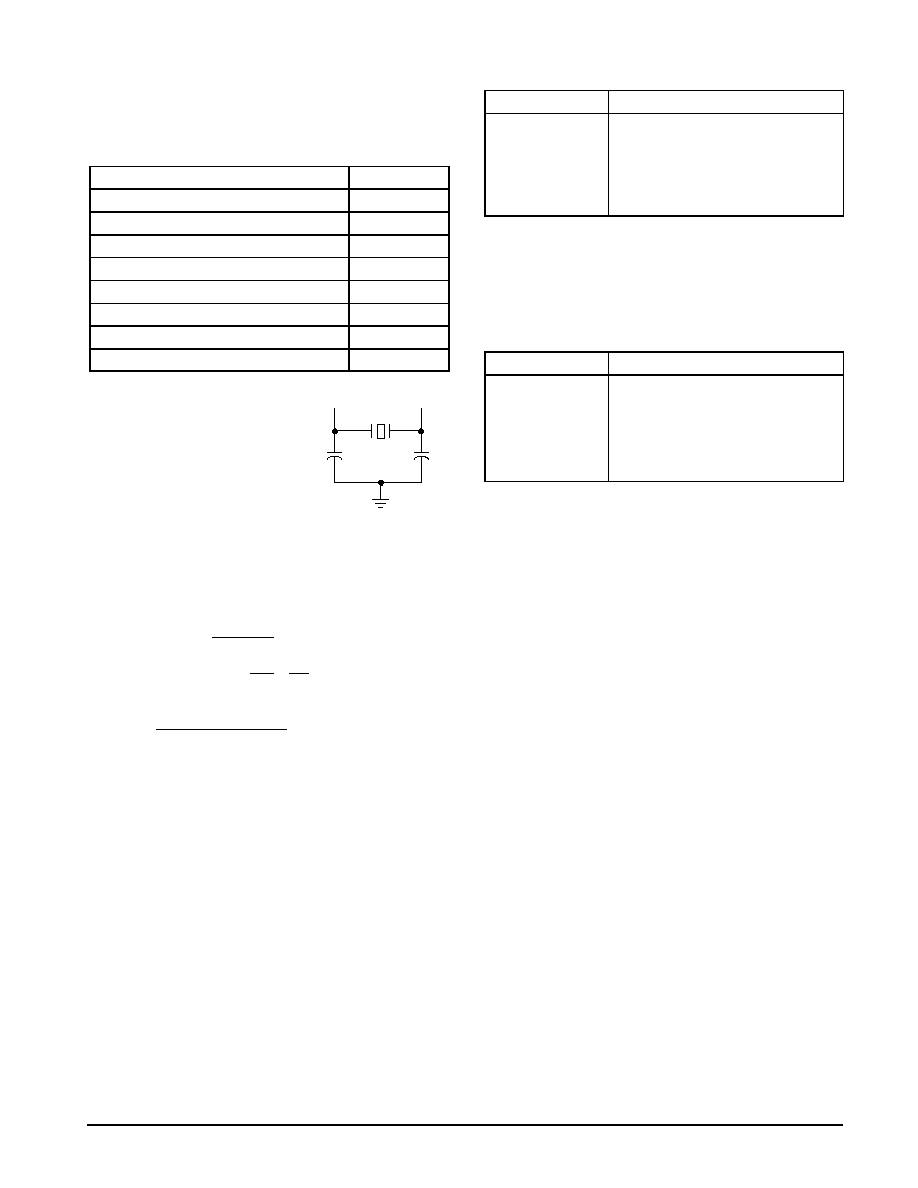
X1
X2
1
2
C5
C4
A suitable crystal is the MTRON
HC49 MP≠1, 20.000 MHz crystal.
20 pF for C4 and C5 have been
shown to work reliably.
PLL Filter Components
The filter components at Pin 12 were chosen to assure
adequate pull≠range but with a emphasis on stability. It is not
foreseeable that a design would need to change the
components, but for the sake of completeness, relevant
values are provided here.
VCO Gain
+
24
MHz
Volt
∑
sec
and,
Phase Detector Gain
+
100
p
2
m
A
rad
and the
filter impedance function is;
Z(j
w
)
[
(j
w )
1 C6)
j
w
∑
C5
∑
(j
w )
1 C5)
(for C6
uu
C5)
10BASE≠T Filter and Transformer Choice
The MC68160A differential outputs are low impedance
voltage sources. Therefore, external series resistors must be
used in order to match the characteristic impedance of
twisted pair. Since the output resistance of each leg of the
transmitter is about 10
, a 39
resistor is used in series as
shown in the applications schematic. So the impedance
presented from the source to the isolation transformer is then
very nearly 100
. The following is a list of some 10BASE≠T
filter module vendors and their products.
Vendor
Part #
FEE Fil≠Mag
78Z1120B≠01, 78Z1122B/D≠01,
78Z1122 F≠01
Valor Electronics
78Z1122 F≠01
PT3877, FL1012, FL1066
a o
ec o cs
Pulse Engineering
38
,
0
,
066
PE≠65434, PE65424, PE65433
TOKO
PM01≠00, PM02≠00, PM05≠00
AUI Transformer Choice
Like the 10BASE≠T outputs, the AUI differential outputs
are low impedance sources and capable of meeting the IEEE
802.3 waveform requirements when a coupling transformer
is used. Some AUI transformer vendors and their products
are provided below.
Vendor
Part #
Coilcraft
LAX≠ET304
FEE Fil≠Mag
23Z90, 23Z91/ 23Z92
Valor Electronics
LT6032, LT6033
Pulse Engineering
PE64502, PE6103
TOKO
Q30ALQ8≠1AA3, Q30ALQ9≠1AA3
Application Notes:
Resetting the MC68160A after power up.
In some applications, after initial power up, the MC68160A
may not be able to transmit or receive data. This is usually
caused by the LOOP and TPFULDL control lines being active
at the same time. This is an illegal condition during normal
operation, it places the MC68160A into the production test
mode.
To exit the test mode and return to normal: Set LOOP low,
TPFULDL high and TPSQEL low. Then, while keeping
TPSQEL low, raise LOOP after 300 ms lower TPFULDL. This
will put the MC68160A into test mode but also resets the
MC68160A. After 500 ms lower LOOP to get out of the test
mode. TPFULDL may then be de≠asserted if desired.
The MC68160A is now ready for operation.
A hardware implementation of this fix would be to place a
pull down resistor on the TPSQEL pin. Even if test mode is
entered by accident, this ensures that zero's will be written to
the test register. The hardware implementation will solve the
problem if the test mode is entered because of noise on the
TPSQEL pin. If the controller is toggling the MC68160A lines
while it is booting up, the reset procedure must be followed.
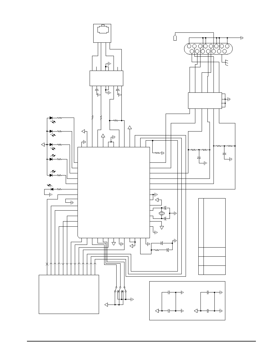
MC68160A
28
MOTOROLA ANALOG IC DEVICE DATA
1. For Suitable Crystal (X ) see applications text on previous page.
1
0.01 F
µ
17
15
41
40
42
52
51
50
49
48
47
46
45
44
43
25
26
24
14
16
18
19
20
21
22
23
ŒŒŒŒŒŒ
ŒŒŒŒŒŒ
ŒŒŒŒŒŒ
ŒŒŒŒŒŒ
ŒŒŒŒŒŒ
ŒŒŒŒŒŒ
TPEN
TCLK
TENA
TX
CLSN
RCLK
RENA
RX
LOOP
APOR
LED6
LED5
LED4
LED3
LED2
LED1
1
2
3
4
5
6
7
8
10
11
12
13
9
39
38
37
36
35
34
33
32
31
30
29
28
27
1
2
3
5
6
7
8
4
16
TD +
TD ≠
RD +
RD ≠
11
10
9
1
2
6
3
12
13
14
15
1
2
5
7
8
4
16
10
9
12
13
15
14
11
6
3
CS0
1
0
1
0
1
CS1
1
1
0
0
1
CS2
0
0
0
0
1
802.3 Communication Controller
Motorola
MC68360,
AMD 7990 & 79C900
Intel 82586, 82590, 82593, 82596
Fujitsu MB86950, MB86960
National 8390, 83C690, 83932B
Standby Low Current Mode
Communications Controller Selection
AUI XFMR
9
10
11
12
13
14
15
8
7
6
5
4
3
2
1
(Example of PE-65424)
RCLK
TENA
TX
CLSN
GNDCTL
TPEN
TCLK
TPLIL
CLLED
TPPLR
TXLED
GNDVCO
RXLED
X2
VDDDIG
GNDSUB
ACX≠
GNDDIG
X1
TPJABB
VDDVCO
ACX+
ARX+
ATX≠
ARX≠
ATX+
Figure 41. T
ypical
Application Diagram
TP
Enable
T
ransmit Clock
T
ransmit Enable
T
ransmit Data
Collision Int
Receive Clock
Receive Enable
Receive Data
LoopBack
AutoPort En
+5.0V
Power Supply
Bypassing
COMMUNICA
TIONS
CONTROLLER
MC68360
AMD (7990/79C900)
Intel (825** ≠86/90/93/96)
Fujitsu (869** ≠50/60)
National (8390/83C90/83932B)
V
CC
V
DD
10 F
µ
10 F
µ
0.1 F
µ
0.1 F
µ
V
CC
V
DD
TPSQEL
TPFULDL
TP
APCE
C
5
C
6
R
12
300
0.039 F
µ
V
DD
V
CC
CTP2
C
3
20pF
C
4
20pF
20MHz
X
1
RENA
RX
CS0
CS1
CS2
LOOP
VDDDIG
GNDDIG
APORT
VDDDIV
VDDFM
MFIL
T
GNDFM
GNDPWR
VDDPWR
TPTX+
TPTX≠
VDDPWR
GNDPWR
GNDANA
TPRX+
VDDANA
TP
APCE
TPFULDL
TPSQEL
TPRX≠
0.1 F
µ
0.1 F
µ
C
1
C
2
R
33
330
R
8
330
R
9
330
R
11
330
R
13
330
R
14
330
V
DD
V
DD
V
CC
R
3
100
R
4
39
R
5
39
R
6
39
R
7
39
Coilcraft (LAX≠ET30*)
Pulse Engineering (PE≠64***)
V
alor (L
T600*/L
T603*)
T
OKO (Q30ALQ*≠1AA3)
0.01 F
µ
CTP3
R
1
39
R
2
39
V
alor (PT3877, PT3882, FL1012, FL1066)
T
OKO (PM01, PM02, PM05)
Pulse Engineering (PE≠65433, PE≠65434, PE≠65424)
RJ45
+12V
AUI
V
DD
Figure 41.
MC68160AFB
3900pF
2. Decoupling capacitors should be placed as close to supply pins as possible.
R
15
10 K
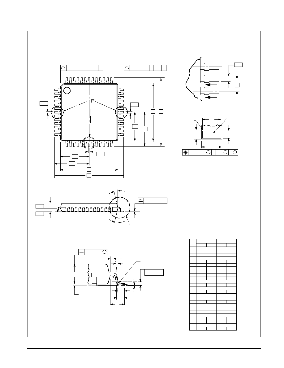
MC68160A
29
MOTOROLA ANALOG IC DEVICE DATA
FB SUFFIX
PLASTIC PACKAGE
CASE 848D-03
(LQFP≠52)
ISSUE C
OUTLINE DIMENSIONS
F
NOTES:
1 DIMENSIONING AND TOLERANCING PER ANSI Y14.5M, 1982.
2 CONTROLLING DIMENSION: MILLIMETER.
3 DATUM PLANE ≠H≠ IS LOCATED AT BOTTOM OF LEAD AND
IS COINCIDENT WITH THE LEAD WHERE THE LEAD EXITS
THE PLASTIC BODY AT THE BOTTOM OF THE PARTING
LINE.
4 DATUMS ≠L≠, ≠M≠ AND ≠N≠ TO BE DETERMINED AT DATUM
PLANE ≠H≠.
5 DIMENSIONS S AND V TO BE DETERMINED AT SEATING
PLANE ≠T≠.
6 DIMENSIONS A AND B DO NOT INCLUDE MOLD
PROTRUSION. ALLOWABLE PROTRUSION IS 0.25 (0.010)
PER SIDE. DIMENSIONS A AND B DO INCLUDE MOLD
MISMATCH AND ARE DETERMINED AT DATUM PLANE -H-.
7 DIMENSION D DOES NOT INCLUDE DAMBAR PROTRUSION.
DAMBAR PROTRUSION SHALL NOT CAUSE THE LEAD
WIDTH TO EXCEED 0.46 (0.018). MINIMUM SPACE BETWEEN
PROTRUSION AND ADJACENT LEAD OR PROTRUSION 0.07
(0.003).
…………
…………
«««
«««
VIEW AA
VIEW AA
2 X R
R1
AB
AB
VIEW Y
SECTION AB≠AB
ROTATED 90
_
CLOCKWISE
DIM
A
MIN
MAX
MIN
MAX
INCHES
10.00 BSC
0.394 BSC
MILLIMETERS
A1
5.00 BSC
0.197 BSC
B
10.00 BSC
0.394 BSC
B1
5.00 BSC
0.197 BSC
C
≠≠≠
1.70
≠≠≠
0.067
C1
0.05
0.20
0.002
0.008
C2
1.30
1.50
0.051
0.059
D
0.20
0.40
0.008
0.016
E
0.45
0.030
F
0.22
0.35
0.009
0.014
G
0.65 BSC
0.75
0.018
0.026 BSC
J
0.07
0.20
0.003
0.008
K
0.50 REF
0.020 REF
R1
0.08
0.20
0.003
0.008
S
12.00 BSC
0.472 BSC
S1
6.00 BSC
0.236 BSC
U
0.09
0.16
0.004
0.006
V
12.00 BSC
0.472 BSC
V1
6.00 BSC
0.236 BSC
W
0.20 REF
0.008 REF
Z
1.00 REF
0.039 REF
CL
≠X≠
X=L, M, N
1
13
14
26
27
39
40
52
4X TIPS
4X
N
0.20 (0.008) H L≠M
N
0.20 (0.008) T L≠M
3X
VIEW Y
SEATING
PLANE
C
0.10 (0.004) T
4X
3
4X
2
S
0.05 (0.002)
0.25 (0.010)
GAGE PLANE
C2
C1
W
K
E
Z
S
L≠M
M
0.13 (0.005)
N
S
T
PLATING
BASE METAL
D
J
U
B
V
B1
A
S
V1
A1
S1
≠L≠
≠N≠
≠M≠
≠H≠
≠T≠
1
G
1
3
2
0
7
_
_
12
5
13
_
_
_
0
7
_
_
0
_
0
_
≠≠≠
≠≠≠
REF
12
_
REF
13
_
5
_

MC68160A
30
MOTOROLA ANALOG IC DEVICE DATA
NOTES

MC68160A
31
MOTOROLA ANALOG IC DEVICE DATA
NOTES

MC68160A
32
MOTOROLA ANALOG IC DEVICE DATA
Motorola reserves the right to make changes without further notice to any products herein. Motorola makes no warranty, representation or guarantee regarding
the suitability of its products for any particular purpose, nor does Motorola assume any liability arising out of the application or use of any product or circuit, and
specifically disclaims any and all liability, including without limitation consequential or incidental damages. "Typical" parameters which may be provided in Motorola
data sheets and/or specifications can and do vary in different applications and actual performance may vary over time. All operating parameters, including "Typicals"
must be validated for each customer application by customer's technical experts. Motorola does not convey any license under its patent rights nor the rights of
others. Motorola products are not designed, intended, or authorized for use as components in systems intended for surgical implant into the body, or other
applications intended to support or sustain life, or for any other application in which the failure of the Motorola product could create a situation where personal injury
or death may occur. Should Buyer purchase or use Motorola products for any such unintended or unauthorized application, Buyer shall indemnify and hold Motorola
and its officers, employees, subsidiaries, affiliates, and distributors harmless against all claims, costs, damages, and expenses, and reasonable attorney fees
arising out of, directly or indirectly, any claim of personal injury or death associated with such unintended or unauthorized use, even if such claim alleges that
Motorola was negligent regarding the design or manufacture of the part. Motorola and are registered trademarks of Motorola, Inc. Motorola, Inc. is an Equal
Opportunity/Affirmative Action Employer.
Mfax is a trademark of Motorola, Inc.
How to reach us:
USA / EUROPE / Locations Not Listed: Motorola Literature Distribution;
JAPAN: Nippon Motorola Ltd.; Tatsumi≠SPD≠JLDC, 6F Seibu≠Butsuryu≠Center,
P.O. Box 5405, Denver, Colorado 80217. 303≠675≠2140 or 1≠800≠441≠2447
3≠14≠2 Tatsumi Koto≠Ku, Tokyo 135, Japan. 81≠3≠3521≠8315
Mfax
TM
: RMFAX0@email.sps.mot.com ≠ TOUCHTONE 602≠244≠6609
ASIA/PACIFIC: Motorola Semiconductors H.K. Ltd.; 8B Tai Ping Industrial Park,
≠ US & Canada ONLY 1≠800≠774≠1848
51 Ting Kok Road, Tai Po, N.T., Hong Kong. 852≠26629298
INTERNET: http://www.mot.com/SPS/
MC68160A/D