4707 Dey Road Liverpool, N.Y. 13088
M.S.KENNEDY CORP.
(315) 701-6751
FEATURES:
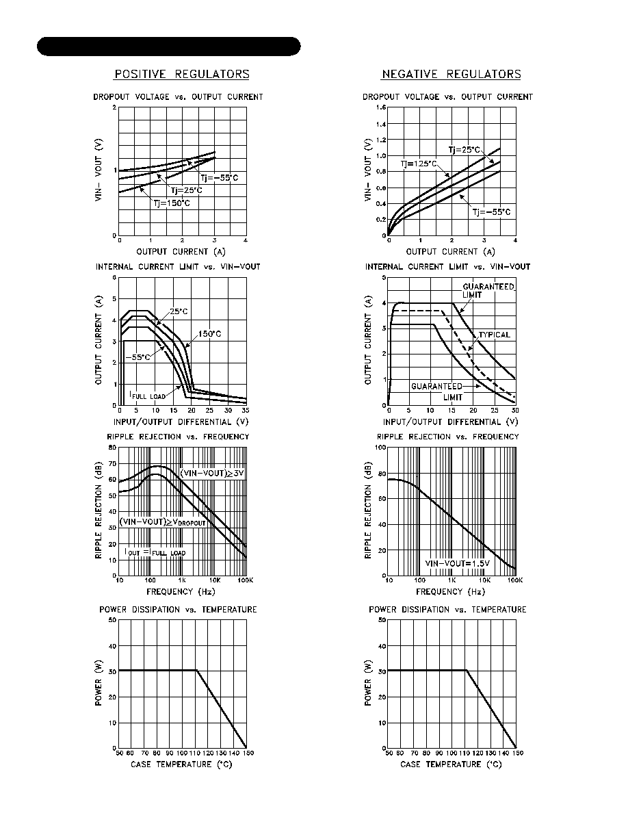
Dual Low Dropout Voltage
Internal Short Circuit Current Limit
Output Voltages Are Internally Set To ±1% Max
Electrically Isolated Case
Internal Thermal Overload Protection
Many Output Voltage Combinations
Available Fully Qualified to Mil-PRF-38534
Alternate Package and Lead Form Configurations Available
High Efficiency Linear Regulators
Constant Voltage/Current Regulators
System Power Supplies
Switching Power Supply Post Regulators
TYPICAL APPLICATIONS
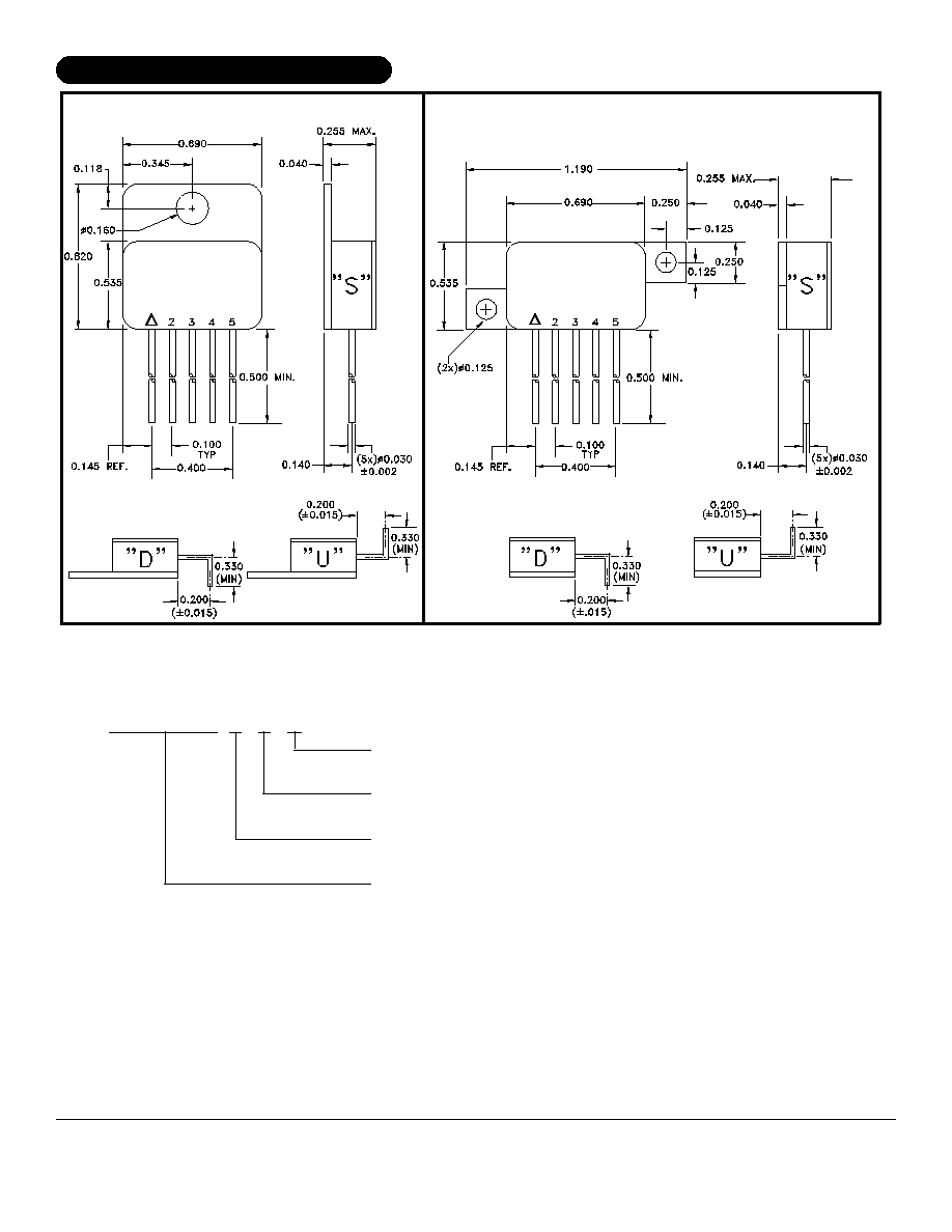
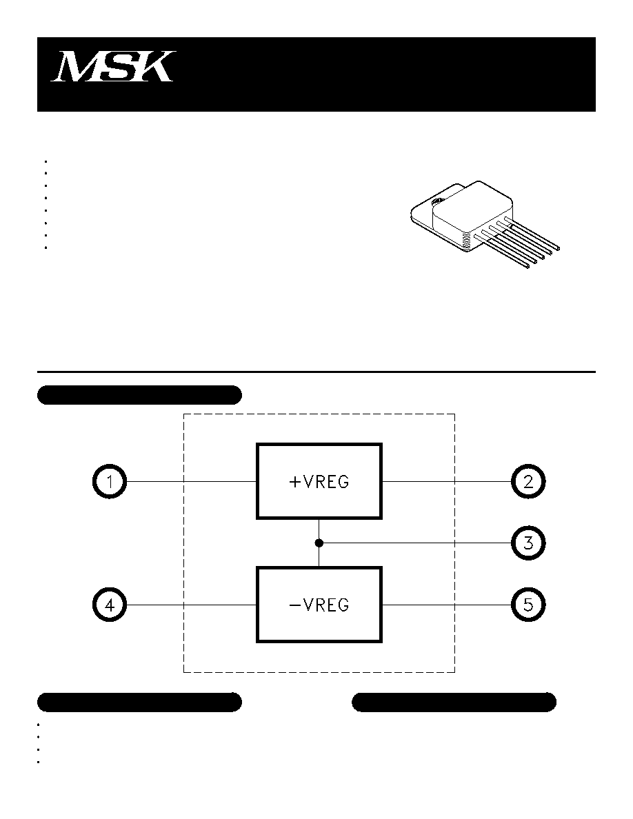
PIN-OUT INFORMATION
1
2
3
4
5
+Vin
+Vout
GND
-Vin
-Vout
5000
SERIES
DUAL POSITIVE/NEGATIVE,
3 AMP, LOW DROPOUT
FIXED VOLTAGE REGULATORS
DESCRIPTION:
The MSK 5000 Series offers low dropout voltages on both the positive and negative regulators. This, combined
with the low
JC,
allows increased output current while providing exceptional device efficiency. Because of the
increased efficiency, a small hermetic 5 pin package can be used providing maximum performance while occupying
minimal board space. Output voltages are internally trimmed to ±1% maximum resulting in consistent and accurate
operation. Additionally, both regulators offer internal short circuit current and thermal limiting, which allows circuit
protection and eliminates the need for external components and excessive derating.
ISO-9001 CERTIFIED BY DSCC
EQUIVALENT SCHEMATIC
MIL-PRF-38534 CERTIFIED
1
Rev. E 7/00
PART
NUMBER
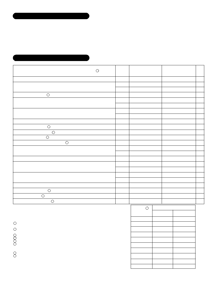
POSITIVE OUTPUT REGULATORS:
Output Voltage Tolerance
Dropout Voltage
Load Regulation
Line Regulation
Quiescent Current
Short Circuit Current
Ripple Rejection
Thermal Resistance
NEGATIVE OUTPUT REGULATORS:
Output Voltage Tolerance
Dropout Voltage
Load Regulation
Line Regulation
Quiescent Current
Short Circuit Current
Ripple Rejection
Thermal Resistance 2
Max.
1.0
2.0
1.5
1
2
0.5
.75
15
-
-
2.7
1.0
2.0
1.2
1
2
.5
.75
10
-
-
2.2
Storage Temperature Range
Lead Temperature Range
(10 Seconds)
Case Operating Temperature
MSK 5000-5009
MSK 5000B-5009B
±30V
Internally Limited
±3A
+175∞C
-65∞C to +150∞C
300∞C
-40∞C to +85∞C
-55∞C to +125∞C
ABSOLUTE MAXIMUM RATINGS
T
ST
T
LD
T
C
Input Voltage (WRT V
OUT
)
Power Dissipation
Output Current
Junction Temperature
±V
IN
P
D
I
OUT
T
J
Outputs are decoupled to ground using 10µF minimum
low ESR capacitors unless otherwise specified.
This parameter is guaranteed by design but need not be tested.
Typical parameters are representative of actual device performance but are for reference only.
All output parameters are tested using a low duty cycle pulse to maintain T
J
= T
C
.
Industrial grade devices shall be tested to subgroup 1 unless otherwise specified.
Military grade devices ('B' suffix) shall be 100% tested to subgroups 1,2 and 3.
Subgroup 1 T
A
=T
C
=+25∞C
Subgroup 2 T
A
=T
C
=+125∞C
Subgroup 3 T
A
=T
C
=-55∞C
Min.
-
-
-
-
-
-
-
-
3.0
60
-
-
-
-
-
-
-
-
-
3.0
60
-
Group A
Subgroup
1
2,3
1
1
2,3
1
2,3
1,2,3
-
-
-
1
2,3
1
1
2,3
1
2,3
1,2,3
-
-
-
Min.
-
-
-
-
-
-
-
-
3.2
60
-
-
-
-
-
-
-
-
-
3.3
60
-
Typ.
0.1
0.1
1.3
0.2
0.3
0.1
0.2
10
4
75
2.5
0.1
0.1
0.8
0.2
0.3
.1
.2
4.5
3.6
75
2.0
Typ.
0.1
-
1.3
0.2
-
0.1
-
10
4
75
2.5
0.1
-
0.8
0.2
-
.1
-
4.5
3.6
75
2.0
Max.
2.0
-
1.6
2
-
0.6
-
15
-
-
2.7
2.0
-
1.3
2
-
.6
-
10
-
-
2.2
Parameter
ELECTRICAL SPECIFICATIONS
Test Conditions
Units
MSK 5000 SERIES
MSK 5000(B) SERIES
3
2
2
2
2
I
OUT
=0A; V
IN
=V
OUT
+3V
0A
I
OUT
3A;
V
OUT
=50mV
100mA
I
OUT
3A
V
IN
=V
OUT
+3V
I
OUT
=0A
(V
OUT
+3V)
V
IN
(V
OUT
+15V)
V
IN
=V
OUT
+3V; I
OUT
=0A
V
IN
=V
OUT
+5V
I
OUT
=3A; C
OUT
=25µF; f=120Hz
JUNCTION TO CASE
I
OUT
=0A; V
IN
=V
OUT
+3V
0A
I
OUT
3A;
V
OUT
=50mV
V
IN
=V
OUT
+3V
100mA
I
OUT
3A
I
OUT
=0A
(V
OUT
+3V)
V
IN
(V
OUT
+15V)
V
IN
=V
OUT
+3V; I
OUT
=0A
V
IN
=V
OUT
+5V
I
OUT
=3A; C
OUT
=25µF; f=120Hz
JUNCTION TO CASE
%
%
V
%
%
%
%
mA
A
dB
∞C/W
%
%
V
%
%
%
%
mA
A
dB
∞C/W
+ 3 . 3 V
+ 5 . 0 V
+ 5 . 0 V
+ 1 2 . 0 V
+ 1 2 . 0 V
+ 1 5 . 0 V
+ 1 5 . 0 V
+ 5 . 0 V
+ 5 . 0 V
+ 1 0 . 0 V
MSK5000(B)
MSK5001(B)
MSK5002(B)
MSK5003(B)
MSK5004(B)
MSK5005(B)
MSK5006(B)
MSK5007(B)
MSK5008(B)
MSK5009(B)
- 5 . 2 V
- 5 . 0 V
- 5 . 2 V
- 5 . 0 V
- 1 2 . 0 V
- 1 5 . 0 V
- 5 . 0 V
- 1 2 . 0 V
- 1 5 . 0 V
- 1 0 . 0 V
8
OUTPUT VOLTAGES
POSITIVE NEGATIVE
7
2
2
Rev. E 7/00
Please consult the factory if alternate output voltages are required.
Input voltage (V
IN
= V
OUT
+ a specified voltage) is implied to be more negative than V
OUT
.
1
2
3
4
5
6
7
8
2
APPLICATION NOTES
HEAT SINKING
To determine if a heat sink is required for your application
and if so, what type, refer to the thermal model and govern-
ing equation below.
Governing Equation: Tj = Pd x (R
jc + R
cs + R
sa) + Ta
WHERE
Tj = Junction Temperature
Pd = Total Power Dissipation
R
jc = Junction to Case Thermal Resistance
R
cs = Case to Heat Sink Thermal Resistance
R
sa = Heat Sink to Ambient Thermal Resistance
Tc = Case Temperature
Ta = Ambient Temperature
Ts = Heat Sink Temperature
EXAMPLE:
This example demonstrates an analysis where each regulator
is at one-half of its maximum rated power dissipation, which
occurs when the output currents are at 1.5 amps each.
Conditions for MSK 5002:
Vin = ±7.0V; Iout = ±1.5A
1.) Assume 45∞ heat spreading model.
2.) Find positive regulator power dissipation:
Pd = (Vin - Vout)(Iout)
Pd = (7-5)(1.5)
= 3.0W
3.) For conservative design, set Tj = +125∞C Max.
4.) For this example, worst case Ta = +90∞C.
5.) R
jc = 2.5∞C/W from the Electrical Specification Table.
6.) R
cs = 0.15∞C/W for most thermal greases.
7.) Rearrange governing equation to solve for R
sa:
R
sa= ((Tj - Ta)/Pd) - (R
jc) - (R
cs)
= (125∞C - 90∞C)/3.0W - (2.5∞C/W - 0.15∞C/W)
= 9.32∞C/W
The same exercise must be performed for the negative regula-
tor. In this case the result is 9.32∞C/W. Therefore, a heat sink
with a thermal resistance of no more than 9.3∞C/W must be
used in this application to maintain both regulator circuit junc-
tion temperatures under 125∞C.
OVERLOAD SHUTDOWN
The regulators feature both power and thermal overload pro-
tection. When the maximum power dissipation is not exceeded,
the regulators will current limit slightly above their 3 amp rating.
As the Vin-Vout voltage increases, however, shutdown occurs in
relation to the maximum power dissipation curve. If the device
heats enough to exceed its rated die junction temperature due to
excessive ambient temperature, improper heat sinking etc., the
regulators also shutdown until an appropriate junction tempera-
ture is maintained. It should also be noted that in the case of an
extreme overload, such as a sustained direct short, the device
may not be able to recover. In these instances, the device must
be shut off and power reapplied to eliminate the shutdown con-
dition.
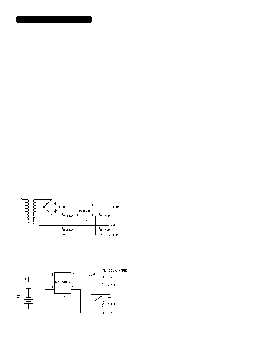
LOAD REGULATION
For best results the ground pin should be connected directly to
the load as shown below, this effectively reduces the ground
loop effect and eliminates excessive voltage drop in the sense
leg. It is also important to keep the output connection between
the regulator and the load as short as possible since this directly
affects the load regulation. For example, if 20 gauge wire were
used which has a resistance of about .008 ohms per foot, this
would result in a drop of 8mV/ft at 1Amp of load current. It is
also important to follow the capacitor selection guidelines to
achieve best performance. Refer to Figure 2 for connection dia-
gram.
FIGURE 2
Avoiding Ground Loops
BYPASS CAPACITORS
For most applications a 10uF minimum, low ESR (0.5-2 ohm)
tantalum capacitor should be attached as close to the regulator's
output as possible. This will effectively lower the regulator's
output impedance, increase transient response and eliminate any
oscillations that are normally associated with low dropout regu-
lators. Additional bypass capacitors can be used at the remote
load locations to further improve regulation. These can be either
of the tantalum or the electrolytic variety. Unless the regulator
is located very close to the power supply filter capacitor(s), a
4.7uF minimum low ESR (0.5-2 ohm) tantalum capacitor should
also be added to the regulator's input. An electrolytic may also
be substituted if desired. When substituting electrolytic in place
of tantalum capacitors, a good rule of thumb to follow is to
increase the size of the electrolytic by a factor of 10 over the
tantalum value.
Low Dropout Positive and Negative Power Supply
MSK 5002 TYPICAL APPLICATION:
FIGURE 1
3
Rev.E 7/00