4707 Dey Road Liverpool, N.Y. 13088
(315) 701-6751
MIL-PRF-38534 QUALIFIED
Servo Amplifer
Motor Driver
Audio Amplifier
Programmable Power Supply
TYPICAL APPLICATIONS
1 Current Sense
5 Inverting Input
2 No Connection
6 Negative Power Supply
3 Positive Power Supply
7 No Connection
4 Non-Inverting Input
8 Output Drive
1
PIN-OUT INFORMATION
Rev. C 3/01
ISO 9001 CERTIFIED BY DSCC
The above pin out table is for the MSK 541 (TO-3). Refer to the
mechanical specifications page for the pin out information of addi-
tional package styles.
FEATURES:
Available as SMD #5962-8870101
High Output Current - 10 Amps Peak
Wide Power Supply Range - �10V to �40V
Programmable Current Limit
FET Input
Isolated Case
Replacement for OMA 541SKB - MSK 541
OMA 541SDB - MSK 146
OMA 541SZB - MSK 147
DESCRIPTION:
The MSK 541 Series is a high power monolithic amplifier ideally suited for high power amplification and magnetic
deflection applications. This amplifier is capable of operation at a supply voltage rating of 80 volts and can deliver
guaranteed continuous output currents up to 5A, making the 541 series an excellent low cost choice for motor drive
circuits. The amplifier and load can be protected from fault conditions through the use of internal current limit
circuitry that can be user programmed with a single external resistor. The MSK 541 is pin compatible with popular
op-amps such as the Burr-Brown OPA501, OPA511, OPA512, OPA541 and 3573. The MSK 541 is available in a
hermetically sealed 8 pin TO-3 package. Other package styles are also available for a wide range of applications.
The MSK 145 is available in a 6 pin SIP Package. The MSK 146 is an 8 pin Power DIP Package and the MSK 147
is available in an 8 pin Power Z-TAB Package for applications requiring bolt down heat sinking.
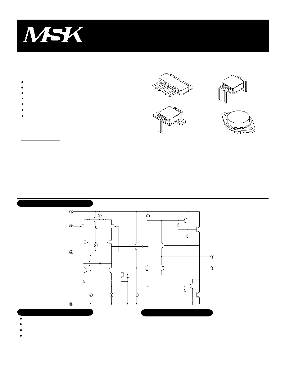
EQUIVALENT SCHEMATIC
MSK147
MSK145
MSK541
MSK146
HIGH POWER
OP-AMP
MSK 541 ONLY
M.S KENNEDY CORP.
541
SERIES
HIGH POWER
OP-AMP
Group A
Subgroup
-
1, 2, 3
1
2, 3
1
2, 3
1
2, 3
-
-
-
-
-
4
5, 6
4
5, 6
-
4
4
4
5, 6
STATIC
Supply Voltage Range
Quiescent Current
INPUT
Input Offset Voltage
Input Offset Voltage Drift
Input Capacitance
Input Impedance
Common Mode Rejection Ratio
Power Supply Rejection Ratio
Input Noise Voltage
OUTPUT
Settling Time
Power Bandwidth
TRANSFER CHARACTERISTICS
Slew Rate
Max.
�40
�35
�10
-
�100
-
30
-
-
-
-
-
-
-
-
-
-
-
-
-
-
-
Typ.
�35
�20
�1.0
�15
�4
�0.2
2.0
-
5
10
12
113
90
10
�29
-
�8
-
2
50
10
100
-
Min.
�10
-
-
-
-
-
-
-
-
-
90
-
-
�28
-
�5
-
-
40
6
90
-
Max.
�40
�30
�1.0
�50
�50
�10
30
20
-
-
-
-
-
-
-
-
-
-
-
-
-
-
Typ.
�35
�20
�0.1
�15
�4
�0.2
2.0
-
5
10
12
113
90
10
�29
�31
�8
-
2
55
10
100
-
Min.
�10
-
-
-
-
-
-
-
-
-
95
-
-
�28
�30
�5
�3.0
-
45
6
95
85
V
IN
= 0V
V
IN
= 0V
V
IN
= 0V
V
CM
= 0V
Either Input
F = DC
F = DC V
CM
= �22V
V
CC
= �10V to �40V
F = 10 Hz to 1 KHz
R
L
= 5.6
F = 10 KHz
R
L
=10
F = 10 KHz
R
L
= 5.6
F =10 KHz
R
L
= 10
F = 10 KHz
0.1% 2V step
R
L
= 10
V
O
= 20 V
RMS
V
OUT
= �10V R
L
= 10
�V
CC
Supply Voltage
�40V
I
OUT
Peak Output Current See S.O.A.
V
IN
Differential Input Voltage
�V
CC
V
IN
Common Mode Input Voltage
�V
CC
R
TH
Thermal Resistance-Junction to Case
MSK 541
1.9� C/W
MSK 145 1.2� C/W
MSK 146 1.2� C/W
MSK 147 1.2� C/W
ABSOLUTE MAXIMUM RATINGS
ELECTRICAL SPECIFICATIONS
T
ST
Storage Temperature Range
-65� to +150�C
T
LD
Lead Temperature Range 300�
(10 Seconds)
P
D
Power Dissipation 125W
T
J
Junction Temperature
150�C
T
C
Case Operating Temperature Range
Military Versions -55�C to +125�C
Industrial Versions -40�C to +85�C
Units
V
mA
mV
�V/�C
pA
nA
pA
nA
pF
W
dB
dB
�V
RMS
V
V
A
A
�S
KHz
V/�S
dB
dB
NOTES:
1
Unless otherwise specified R
CL
= 0
, �V
CC
= �34 V
DC
2
Electrical specifications are derated for power supply voltages other than �34 V
DC
.
3
AV = -1, measured in false summing junction circuit.
4
Devices shall be capable of meeting the parameter, but need not be tested. Typical parameters are for reference only.
5
Industrial grade devices shall be tested to subgroups 1 and 4 unless otherwise specified.
6
Military grade devices ('B' suffix) shall be 100% tested to subgroups 1, 2, 3 and 4.
7
Subgroup 5 and 6 testing available upon request.
8
Subgroup 1, 4
T
A
= T
C
= +25�C
Subgroup 2, 5
T
A
= T
C
= +125�C
Subgroup 3, 6
T
A
= T
C
= -55�C
Rereference DSCC SMD 5962-8870101 for electrical specifications for devices purchased as such.
3
4
2
Rev. C 3/01
Military
Industrial
2
4
V
CM
=0V
Input Offset Current
Input Bias Current
Output Voltage Swing
Output Current
Open Loop Voltage Gain
F = 10 H
Z
R
L
= 10 K
Parameter
Test Conditions
5
9
4
4
4
4
9

HEAT SINKING
To select the correct heat sink for your application, refer to the
thermal model and governing equation below.
Thermal Model:
Governing Equation:
T
J
= P
D
X (R
JC
+ R
CS
+ R
SA
) + T
A
Where
T
J
= Junction Temperature
P
D
= Total Power Dissipation
R
JC
= Junction to Case Thermal Resistance
R
CS
= Case to Heat Sink Thermal Resistance
R
SA
= Heat Sink to Ambient Thermal Resistance
T
C
= Case Temperature
T
A
= Ambient Temperature
T
S
= Sink Temperature
Example:
(TO-3 PACKAGE)
In our example the amplifier application requires the output to
drive a 20 volt peak sine wave across a 5 ohm load for 4 amps of
output current. For a worst case analysis we will treat the 4 amps
peak output current as a D.C. output current. The power supplies
are �35 VDC.
1.) Find Power Dissipation
P
D
= [(quiescent current) X (+V
CC
- (V
CC
))] + [(V
S
- V
O
) X I
OUT
]
= (30 mA) X (70V) + (15V) X (4A)
= 2.1W + 60W
= 62.1W
2.) For conservative design, set T
J
= +150�C
3.) For this example, worst case T
A
= +25�C
4.) R
JC
= 1.2�C/W typically for the TO-3 package
5.) R
CS
= 0.15�C/W for most thermal greases
6.) Rearrange governing equation to solve for R
SA
R
SA
= (T
J
- T
A
) / P
D
- (R
JC
) - (R
CS
)
= (150�C - 25�C) / 62.1W - (1.2�C/W) - (0.15�C/W)
= 0.66�C/W
The heat sink in this example must have a thermal resistance of
no more than 0.66�C/W to maintain a junction temperature of no
more than +150�C. Since this value of thermal resistance may be
difficult to find, other measures may have to be taken to decrease
the overall power dissipation.
APPLICATION NOTES
CURRENT LIMIT
The MSK 541 has an on-board current limit scheme designed
to limit the output drivers anytime output current exceeds a
predetermined limit. The following formula may be used to
determine the value of the current limit resistance necessary to
establish the desired current limit.
R
CL
(OHMs) = (0.809 volts / current limit in amps) - 0.057 OHM
The 0.057 OHM term takes into account any wire bond and
lead resistance. Since the 0.809 volt term is obtained from the
base emitter voltage drop of a bipolar transistor, the equation
only holds true for operation at +25�C case temperature. The
effect that temperature has on current limit may be seen on the
Current Limit vs. Case Temperature Curve in the Typical Perfor-
mance Curves.
Current Limit Connection
See "Application Circuits" in this data sheet for additional
information on current limit connections.
POWER SUPPLY BYPASSING
Both the negative and the positive power supplies must be
effectively decoupled with a high and low frequency bypass
circuit to avoid power supply induced oscillation. An effective
decoupling scheme consists of a 0.1 microfarad ceramic ca-
pacitor in parallel with a 4.7 microfarad tantalum capacitor from
each power supply pin to ground. It is also a good practice
with very high power op-amps, such as the MSK 541, to place
a 30-50 microfarad nonelectrolytic capacitor with a low effec-
tive series resistance in parallel with the other two power sup-
ply decoupling capacitors. This capacitor will eliminate any
peak output voltage clipping which may occur due to poor
power supply load regulation. All power supply decoupling
capacitors should be placed as close to the package power
supply pins as possible (pins 3 and 6 for the MSK 541).
SAFE OPERATING AREA
The safe operating area curve is a graphical representation of
the power handling capability of the amplifier under various
conditions. The wire bond current carrying capability, transis-
tor junction temperature and secondary breakdown limitations
are all incorporated into the safe operating area curves. All
applications should be checked against the S.O.A. curves to
ensure high M.T.B.F.
3
Rev. C 3/01
4
Rev. C 3/01
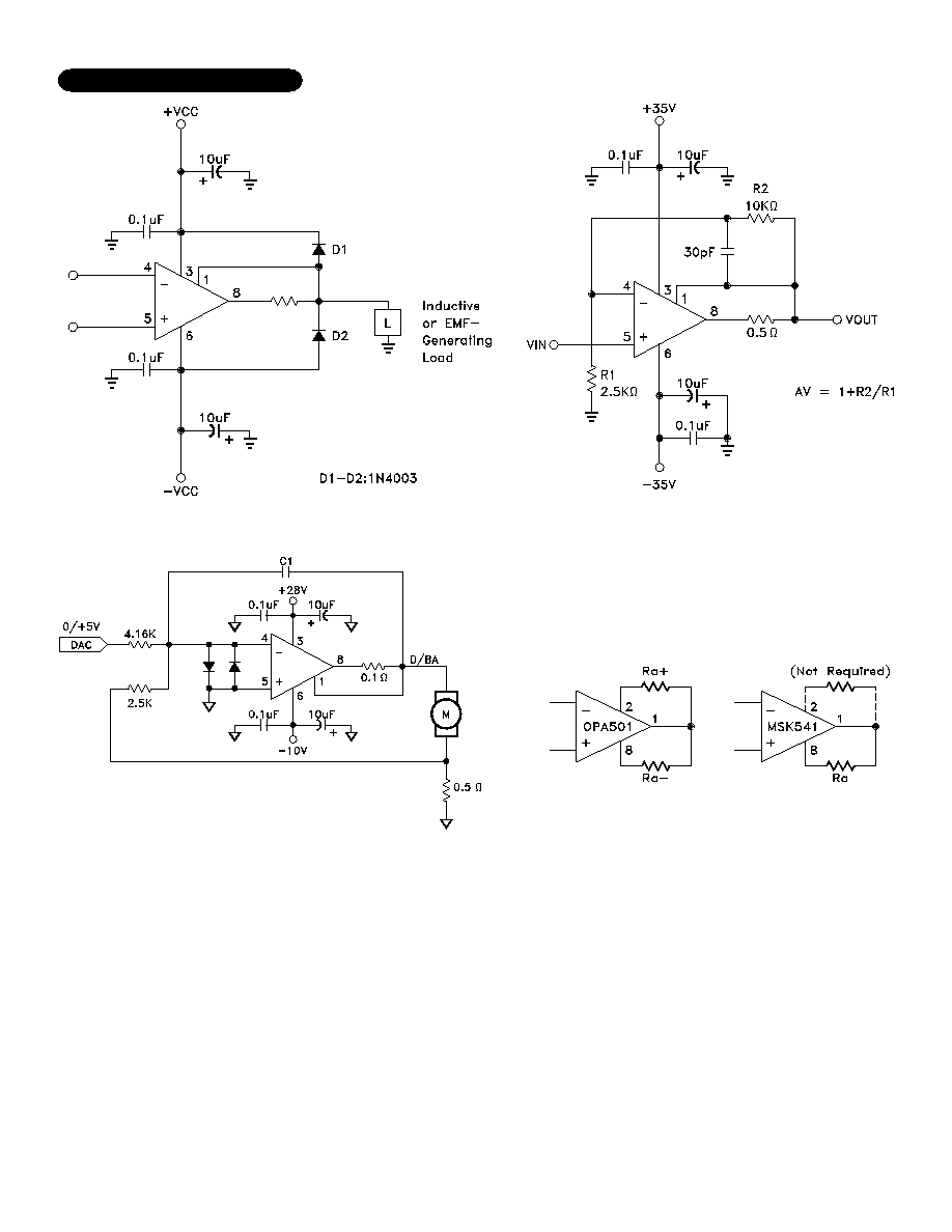
APPLICATION CIRCUITS
Isolating Capacitive Loads
Motor Current a Function of V
IN
Programmable Torque Circuit
Clamping Output for EMF-Generating Loads
The linear relationship of torque output to current input
of the modern torque motor makes this simple control cir-
cuit ideal for many material processing and testing appli-
cations. The sense resistor develops a feedback voltage
proportional to motor current and the small signal proper-
ties of the Power Op Amp insure accuracy. With this
closed loop operation, temperature induced impedance
variations of the motor winding are automatically com-
pensated.
Replacing OPA501 with MSK 541
When replacing the OPA501, OPA511, OPA512 or 3573
with the MSK 541, it is not necessary to make any changes
in the current limit scheme. Since pin 2 is not connected
in the MSK 541, the current limit resistor connected from
pin 1 to pin 2 can be left in the circuit or removed.

TYPICAL PERFORMANCE CURVES
5
Rev. C 3/01