
4707 Dey Road Liverpool, N.Y. 13088
(315) 701-6751
MIL-PRF-38534 QUALIFIED
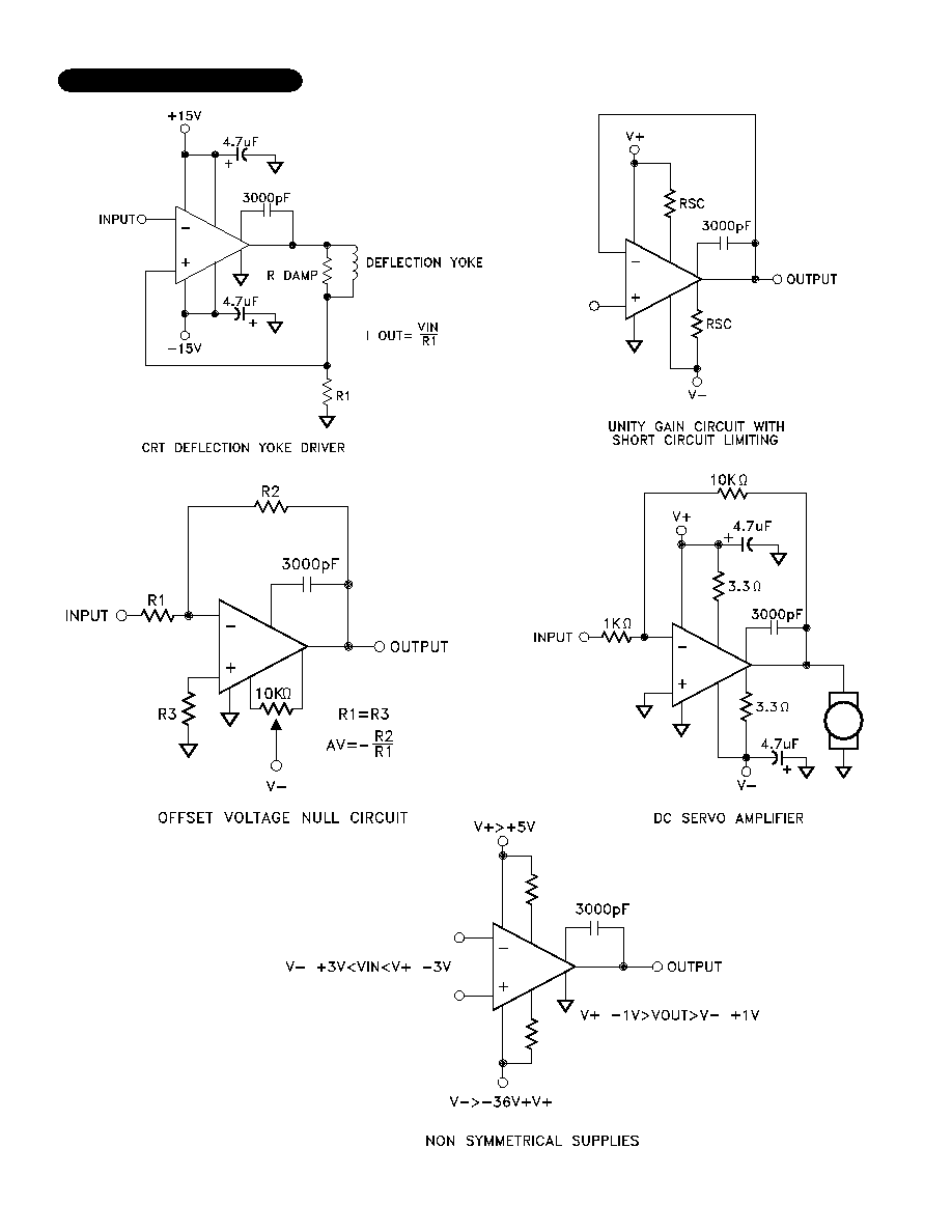
Servo Amplifer
Motor Driver
TYPICAL APPLICATIONS
1 ISC+
2 Compensation
3 GND
4 NC
5 -Input
6 +Input
7 Balance
8 Balance
9 ISC-
10 -VCC
11 Output
12 +VCC
1
PIN-OUT INFORMATION
Rev. - 4/02
ISO 9001 CERTIFIED BY DSCC
FEATURES:
Available as SMD #5962-8508701
Output Current - 0.5 Amps Peak
Low Power Consumption-Class C Design
Programmable Current Limit
High Slew Rate
Continuous Output Short Circuit Duration
Replacement for LH0041
Available in a surface mount package
EQUIVALENT SCHEMATIC
MSK0041
HIGH POWER
OP-AMP
M.S KENNEDY CORP.
0041
SERIES
MEDIUM POWER
OP-AMP
MSK0041FP
DESCRIPTION:
The MSK 0041 and 0041FP are general purpose Class C power operational amplifiers. These amplifiers offer high
output currents, making them an excellent low cost choice for motor drive circuits. The amplifier and load can be pro-
tected from fault conditions through the use of internal current limit circuitry that can be user programmed with two
external resistors. These devices are also compensated with a single external capacitor. The MSK 0041 is available in a
hermetically sealed 12 pin TO-8 package. The MSK 0041FP is packaged in a 12 pin hermetic metal flatpack.
MSK0041 FP
1 GND
2 Balance
3 -Input
4 +Input
5 Balance
6 NC
7 -VCC
8 ISC-
9 Output
10 ISC+
11 +VCC
12 Compensation
Audio Amplifier
Programmable Power Supply
MSK0041
(PIN NUMBERS ARE FOR TO-8)

Group A
Subgroup
-
1, 2, 3
1,2,3
1
2, 3
1
2, 3
1
2,3
-
-
4
5,6
1
2,3
-
4
5,6
4
-
4
4
5,6
4
4
STATIC
Supply Voltage Range
Quiescent Current
Power Consumption
INPUT
Input Capacitance
Input Resistance
Input Noise Voltage
OUTPUT
Settling Time
TRANSFER CHARACTERISTICS
Slew Rate
Transition Times
Overshoot
Max.
±18
±4.0
120
±6.0
-
±500
-
±200
-
-
-
-
-
-
-
-
-
-
300
-
-
-
-
1.5
30
Typ.
±15
±1.0
90
±0.5
-
±150
-
±2.0
-
3
1.0
90
-
95
-
5
±14
-
220
4
3.0
105
-
0.3
5
Min.
±5
-
-
-
-
-
-
-
-
-
0.3
70
-
80
-
-
±13
-
180
-
1.0
100
-
-
-
Max.
±18
±3.5
105
±3.0
±5.0
±300
±1.0
±100
±300
-
-
-
-
-
-
-
-
-
300
-
-
-
-
1.0
20
Typ.
±15
±1.0
75
±0.5
±2.0
±100
±0.4
±2.0
-
3
1.0
90
90
95
-
5
±14
±14
220
4
3.0
105
96
0.3
5
Min.
±5
-
-
-
-
-
-
-
-
-
0.3
70
70
80
80
-
±13
±13
182
-
1.5
100
88
-
-
V
IN
= 0V
V
CM
= 0V
Either Input
F=DC
F=DC
F = 10H
Z
to 10KH
Z
R
SC
= 3.3
V
OUT
= MAX
0.1% 2V step
V
OUT
= ±10V R
L
= 100
V
OUT
=1V Rise and Fall
Small Signal
±V
CC
Supply Voltage
±18V
I
OUT
Peak Output Current 0.5A
V
IN
Differential Input Voltage ±30V
V
IN
Common Mode Input Voltage
±15V
R
TH
Thermal Resistance-Junction to Case
MSK 0041
85∞ C/W
MSK 0041FP 85∞ C/W
ABSOLUTE MAXIMUM RATINGS
ELECTRICAL SPECIFICATIONS
T
ST
Storage Temperature Range -65∞ to +150∞C
T
LD
Lead Temperature Range 300∞C
(10 Seconds)
T
J
Junction Temperature 150∞C
T
C
Case Operating Temperature Range
Military Versions (H/B/E) -55∞C to +125∞C
Industrial Versions -40∞C to +85∞C
Units
V
mA
mW
mV
µV/∞C
nA
µA
nA
nA
pF
M
dB
dB
dB
dB
µV
RMS
V
V
mA
µS
V/µS
dB
dB
µS
%
2
Rev. - 4/02
Military
Industrial
2
Input Bias Current
Output Voltage Swing
R
L
=100
F =100H
Z
Parameter
Test Conditions
4
Input Offset Current
Input Offset Voltage
Power Supply Rejection Ratio
V
CM
= 0V
F = 10H
Z
V
CM
= ±10V
Output Short Circuit Current
Common Mode Rejection Ratio
V
CC
= ±5V to ±15V
Open Loop Voltage Gain
NOTES:
1
Unless otherwise specified, ±V
CC
= ±15V, C
C
= 3000pF.
2
Guaranteed by design but not tested.
Typical parameters are representative of actual device performance but are for reference only.
4
Industrial grade and "E" suffix devices shall be tested to subgroups 1 and 4 unless otherwise specified.
5
Military grade devices (B/H suffix) shall be 100% tested to subgroups 1, 2, 3 and 4.
Subgroup 1, 4
T
A
= T
C
= +25∞C
Subgroup 2, 5
T
A
= T
C
= +125∞C
Subgroup 3, 6
T
A
= T
C
= -55∞C
6
Reference DSCC SMD 5962-8508701 for electrical specifications for devices purchased as such.
7 Subgroup 5 and 6 testing available upon request.
3
2
3
5
2
V
IN
= 0V
3
F = 10H
Z
R
L
= 1K
V
IN
= 0V
3
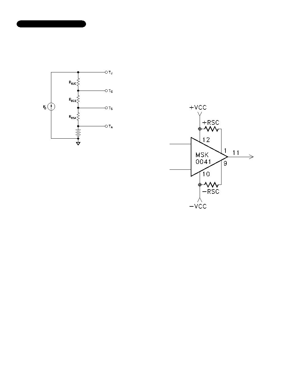
HEAT SINKING
To select the correct heat sink for your application, refer to the
thermal model and governing equation below.
Thermal Model:
APPLICATION NOTES
CURRENT LIMIT
The MSK 0041 has an on-board current limit scheme de-
signed to limit the output drivers anytime output current
exceeds a predetermined limit. The following formula may
be used to determine the value of the current limit resistance
necessary to establish the desired current limit.
Current Limit Connection
3
Rev. - 4/02
R
SC
= 0.7
I
SC
___
See "Application Circuits" in this data sheet for additional
information on current limit connections.
POWER SUPPLY BYPASSING
Both the negative and the positive power supplies must
be effectively decoupled with a high and low frequency by-
pass circuit to avoid power supply induced oscillation. An
effective decoupling scheme consists of a 0.1 microfarad
ceramic capacitor in parallel with a 4.7 microfarad tantalum
capacitor from each power supply pin to ground.This ca-
pacitor will eliminate any peak output voltage clipping which
may occur due to poor power supply load regulation. All
power supply decoupling capacitors should be placed as
close to the package power supply pins as possible.
SAFE OPERATING AREA
The safe operating area curve is a graphical representation
of the power handling capability of the amplifier under vari-
ous conditions. The wire bond current carrying capability,
transistor junction temperature and secondary breakdown
limitations are all incorporated into the safe operating area
curves. All applications should be checked against the curves
to ensure high M.T.B.F.
Governing Equation:
T
J
= P
D
x (R
JC
+ R
CS
+ R
SA
) + T
A
Where
T
J
= Junction Temperature
P
D
= Total Power Dissipation
R
JC
= Junction to Case Thermal Resistance
R
CS
= Case to Heat Sink Thermal Resistance
R
SA
= Heat Sink to Ambient Thermal Resistance
T
C
= Case Temperature
T
A
= Ambient Temperature
T
S
= Sink Temperature
Example:
(TO-8 PACKAGE)
In our example the amplifier application requires the output to drive
a 10 volt peak sine wave across a 100 ohm load for 0.1 amp of
output current. For a worst case analysis we will treat the 0.1 amp
peak output current as a D.C. output current. The power supplies
are ±15 VDC.
1.) Find Power Dissipation
P
D
=[(quiescent current) X (+V
CC
- (V
CC
))] + [(V
S
- V
O
) X I
OUT
]
=(3.5 mA) X (30V) + (5V) X (0.1A)
=0.1W + 0.5W
=0.6W
2.) For conservative design, set T
J
= +150∞C.
3.) For this example, worst case T
A
= +25∞C.
4.) R
JC
= 85∞C/W
5.) Rearrange governing equation to solve for R
SA:
R
SA
= (T
J
- T
A
) / P
D
- (R
JC
) - (R
CS
)
= (150∞C - 25∞C) / 0.6W - (85∞C/W) - (0.15∞C/W)
= 123∞C/W
The heat sink in this example must have a thermal resistance of no
more than 123∞C/W to maintain a junction temperature of less than
+150∞C. This calculation assumes a case to sink thermal resistance
of 0.15∞C/W.
4
Rev. - 4/02
APPLICATION CIRCUITS
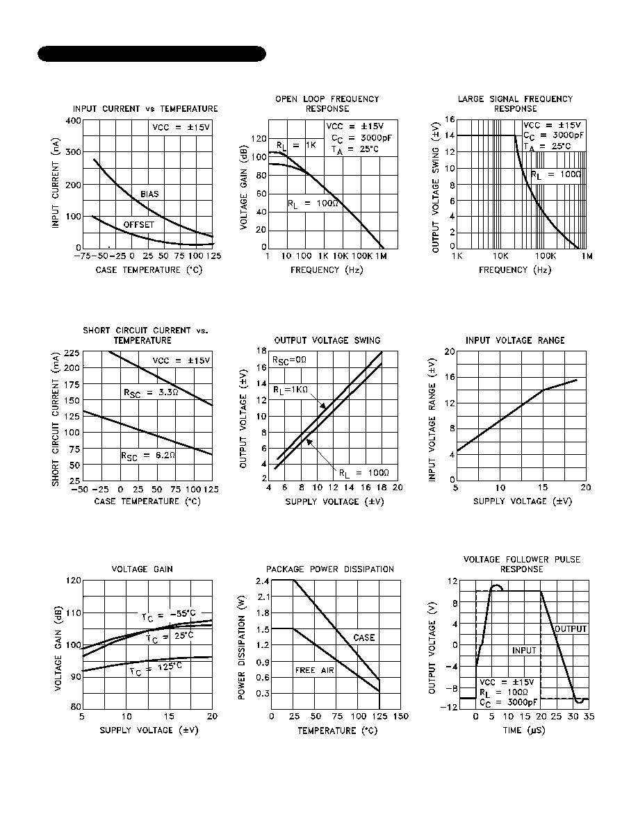
TYPICAL PERFORMANCE CURVES
5
Rev. - 4/02

6
Rev. - 4/02
ORDERING INFORMATION
MECHANICAL SPECIFICATIONS
NOTE: ALL DIMENSIONS ARE ±0.010 INCHES UNLESS OTHERWISE LABELED
MSK0041
Part
Number
MSK 0041 E
MSK 0041
MSK 0041 B
5962-8508701X
Screening Level
Industrial
MIL-PRF-38534 CLASS H
EXTENDED RELIABILITY
DSCC - SMD

7
Rev. - 4/02
M.S. Kennedy Corp.
4707 Dey Road, Liverpool, New York 13088
Phone (315) 701-6751
Fax (315) 701-6752
www.mskennedy.com
The information contained herein is believed to be accurate at the time of printing. MSK reserves the right to make
changes to its products or specifications without notice, however and assumes no liability for the use of its products.
Please visit our website for the most recent revision of this datasheet
MECHANICAL SPECIFICATIONS CONTINUED
NOTE: ALL DIMENSIONS ARE ±0.010 INCHES UNLESS OTHERWISE LABELED.
ESD Triangle indicates pin 1.
ORDERING INFORMATION
DEVICE IS ALSO AVAILABLE WITHOUT LEAD FORMING.
Part
Number
MSK 0041FP E
MSK 0041FP
MSK 0041FP H
Screening Level
Industrial
MIL-PRF-38534 CLASS H
EXTENDED RELIABILITY
DSCC - SMD
TBD
MSK0041FP