 | –≠–ª–µ–∫—Ç—Ä–æ–Ω–Ω—ã–π –∫–æ–º–ø–æ–Ω–µ–Ω—Ç: DAC2812SE | –°–∫–∞—á–∞—Ç—å:  PDF PDF  ZIP ZIP |

4707 Dey Road Liverpool, N.Y. 13088
(315) 701-6751
Wave Solderable Package
All Ceramic Capacitors
Surface Mount Magnetics
MIL STD 461C CR03 (DC-DC Converters)
80 Volt Input Transient Tolerent
Wide Supply Range - 11V to 50V
High Isolation - 500V
High Power Density - 15 W/in≥
Output Voltage Adjustment - Standard
Remote Shutdown
Operates to 11V Input at 5W
Available with 12V or 15V Outputs
See DHC2800S Series for 3.3V and 5.0V Versions
Available Soon to DSCC SMD 5962-93093, 5962-94631,
5962-93094 and 5962-94630
Replaces Interpoint MSA2812S, MSA2815S and
IR ASA2812S, ASA2815S
MIL-PRF-38534 CERTIFIED
ISO-9001 CERTIFIED BY DSCC
M.S.KENNEDY CORP.
5.4W
DC-DC
CONVERTERS
DAC2800S
DESCRIPTION:
Rev. C 7/04
1
SERIES
FEATURES:
The DAC2812S and DAC2815S DC-DC converters are higher output voltage companion devices to MSK's
DHC types. The DAC's provide the ruggedness, reliability and features required to meet the advanced design
challenges of today's hi-rel market. This has been accomplished while retaining a power density of 15 W/
in
3
and 375 mW/gram of power/package performance. The use of advanced substrate and reflow soldering
techniques during construction results in a rugged, cost-effective and completely solderable package.
The DAC2800S hybrid converter series utilizes all ceramic capacitors, surface mount magnetics, and
ultrasonically bonded wires to provide reliable operation at all operating temperatures.
The DAC2800S series standard features include output fault monitoring and/or turn on voltage point
programming via the shutdown pin. All three functions may be implemented simultaneously with a minimum
of external components. An output voltage adjustment / load compensation pin which adjusts outputs
simultaneously is also standard.
Fault tolerant design protects these converters from most external circuit faults. The +output and output
adjust pins will withstand +25 V while the shutdown pin will withstand +50 V, protecting the converters
from a variety of system or board faults; e.g. solder bridges etc. Unique load fault protection circuitry allows
this converter to pull up loads having difficult static load line characteristics and allows short term load
excursions significantly beyond ratings in most applications.
A transformer isolated flyback converter topology operating at a switching frequency of 400 kHz allows
operation over a wide input voltage range. Internal filtering of outputs eliminates the need for external
capacitors in many applications.
The 8-pin package is hermetically sealed and isolated from the internal circuits. Heat sinking is
recommended for full power operation at elevated ambient temperatures.

EQUIVALENT SCHEMATIC
Isolated Step Down Power Supply
Microprocessor Power Source
Low Voltage Subsystem Power Source
TYPICAL APPLICATIONS
1
2
3
4
5
+Output
-Output
NC
Adjust/Comp
Shutdown Plus
PIN-OUT INFORMATION
Case
-Input
+Input
8
7
6
-65∞C to +150∞C
300∞C
See Efficiency Curve
150∞C
5.0∞C/W
ABSOLUTE MAXIMUM RATINGS
+50V
80V
450mA
360mA
-55∞C to +125∞C
-40∞C to +85∞C
Input Voltage (pin 7 to pin 6)
Input Transient (pin 7 to pin 6 @ 50mS)
Output Current
DAC2812S
DAC2815S
Case Temperature Range
DAC2800S H/E
DAC2800S
V
IN
V
INT
I
OUT
T
C
Storage Temperature Range
Lead Temperature Range
(10 Seconds)
Power Dissipation
Junction Temperature
Thermal Resistance
(Switches)
T
ST
T
LD
P
D
T
J
JC
Rev. C 7/04
2
NOTE: Continuous operation at or above the absolute maximum ratings may adversely effect the performance
and/or life of the device.

BW=10KHz to 2MHz
LIN=2µH
V
IN
=16, 28 and 40 VDC
I
OUT
=0, 208 and 417mA
V
IN
=16, 28 and 40 VDC
I
OUT
=0, 208 and 417mA
I
OUT
=208mA to/from 417mA
Transition TIme=30µS
I
OUT
=208mA to/from 417mA
Transition TIme=30µS
V
IN
=16V to/from 40V
Transition Time=30µS
V
IN
=16V to/from 40V
Transition Time=30µS
P
OUT
=5.4W MAX.
P
OUT
=5W MAX.
Enabled, I
OUT
=0mA
Disabled I
OUT
=0mA
No Effect on DC Performance
Input to output or any pin to case @ 500V
R
POT
=50K
11V
V
IN
50V
16V
V
IN
40V
BW=10KHz to 2MHz
1
2
3
4
5
6
7
8
+V
IN
= 28V, I
OUT
= 417mA, T
A
=T
C
=25∞C unless otherwise specified.
Guaranteed by design but not tested. Typical parameters are representative of actual device performance but are for reference only.
Industrial grade and "E" suffix devices shall be tested to subgroups 1 and 4 unless otherwise specified.
Military grade devices ("H" suffix) shall be 100% tested to subgroups 1, 2, 3 and 4.
Subgroups 5 and 6 testing available upon request.
Subgroup 1, 4 T
A
=T
C
=+25∞C
2, 5 T
A
=T
C
=+125∞C
3, 6 T
A
=T
C
= -55∞C
Device has internal shutdown feature that pulses the output with a low duty cycle during faults.
Consult DSCC SMD for electrical parameters for devices purchased as such.
ELECTRICAL SPECIFICATIONS
NOTES:
Rev. C 7/04
3
Capacitive Load
Isolation
Short Circuit Current Limit
Switching Frequency
VOUT Adjustment Range
VDC
VDC
mA
mA
mA
mA
mVrms
mVrms
mAp-p
mAp-p
mV
mV
mV
mV
%
%
mV
mV
µS
µS
mV
mV
µS
µS
mV
mV
mS
mS
µS
µS
mS
V
V
mA
mA
µF
M
A
KHz
%
Min.
11.9
11.76
417
417
450
450
-
-
-
-
-
-
-
-
62
60
-
-
-
-
-
-
-
-
-
-
-
-
-
-
-
16
11
-
-
-
100
0.50
375
±10
Output Voltage
Output Voltage Ripple
Input Current Ripple
Line Regulation
Load Regulation
Efficiency
Step Load Response
Step Load Recovery
Step Line Response
Step Line Recovery
Start Up Overshoot
Start Up Delay
Shutdown Delay
Parameter
Test Conditions
1
Max.
12.1
12.24
-
-
-
-
60
100
125
200
±25
±50
±25
±50
-
-
±500
±700
200
200
±500
±500
200
200
200
200
60
60
500
500
60
40
50
50
2.5
300
-
1.8
425
-
DAC2812S
DAC2812S H/E
Input Voltage Range
Output Current
Units
Typ.
12.0
-
-
-
-
-
15
-
76
-
±5
-
±5
-
67
-
±350
-
80
-
±200
-
90
-
0
-
40
-
250
-
40
-
-
35
1.25
-
-
1.1
400
-
Group A
Subgroup
1
2,3
1
2,3
1
2,3
1
2,3
1
2,3
1
2,3
1
2,3
1
2,3
4
5,6
4
5,6
4
5,6
4
5,6
4
5,6
4
5,6
4
5,6
-
1,2,3
1,2,3
1,2,3
1,2,3
1,2,3
1
1
4
1
7
2
Min.
11.85
-
417
-
450
-
-
-
-
-
-
-
-
-
62
-
-
-
-
-
-
-
-
-
-
-
-
-
-
-
-
16
11
-
-
-
100
0.50
375
±10
Max.
12.15
-
-
-
-
-
60
-
125
-
±30
-
±30
-
-
-
±500
-
200
-
±500
-
200
-
200
-
60
-
500
-
60
40
50
50
2.5
300
-
1.8
425
-
Typ.
12.0
-
-
-
-
-
15
-
76
-
±5
-
±5
-
67
-
±350
-
80
-
±200
-
90
-
0
-
40
-
250
-
40
-
-
35
1.25
-
-
1.1
400
-
Shutdown Recovery
Quiescent Current
2
2
2
2
2
2
DAC2812S
2

BW=10KHz to 2MHz
LIN=2µH
V
IN
=16,28 and 40VDC
I
OUT
=0,167 and 333mA
V
IN
=16,28 and 40VDC
I
OUT
=0,167 and 333mA
I
OUT
=167mA to/from 333mA
Transition TIme=30µS
I
OUT
=167mA to/from 333mA
Transition TIme=30µS
V
IN
=16V to/from 40V
Transition Time=30µS
V
IN
=16V to/from 40V
Transition Time=30µS
P
OUT
=5.4W MAX.
P
OUT
=5W MAX.
Enabled, I
OUT
=0mA
Disabled I
OUT
=0mA
No Effect on DC Performance
Input to output or any pin to case @ 500V
R
POT
=50K
11V
V
IN
50V
16V
V
IN
40V
BW=10KHz to 2MHz
ELECTRICAL SPECIFICATIONS
Rev. C 7/04
4
1
2
3
4
5
6
7
8
+V
IN
= 28V, I
OUT
= 333mA, T
A
=T
C
=25∞C unless otherwise specified.
Guaranteed by design but not tested. Typical parameters are representative of actual device performance but are for reference only.
Industrial grade and "E" suffix devices shall be tested to subgroups 1 and 4 unless otherwise specified.
Military grade devices ("H" suffix) shall be 100% tested to subgroups 1, 2, 3 and 4.
Subgroups 5 and 6 testing available upon request.
Subgroup 1, 4 T
A
=T
C
=+25∞C
2, 5 T
A
=T
C
=+125∞C
3, 6 T
A
=T
C
= -55∞C
Device has internal shutdown feature that pulses the output with a low duty cycle during faults.
Consult DSCC SMD for electrical parameters for devices purchased as such.
NOTES:
Capacitive Load
Isolation
Short Circuit Current Limit
Switching Frequency
VOUT Adjustment Range
VDC
VDC
mA
mA
mA
mA
mVrms
mVrms
mAp-p
mAp-p
mV
mV
mV
mV
%
%
mV
mV
µS
µS
mV
mV
µS
µS
mV
mV
mS
mS
µS
µS
mS
V
V
mA
mA
µF
M
A
KHz
%
Min.
14.90
14.70
333
333
360
360
-
-
-
-
-
-
-
-
63
61
-
-
-
-
-
-
-
-
-
-
-
-
-
-
-
16
11
-
-
-
100
0.40
375
±10
Output Voltage
Output Voltage Ripple
Input Current Ripple
Line Regulation
Load Regulation
Efficiency
Step Load Response
Step Load Recovery
Step Line Response
Step Line Recovery
Start Up Overshoot
Start Up Delay
Shutdown Delay
Parameter
Test Conditions
1
Max.
15.10
15.30
-
-
-
-
60
100
125
200
±25
±50
±25
±50
-
-
±600
±750
200
200
±500
±500
200
200
200
200
60
60
500
500
60
40
50
50
2.5
300
-
1.5
425
-
DAC2815S
DAC2815S H/E
Input Voltage Range
Output Current
Units
Typ.
15.00
15.00
-
-
-
-
15
-
76
-
±5
-
±5
-
68
-
±400
-
100
-
±200
-
90
-
0
0
40
-
250
-
40
-
-
35
1.25
-
-
0.95
400
-
Group A
Subgroup
1
2,3
1
2,3
1
2,3
1
2,3
1
2,3
1
2,3
1
2,3
1
2,3
4
5,6
4
5,6
4
5,6
4
5,6
4
5,6
4
5,6
4
5,6
-
1,2,3
1,2,3
1,2,3
1,2,3
1,2,3
1
1
4
1
7
2
Min.
14.85
-
333
-
360
-
-
-
-
-
-
-
-
-
63
-
-
-
-
-
-
-
-
-
-
-
-
-
-
-
-
16
11
-
-
-
100
0.40
375
±10
Max.
15.15
-
-
-
-
-
60
-
125
-
±30
-
±30
-
-
-
±600
-
200
-
±500
-
200
-
200
-
60
-
500
-
60
40
50
50
2.5
300
-
1.5
425
-
Typ.
12.0
-
-
-
-
-
15
-
76
-
±5
-
±5
-
68
-
±400
-
100
-
±200
-
90
-
0
-
40
-
250
-
40
-
-
35
1.25
-
-
0.95
400
-
Shutdown Recovery
Quiescent Current
2
2
2
2
2
2
DAC2815S
2
APPLICATION NOTES
POWER SUPPLIES
The output voltage of the DAC2812S and DAC2815S may
be adjusted from 90% to 110% of nominal value by the use of
a 150K
potentiometer as shown. Adjustment beyond this
range is possible however certain characteristics of the con-
verter such as but not limited to input voltage range, efficiency,
ripple and temperature performance will change. Characteriza-
tion by the user is recommended in such applications.
Adjust/comp (pin 4) may be driven by external circuitry refer-
enced to pin 2 (-output) if desired. Grounding pin 4 causes
voltage to increase (25% typically) while driving pin 4 above
1.3V causes output voltage to decrease. Pin 4 may be driven
negative without damage, however the resultant increase in
converter output voltage should be considered. Pin 4 may be
driven through 10K
or more if connection of the comp func-
tion is also required.
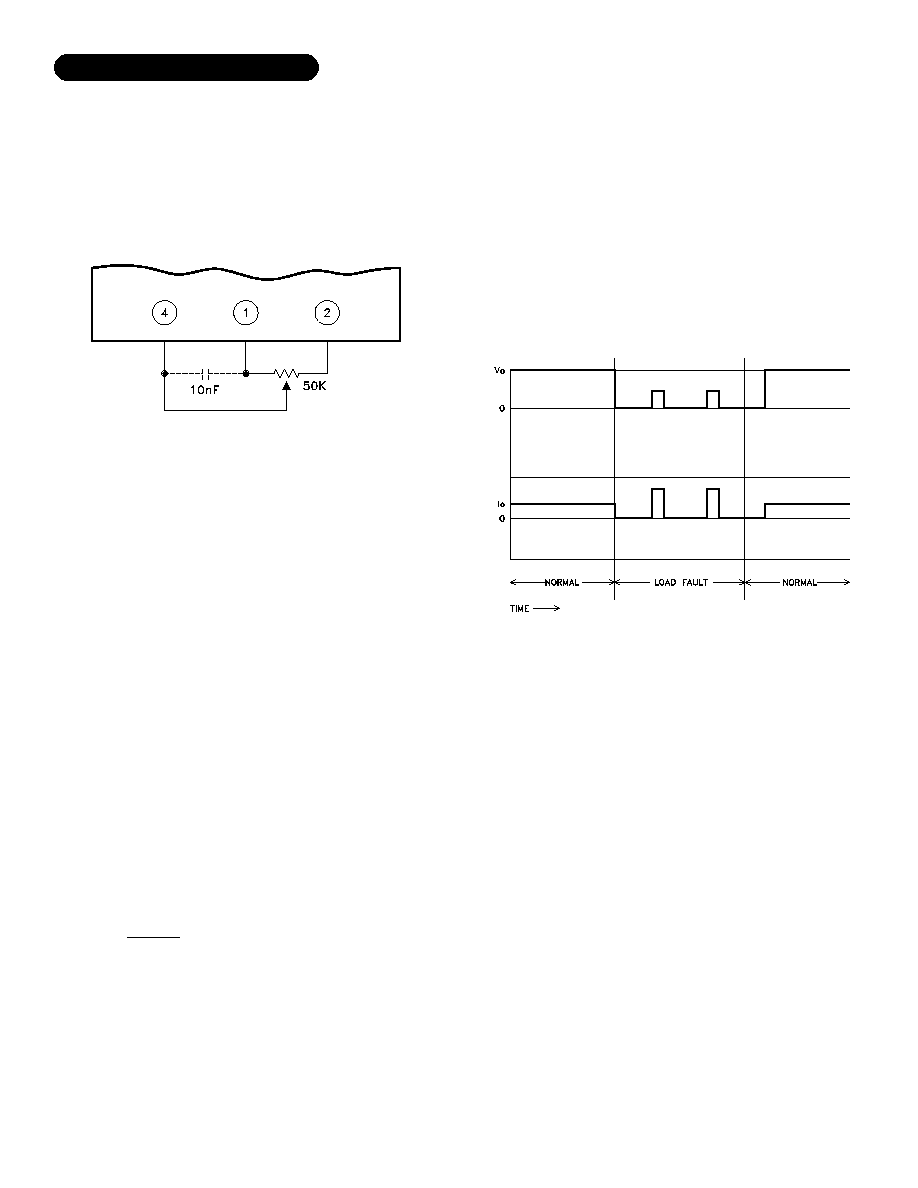
The comp function of pin 4 allows load transient response to
be tailored to suit specific application requirements. This fea-
ture may be utilized by connecting a 10 or less nF capacitor
between pins 4 and 1.
Note: The DAC2812S and DAC2815S use pin 4 while the
DHC2803S and DHC2805S use pin 3.
Rev. C 7/04
5
SHUTDOWN PLUS
Pin 5 is used for remote shutdown, output fault detection,
and/or setting the input voltage point at which the converter
will turn on as shown in the typical application diagram. No
connection to pin 5 is necessary for normal operation of the
converter. Pin 5 is referenced to the pin 7 (-input).
Shutdown may be implemented by simply connecting pin 5
to an open collector logic output or switch rated at 2.5mA,
25Vdc or higher.
Input voltage turn on point is programmed with a single resis-
tor from pin 5 to 7. An input turn on/off hysteresis (typically
3.5% of Vin) will be observed. This should be considered when
making or verifying set point adjustment. The value of the
setpoint resistor may be determined by the following:
R= (±10% accuracy at 25∞C)
Set point temperature coefficient is typically +400ppm/∞C.
Output fault monitoring is accomplished by observing pin 5
with a high impedance monitoring circuit. Pin 5 voltage drops
from over 10V to below 1V when a load fault causes the con-
verters fault protection circuitry to activate. It will remain low
for at least 100mS and return high. If the load fault is still
present pin 5 will return low and the cycle will repeat. A resis-
tor >400K
from pin 5 to 7 provides pull down for pin 5 if
there is no input setpoint programming resistor already in place.
210∑10≥
E
TO
-9.5
LOAD FAULT RESPONSE
The MSK families of DC-DC converters share load fault phi-
losophies. Load fault conditions include short-circuit and se-
vere overload conditions. The DAC2800S converter series re-
sponds to load faults by turning off all power conversion cir-
cuits for 250mS and then attempting to restart for 10mS (typi-
cal). The net "on" duty factor during a fault is very low result-
ing in low converter dissipation and immunity from overheating
at 125∞C. Current beyond rated can flow into the load at
startup time. This allows the converter to bring up capacitive
and other difficult load types more reliably than competing con-
verters.