 | –≠–ª–µ–∫—Ç—Ä–æ–Ω–Ω—ã–π –∫–æ–º–ø–æ–Ω–µ–Ω—Ç: DHD2805SK | –°–∫–∞—á–∞—Ç—å:  PDF PDF  ZIP ZIP |

HI-REL DESIGN
∑ WAVE SOLDERABLE PACKAGE
∑ ALL CERAMIC CAPACITORS
∑ SURFACE MOUNT MAGNETICS
∑ WITHSTANDS 5000G
FEATURES -- SINGLE OUTPUT
∑ REPLACES APEX DHW2805S
∑ NO DERATING -- -55∞C to +125∞C
∑ WIDE SUPPLY RANGE -- 16V to 40V
∑ HIGH ISOLATION -- 500V
∑ HIGH POWER DENSITY -- 17W/IN
3
∑ OUTPUT VOLTAGE ADJUSTMENT --
STANDARD
∑ REMOTE SHUTDOWN
∑ OPERATES TO 11V
IN
AT 5W
∑ AVAILABLE WITH 5V OUTPUT
DESCRIPTION
The DHD2805S DC-DC converter provides the rugged-
ness, reliability, and features required to meet the advanced
design challenges of today's hi-rel market. This is accom-
plished while retaining a power density of 17 W/in
3
and 425
mW/gram of power/package performance. The use of ad-
vanced substrate and reflow soldering techniques during
construction results in a rugged, cost-effective, and com-
pletely solderable package.
DHD2805S hybrid converter series utilizes all ceramic
capacitors and surface mount magnetics to provide reliable
operation at all operating temperatures while surviving very
high G forces.
DHD2805S standard features include output fault monitor-
ing and/or turn on voltage point programming via the shut-
down pin. All three functions may be implemented simulta-
neously with a minimum of external components. An output
voltage adjustment/load compensation pin is also standard.
Fault tolerant design protects these converters from most
external circuit faults. The output and output adjust pins will
withstand +35 V while the shutdown pin will withstand +50 V
protecting the converters from a variety of system or board
faults i.e. solder bridges etc. Unique load fault protection
circuitry allows this converter to pull up loads having difficult
static load line characteristics and allows short term load
excursions significantly beyond ratings in most applications.
A transformer isolated forward converter topology operat-
ing at a switching frequency of 400 KHz allows operation over
a wide input voltage range. Internal filtering of both input and
output eliminates the need for external capacitors in many
applications.
The 8-pin DIP package is hermetically sealed and isolated
from the internal circuits. Heat sinking is recommended for full
power operation at elevated ambient temperatures.
EXTERNAL CONNECTIONS
BLOCK DIAGRAM
P W M
FEED FORWARD
CONTROLLER
ERROR AMPLIFIER
REFERENCE AND
ISOLATION
3
1
2
6
5
7
4707 Dey Road Liverpool, N.Y. 13088
M.S.KENNEDY CORP.
DHD2805S
ISO-9001 CERTIFIED BY DSCC
7.5W
DC-DC
CONVERTER
Rev. - 3/01
1
1
2
3
4
5
+OUTPUT
-OUTPUT
ADJUST/COMP
NO CONNECTION
SHUTDOWN PLUS
8
7
6
CASE
-INPUT
+INPUT
(315) 701-6751
TYPICAL APPLICATION WITH OPTIONS

NOTES:
1.
Unless otherwise stated: T
C
= 25∞C, V
IN
= 28V, I
OUT
= I
OUT
MAX.
2.
Derate power linearly to zero from 125∞C to 135∞C.
3.
Regulation measured between pin 1 and pin 2 1/6" from case.
4.
Recovery spec assumes that converter has been OFF for at least 500ms.
5.
Input voltage can be increased to 12V to 50V at 5W output power.
CAUTION:
The internal substrate contains beryllia (BeO). Do not break the seal. If accidentally broken, do not crush, machine, or
subject to temperatures in excess of 850∞C to avoid generating toxic fumes.
ABSOLUTE MAXIMUM RATINGS
SPECIFICATIONS
DHD2805S
ABSOLUTE MAXIMUM RATINGS
DHD2805S
DHD2805S
DHD2805S
DHD2805S
DHD2805S
INPUT VOLTAGE RANGE (Pin 7 to 6 or 5)
0-50Vdc
INPUT TRANSIENT (Pin 7 to 6)
80V @ 50ms
OUTPUT WITHSTAND (Pin 2 to 1 or 3)
35Vdc
OUTPUT CURRENT (Continuous)
1.2Adc
TEMPERATURE, Storage
≠65∞C, 150∞C
TEMPERATURE, Pin Soldering 10s
300∞C
SPECIFICATIONS
PARAMETER
TEST CONDITIONS
1
MIN
TYP
MAX
UNITS
STEADY STATE
CHARACTERISTICS
INPUT VOLTAGE RANGE
5
16
28
40
Vdc
OUTPUT VOLTAGE
V
IN
; min
max Vdc @ I
MIN
5.00
5.05
5.10
Vdc
OUTPUT CURRENT
V
IN
; min
max Vdc
120
1500
mAdc
EFFICIENCY
62
67
%
OUTPUT RIPPLE VOLTAGE
Bandwidth 10kHz
1MHz
40
80
mVrms
INPUT RIPPLE CURRENT
Bandwidth 10kHz
1MHz
40
100
mArms
OUTPUT POWER
2
0.6
7.5
W
LINE REGULATION
V
IN
; min
max
3
9
25
mVdc
LOAD REGULATION
I
OUT
; min
max
3
15
35
mVdc
TEMPERATURE COEFFICIENT
.006
%/∞C
TEMPERATURE RANGE, case
2
≠55
125
∞C
QUIESCENT CURRENT
I
OUT
= 0A
38
45
mAdc
INHIBITED
Vpin5; < 8Vdc
.09
1.25
2.5
mAdc
ISOLATION CHARACTERISTICS
(input/output/case)
LEAKAGE RESISTANCE
V
TEST
= 500Vdc
100
M
LEAKAGE CAPACITANCE
f = 10kHz
60
pF
DYNAMIC CHARACTERISTICS
LINE STEP RESPONSE
V
IN
; T
R
, T
F
= 10µs
VOLTAGE CHANGE
V
IN
; 16
40 Vdc
300
mV
RECOVERY TIME (95%)
30
µs
LOAD STEP RESPONSE
I
OUT
; T
R
, T
F
= 10µs
VOLTAGE CHANGE
I
OUT
; 50%
max Adc
700
mV
RECOVERY TIME (95%)
40
µs
DYNAMIC CHARACTERISTICS
START-UP OVERSHOOT
V
IN
; 0-50 Vdc
0
400
mV
SHUTDOWN DELAY
V
PIN5
; > 10Vdc
<8Vdc
220
500
µs
SHUTDOWN RECOVERY TIME
4
V
PIN5
; < 8Vdc
> 10Vdc
60
ms
CAUTION
DHD2805S
DHD2805S
DHD2805S
DHD2805S
DHD2805S
PACKAGE THERMAL SPECIFICATIONS
MIN
TYP
MAX
UNITS
RESISTANCE, case to air
30
∞C/W
TEMPERATURE RISE, junction to case
10
15
∞C
Rev. - 3/01
2

TYPICAL PERFORMANCE
GRAPHS
DHD2805S
LINE TRANSIENT RESPONSE
0.0
1.6
OUTPUT CURRENT, I
OUT
(A)
10
12
14
16
LOW LINE DROP OUT
INPUT VOLTAGE, V
IN
(V)
0.4
0.8
1.2
10K
90K
60K
20K
30K 40K
INPUT VOLTAGE, V
IN
(V)
TIME, t (500
µ
sec/DIV)
LOAD TRANSIENT RESPONSE 1000
µ
F
LINE TRANSIENT RESPONSE
EFFICIENCY CONTOURS
11
30
50
40
20
OUTPUT RESPONSE, X (UNITS/DIV)
OUTPUT CURRENT, I
OUT
(A)
.96
.12 .24
.48
.78
1.2
SET POINT RESISTOR, R
SP
(
)
TIME, t (5msec/DIV)
12
16
20
24
28
TURN ON THRESHOLD
TURN ON VOLTAGE, E
TO
(V)
TURN ON RESPONSE
100 200 400
FREQUENCY, f (Hz)
≠100
AUDIO REJECTION
AUDIO REJECTION, A
V
(dB)
0
≠20
≠40
1K 2K
10K 20K
100K
≠60
≠80
RESPONSE, X (UNITS/DIV)
5.0V
0V
0V
28V
V
OUT
V
IN
TEMP = 25
∞
C
TEMP = 25
∞
C
30%
40%
50%
55%
60%
65%
68%
70%
71%
72%
INPUT VOLTAGE, V
IN
(V)
EFFICIENCY CONTOURS
OUTPUT CURRENT, I
OUT
(A)
TEMP =
125
∞
C
30%
40%
50%
55%
60%
63%
66%
68%
69%
70%
INPUT VOLTAGE, V
IN
(V)
EFFICIENCY CONTOURS
11
50
40
20
30
11
50
40
20
30
OUTPUT CURRENT, I
OUT
(A)
.96
.24
.12
.48
.78
1.2
.96
.24
.12
.48
.78
1.2
TEMP = ≠55
∞
C
30%
40%
50%
55%
68%
69%
70%
60%
66%
63%
INCLUDES 1000
µ
F ON OUTPUT BUS
TIME, t (200
µ
sec/DIV)
TIME, t (200
µ
sec/DIV)
TIME, t (200
µ
sec/DIV)
LOAD TRANSIENT RESPONSE 100
µ
F
OUTPUT RESPONSE, X (UNITS/DIV)
OUTPUT RESPONSE, X (UNITS/DIV)
OUTPUT RESPONSE, X (UNITS/DIV)
INCLUDES 100
µ
F ON OUTPUT BUS
INCLUDES 100
µ
F ON OUTPUT BUS
INCLUDES 100
µ
F ON OUTPUT BUS
INCLUDES 100
µ
F ON OUTPUT BUS
TIME, t (100
µ
sec/DIV)
LOAD TRANSIENT RESPONSE
OUTPUT RESPONSE, X (UNITS/DIV)
1.2A
LOAD = 1.2A
LOAD = 1.2A
LOAD = 1.2A
1.2A
600mA
600mA
V
OUT
V
OUT
V
OUT
V
OUT
V
IN
V
IN
11V
16V
600mA
80V
40V
1.2A
V
OUT
I
OUT
I
OUT
I
OUT
1 V
500mA
1 V
500mA
100mV
20V
50mV
10V
1 V
10 V
2
V
500mA
NO OUTPUT BUS CAPCITANCE
V
IN
= 28V
I
OUT
= 1.2A
OUTPUT DC
CURRENT RATING
Rev. - 3/01
3
APPLICATION
INFORMATION
DHD2805S SERIES
3
1
2
50K
10nF
OUTPUT ADJUST / COMP
The output voltage of the DHD2805S may be adjusted
from 90% to 110% of nominal value by the use of a 50K
potentiometer as shown. Adjustment beyond this range is
possible however certain characteristics of the converter such
as but not limited to input voltage range, efficiency, ripple and
temperature performance will change. Characterization by
the user is recommended in such applications.
Adjust/comp (pin 3) may be driven by external circuitry
referenced to pin 2 (-output) if desired. Grounding pin 3 causes
voltage to increase (25% typically) while driving pin 3 above
1.3 V causes output voltage to decrease. Pin 3 may be driven
through 10K
or more if connection of the comp function is
also required.
The comp function of pin 3 allows capacitive loads as large
as 1000 µF to be accommodated on the DHC2805S without
loss of stability. This feature may be utilized by connecting a
10 nF capacitor between pins 3 and 1. This is generally
recommended when low ESR load capacitances of 100 µF or
greater are used.
SHUTDOWN PLUS
Pin 5 is used for remote shutdown, output fault detection,
and/or setting the input voltage point at which the converter
will turn on as shown in the typical application diagram. No
connection to pin 5 is necessary for normal operation of the
converter. Pin 5 is referenced to the ≠input (pin 7).
Shutdown may be implemented by simply connecting pin
5 to an open collector logic output or switch rated at 2.5 mA,
25 Vdc or higher.
Input voltage turn on point is programmed with a single
resistor from pin 5 to 7. An input turn on/off hysteresis (typically
3.5% of Vin) will be observed. This should be considered when
making or verifying set point adjustment. The value of the
setpoint resistor may be determined by the following:
210 ∑ 10
3
R =
(±10% accuracy at 25∞C)
E
TO
≠ 9.5
Set point temperature coefficient is typically +400ppm/∞C.
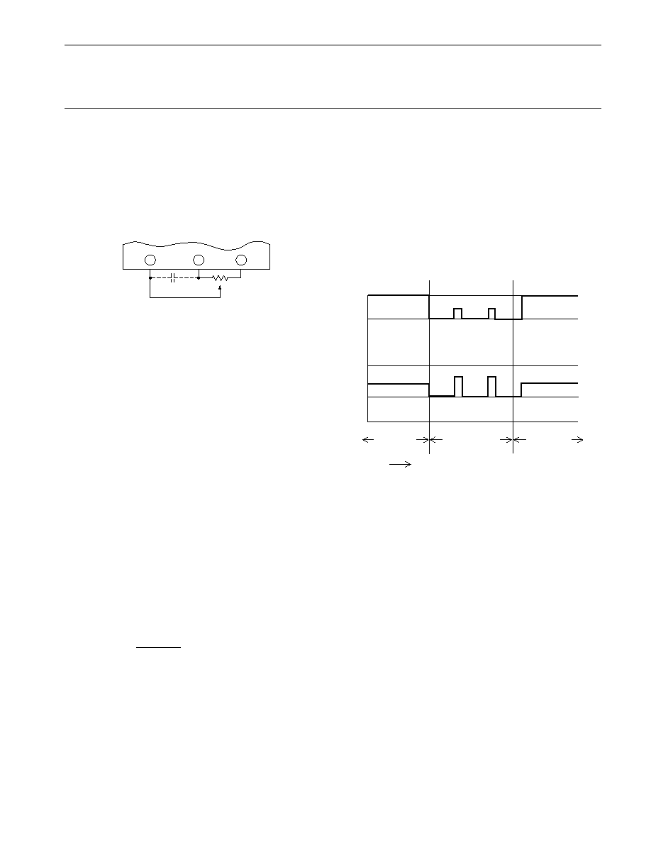
Output fault monitoring is accomplished by observing pin
5 with a high impedance monitoring circuit. Pin 5 voltage drops
from over 10 V to below 1 V when a load fault causes the
converters fault protection circuitry to activate. It will remain
low for at least 100 ms and return high. If the load fault is still
present pin 5 will return low and the cycle will repeat. A resistor
> 400 K
from pin 5 to 7 provides pull down for pin 5 if there
is no input setpoint programming resistor already in place.
Vo
NORMAL
TIME
NORMAL
LOAD FAULT
O
I
o
O
LOAD FAULT RESPONSE
Load fault conditions include short-circuit and severe over-
load conditions. The DHC2800 converter series responds to
load faults by turning off all power conversion circuits for 250
mS and then attempting to restart for 10 mS (typical). The net
"on" duty factor during a fault is very low resulting in low
converter dissipation and immunity from overheating at 125∞C.
Current beyond rated can flow into the load at startup time.
This allows the converter to bring up capacitive and other
difficult load types more reliably than competing converters.
Rev. - 3/01
4
The information contained herein is believed to be accurate at the time of printing. MSK reserves the right to make
changes to its products or specifications without notice, however, and assumes no liability for the use of its products.
Please visit our website for the most recent revision of this datasheet.
M.S. Kennedy Corp.
4707 Dey Road, Liverpool, New York 13088
Phone (315) 701-6751
FAX (315) 701-6752
www.mskennedy.com
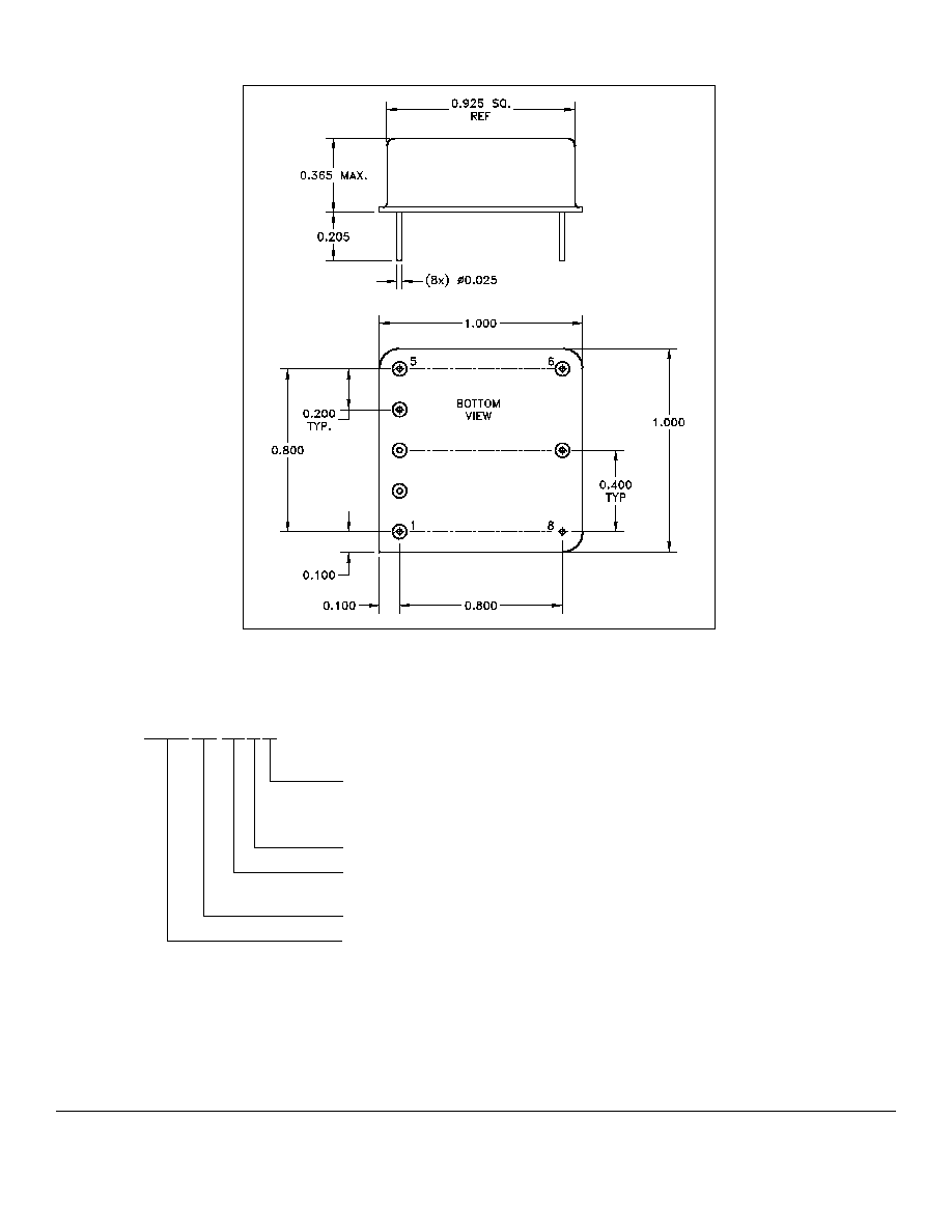
NOTE: ALL DIMENSIONS ARE ±0.010 INCHES UNLESS OTHERWISE LABELED.
ESD Triangle indicates Pin 1.
DHD2805S
The above example is an industrial grade 5V single output converter
ORDERING INFORMATION
SCREENING
BLANK= INDUSTRIAL; E= EXTENDED RELIABILITY;
H= CLASS H; K= CLASS K
SINGLE OUTPUT
OUTPUT VOLTAGE
05=5V
NOMINAL INPUT VOLTAGE
GENERAL PART NUMBER
Rev. - 3/01
5
MECHANICAL SPECIFICATIONS