PROTECTION PRODUCTS
1
www.semtech.com
PRELIMINARY
PROTECTION PRODUCTS - EMIClamp
TM
EClamp2340C
EMI Filter and ESD Protection
for Color LCD Interface
Description
Features
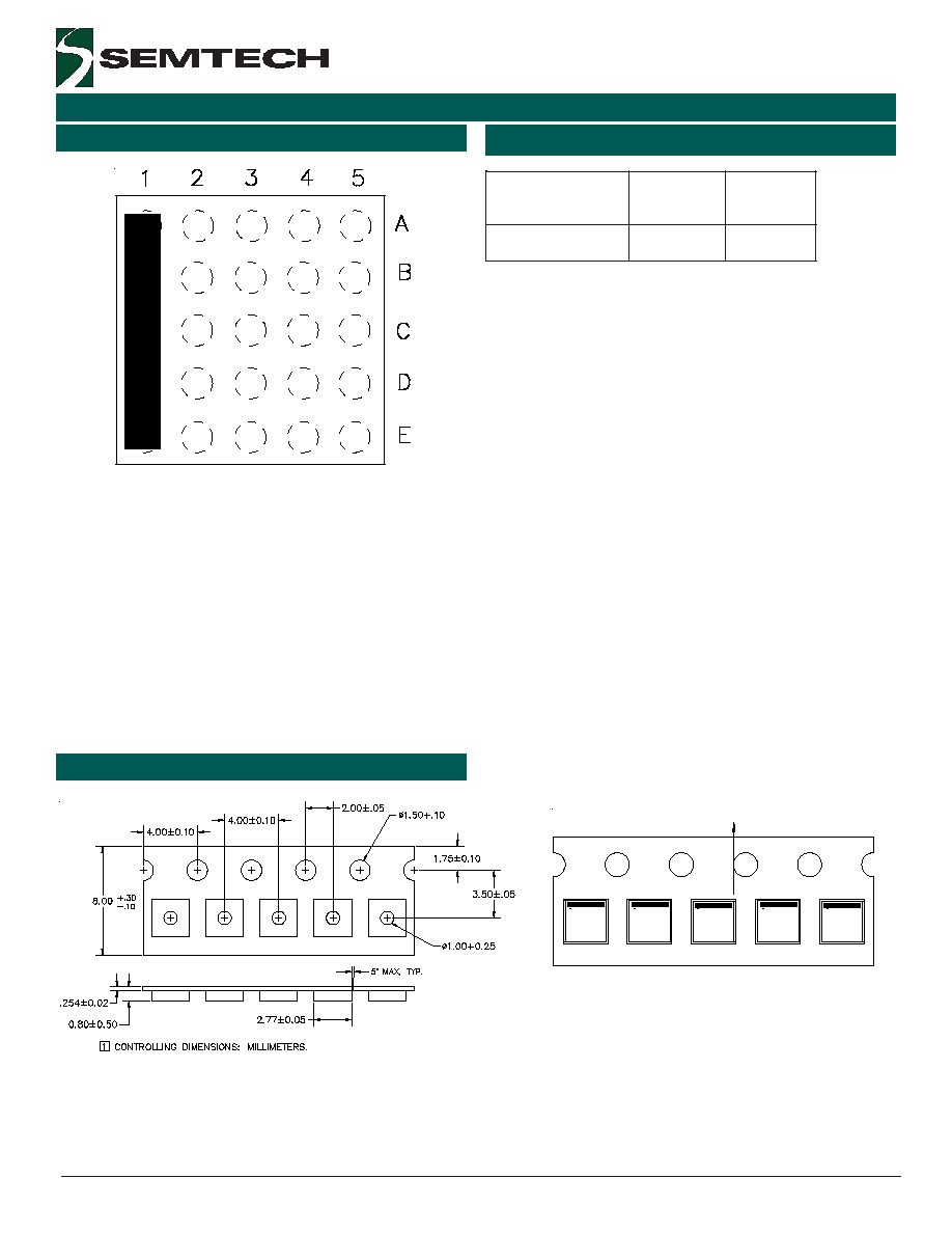
PIN Configuration
Revision 4/19/2004
5 x 5 Grid Flip Chip (Ball Side View)
The EClamp
TM
2340C is a low pass filter array with
integrated TVS diodes. It is designed to suppress
unwanted EMI/RFI signals and provide electrostatic
discharge (ESD) protection in portable electronic
equipment. This state-of-the-art device utilizes solid-
state silicon-avalanche technology for superior clamp-
ing performance and DC electrical characteristics.
They have been optimized for protection of color
protection of color
protection of color
protection of color
protection of color
LCD panels
LCD panels
LCD panels
LCD panels
LCD panels in cellular phones and other portable
electronics.
The device consists of ten identical circuits comprised
of TVS diodes for ESD protection, and a resistor -
capacitor network for EMI/RFI filtering. A series
resistor value of 100
and a capacitance value of
18pF is used to achieve 20dB minimum attenuation
from 800MHz to 3GHz. Each line features two stages
of TVS diode protection. The TVS diodes provide
effective suppression of ESD voltages in excess of
15kV (air discharge) and 8kV (contact discharge) per
IEC 61000-4-2, level 4.
The device is a 25-bump, 0.5mm pitch flip chip array
with a 5x5 bump grid. It measures 2.6 x 2.6 x
0.65mm. The solder bumps have a nominal diameter
of 0.315mm.
Mechanical Characteristics
Circuit Diagram
Applications
Color LCD Panel Protection
Cell Phone CCD Camera Lines
Personal Digital Assistants (PDA's)
JEDEC MO-211, Variation BF, 0.50 mm pitch flip
chip
Nominal Dimensions: 2.6 x 2.6 x 0.65 mm
Bump Diameter: 315+/-20
�
m
Non-conductive top side coating
Marking : Mark code, lot code, orientation mark
Packaging : Tape and Reel per EIA 481
Flip Chip bidirectional EMI/RFI filter with
integrated ESD protection
ESD protection to IEC 61000-4-2 (ESD) Level4,
+/-15kV (air), +/-8kV (contact)
Filter performance: 20dB minimum attenuation
800MHz to 3GHz
TVS working voltage: 5V
Resistor: 100 Ohms
Input Capacitance: 18pF (VR = 2.5V
DC
)
Protection and filtering for ten lines
Solid-state technology
Circuit 10x
LOW PASS FILTER
C
IN
= 18pF
R = 100 Ohms
2
2004 Semtech Corp.
www.semtech.com
PRELIMINARY
PROTECTION PRODUCTS - EMIClamp
TM
EClamp2340C
Absolute Maximum Rating
Electrical Characteristics (T=25
o
C)
g
n
i
t
a
R
l
o
b
m
y
S
e
u
l
a
V
s
t
i
n
U
)
r
i
A
(
2
-
4
-
0
0
0
1
6
C
E
I
r
e
p
D
S
E
)
t
c
a
t
n
o
C
(
2
-
4
-
0
0
0
1
6
C
E
I
r
e
p
D
S
E
V
D
S
E
5
1
-
/
+
5
1
-
/
+
V
k
e
r
u
t
a
r
e
p
m
e
T
n
o
it
c
n
u
J
T
J
5
2
1
o
C
e
r
u
t
a
r
e
p
m
e
T
g
n
it
a
r
e
p
O
T
p
o
5
8
+
o
t
0
4
-
o
C
e
r
u
t
a
r
e
p
m
e
T
e
g
a
r
o
t
S
T
G
T
S
0
5
1
+
o
t
5
5
-
o
C
r
e
t
e
m
a
r
a
P
r
e
t
e
m
a
r
a
P
r
e
t
e
m
a
r
a
P
r
e
t
e
m
a
r
a
P
r
e
t
e
m
a
r
a
P
l
o
b
m
y
S
l
o
b
m
y
S
l
o
b
m
y
S
l
o
b
m
y
S
l
o
b
m
y
S
s
n
o
i
t
i
d
n
o
C
s
n
o
i
t
i
d
n
o
C
s
n
o
i
t
i
d
n
o
C
s
n
o
i
t
i
d
n
o
C
s
n
o
i
t
i
d
n
o
C
m
u
m
i
n
i
M
m
u
m
i
n
i
M
m
u
m
i
n
i
M
m
u
m
i
n
i
M
m
u
m
i
n
i
M
l
a
c
i
p
y
T
l
a
c
i
p
y
T
l
a
c
i
p
y
T
l
a
c
i
p
y
T
l
a
c
i
p
y
T
m
u
m
i
x
a
M
m
u
m
i
x
a
M
m
u
m
i
x
a
M
m
u
m
i
x
a
M
m
u
m
i
x
a
M
s
t
i
n
U
s
t
i
n
U
s
t
i
n
U
s
t
i
n
U
s
t
i
n
U
e
g
a
tl
o
V
f
f
O
-
d
n
a
t
S
e
s
r
e
v
e
R
S
V
T
V
M
W
R
5
V
e
g
a
tl
o
V
n
w
o
d
k
a
e
r
B
e
s
r
e
v
e
R
S
V
T
V
R
B
I
t
A
m
1
=
6
8
0
1
V
t
n
e
r
r
u
C
e
g
a
k
a
e
L
e
s
r
e
v
e
R
S
V
T
I
R
V
M
W
R
V
0
.
3
=
5
.
0
A
�
e
c
n
a
t
s
i
s
e
R
s
e
ir
e
S
l
a
t
o
T
R
e
n
i
L
h
c
a
E
5
8
0
0
1
5
1
1
s
m
h
O
e
c
n
a
ti
c
a
p
a
C
l
a
t
o
T
C
n
i
,
d
n
u
o
r
G
o
t
t
u
p
n
I
e
n
i
L
h
c
a
E
V
R
z
H
M
1
=
f
,
V
0
=
7
2
F
p
e
c
n
a
ti
c
a
p
a
C
l
a
t
o
T
C
n
i
,
d
n
u
o
r
G
o
t
t
u
p
n
I
e
n
i
L
h
c
a
E
V
R
z
H
M
1
=
f
,
V
5
.
2
=
8
1
F
p

3
2004 Semtech Corp.
www.semtech.com
PRELIMINARY
PROTECTION PRODUCTS - EMIClamp
TM
EClamp2340C
Typical Characteristics
Typical Insertion Loss S21 (Each Line)
Analog Crosstalk (Each Line)
ESD Clamping (+8kV Contact)
START . 030 MHz
3
STOP 000 . 000 000 MHz
CH1 S21 LOG
6 dB / REF 0 dB
START . 030 MHz
3
STOP 000 . 000 000 MHz
CH1 S21 LOG
20 dB / REF 0 dB
Series Resistance vs. Temperature
ESD Clamping (-8kV Contact)
Capacitance vs. Reverse Voltage
(Normalized to 2.5 volts)
90.0
95.0
100.0
105.0
-40
-30
-20
-10
0
10
20
30
40
50
60
70
80
Temperature (
o
C)
Ser
i
e
s
R
esistance
(Oh
m
)
0
0.2
0.4
0.6
0.8
1
1.2
1.4
1.6
0
0.5
1
1.5
2
2.5
3
3.5
4
4.5
5
Reverse Voltage - VR (V)
Normalized Capacitance
4
2004 Semtech Corp.
www.semtech.com
PRELIMINARY
PROTECTION PRODUCTS - EMIClamp
TM
EClamp2340C
Applications Information
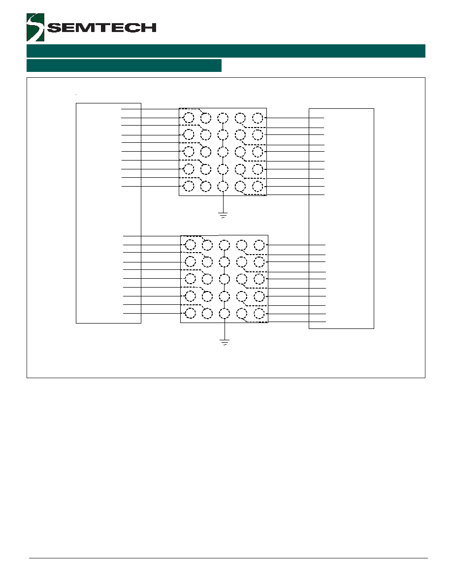
Device Connection Options
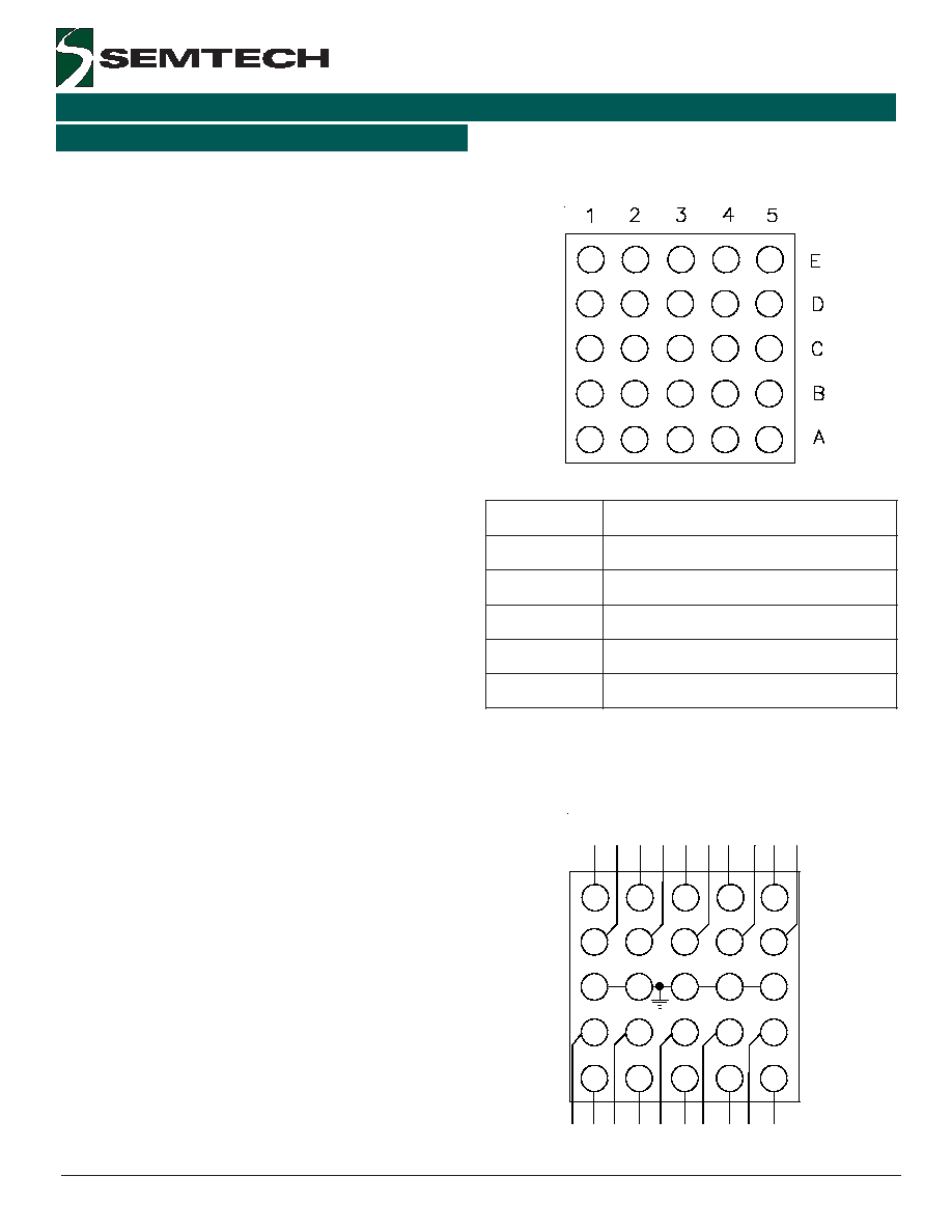
The EClamp2340C has solder bumps located in a 5 x 5
matrix layout on the active side of the device. The
bumps are designated by the numbers 1 - 5 along the
horizontal axis and letters A - E along the vertical axis.
The input of the lines to be protected are connected at
bumps A1 - A5 and B1 - B5. The line outputs are
connected at bumps D1 - D5 and E1 - E5. Bumps C1 -
C5 are connected to ground. All path lengths should
be kept as short as possible to minimize the effects of
parasitic inductance in the board traces.
Wafer Level CSP TVS
CSP TVS devices are wafer level chip scale packages.
They eliminate external plastic packages and leads and
thus result in a significant board space savings. Manu-
facturing costs are minimized since they do not require
an intermediate level interconnect or interposer layer
for reliable operation. They are compatible with cur-
rent pick and place equipment further reducing manu-
facturing costs. Certain precautions and design
considerations have to be observed however for
maximum solder joint reliability. These include solder
pad definition, board finish, and assembly parameters.
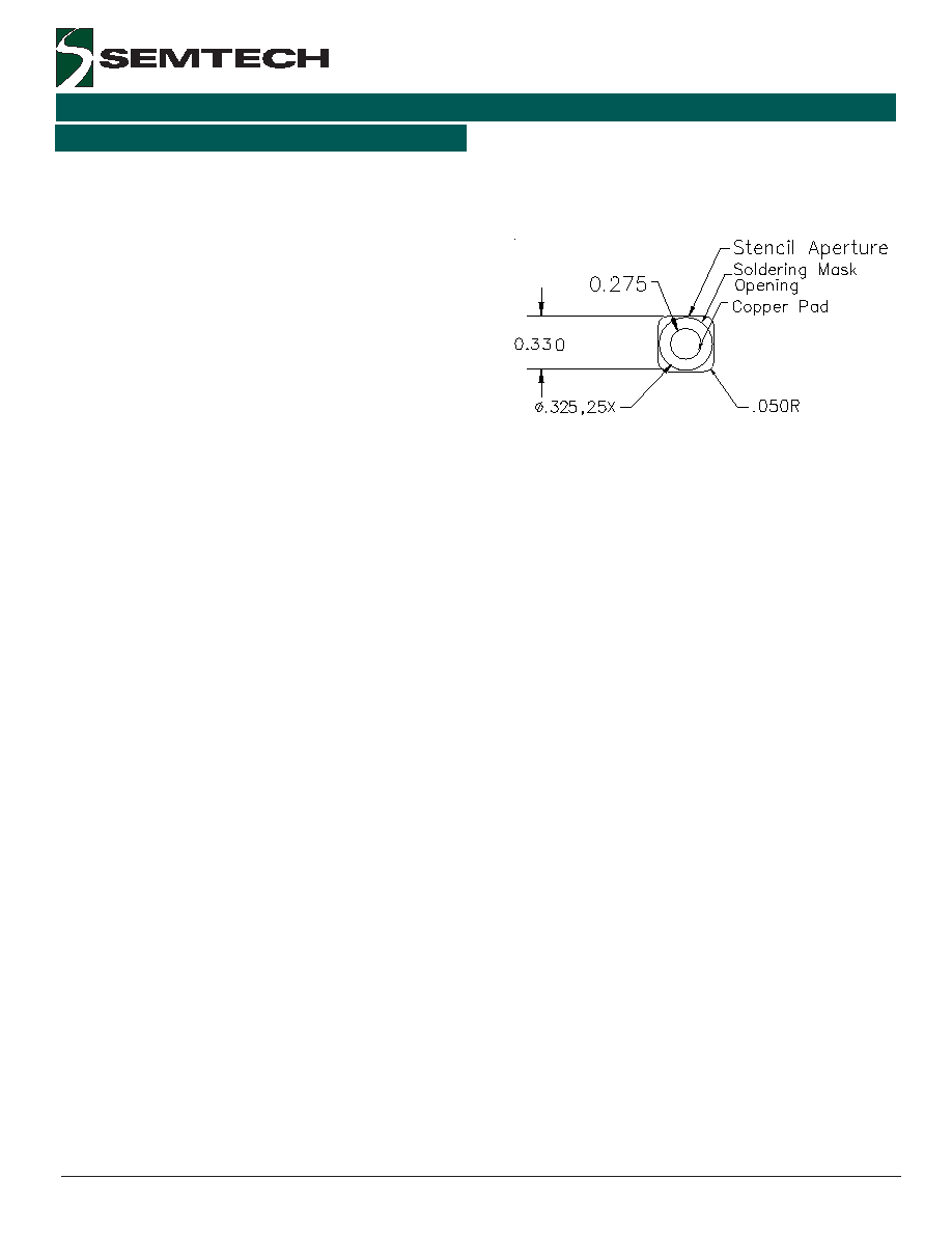
Printed Circuit Board Mounting
Non-solder mask defined (NSMD) land patterns are
recommended for mounting flip chip devices. Solder
mask defined (SMD) pads produce stress points at the
solder mask to solder ball interface that can result in
solder joint cracking when exposed to extreme fatigue
conditions. The recommended pad size is 0.275 �
0.010 mm with a minimum solder mask opening of
0.325 mm.
Grid Courtyard
The recommended grid placement courtyard is 2.7 x
2.7 mm. The grid courtyard is intended to encompass
the land pattern and the component body that is
centered in the land pattern. When placing parts on a
PCB, the highest recommended density is when one
courtyard touches another.
Pin Identification and Configuration (Ball Side View)
n
i
P
n
o
i
t
a
c
i
f
i
t
n
e
d
I
5
A
-
1
A
5
,
4
,
3
,
2
,
1
s
e
n
i
L
,t
u
p
n
I
5
B
-
1
B
0
1
,
9
,
8
,
7
,
6
s
e
n
i
L
,t
u
p
n
I
5
C
-
1
C
d
n
u
o
r
G
5
D
-
1
D
0
1
,
9
,
8
,
7
,
6
s
e
n
i
L
,t
u
p
t
u
O
5
E
-
1
E
5
,
4
,
3
,
2
,
1
s
e
n
i
L
,t
u
p
t
u
O
Layout Example (Ball Side View)
1
6
2
7
3
8
4
9
5
10
6
1
7
2
8
3
9
4 10
5
Output
Input
5
2004 Semtech Corp.
www.semtech.com
PRELIMINARY
PROTECTION PRODUCTS - EMIClamp
TM
EClamp2340C
Applications Information
Recommended NSMD Pad and Stencil Aperture
Printed Circuit Board Finish
A uniform board finish is critical for good assembly
yield. Two finishes that provide uniform surface coat-
ings are immersion nickel gold and organic surface
protectant (OSP). A non-uniform finish such as hot air
solder leveling (HASL) can lead to mounting problems
and should be avoided.
Stencil Design
A properly designed stencil is key to achieving ad-
equate solder volume without compromising assembly
yields. A 0.100mm to 0.200mm thick, laser cut,
electro-polished stencil with 0.330mm apertures
corners with rounded corners is recommended.
Reflow Profile
The flip chip TVS can be assembled using the reflow
requirements for IPC/JEDEC standard J-STD-020B for
Sn-Pb eutectic assembly of small body components.
During reflow, the component will self-align itself on the
pad.
Circuit Board Layout Recommendations for Suppres-
sion of ESD
Good circuit board layout is critical for the suppression
of ESD induced transients. The following guidelines are
recommended:
Place the TVS near the input terminals or connec-
tors to restrict transient coupling.
Minimize the path length between the TVS and the
protected line.
Minimize all conductive loops including power and
ground loops.
The ESD transient return path to ground should be
kept as short as possible.
Never run critical signals near board edges.
Use ground planes whenever possible.
6
2004 Semtech Corp.
www.semtech.com
PRELIMINARY
PROTECTION PRODUCTS - EMIClamp
TM
EClamp2340C
Applications Information
Implementation Example
1
6
2
7
3
8
4
9
5
10
6
1
7
2
8
3
9
4
10
5
B
a
s
e
b
an
d
C
o
n
t
ro
ll
er
LC
D Disp
la
y
1
6
2
7
3
8
4
9
5
10
6
1
7
2
8
3
9
4
10
5
EClamp2340C
EClamp2340C
1
6
2
7
3
8
4
9
5
10
6
1
7
2
8
3
9
4
10
5
1
6
2
7
3
8
4
9
5
10
6
1
7
2
8
3
9
4
10
5
1
6
2
7
3
8
4
9
5
10
6
1
7
2
8
3
9
4
10
5
B
a
s
e
b
an
d
C
o
n
t
ro
ll
er
LC
D Disp
la
y
1
6
2
7
3
8
4
9
5
10
6
1
7
2
8
3
9
4
10
5
1
6
2
7
3
8
4
9
5
10
6
1
7
2
8
3
9
4
10
5
1
6
2
7
3
8
4
9
5
10
6
1
7
2
8
3
9
4
10
5
EClamp2340C
EClamp2340C

7
2004 Semtech Corp.
www.semtech.com
PRELIMINARY
PROTECTION PRODUCTS - EMIClamp
TM
EClamp2340C
Applications Information
Insertion Loss Measurement Conditions
Insertion Loss
The insertion loss of the device is the ratio of the
power delivered to the load with and without the filter
in the circuit. This parameter is dependent upon the
impedance of the source and the load. The standard
impedance of test equipment that is used to measure
filter frequency response is 50
.
In order to obtain an
accurate measurement of the filter performance, an
evaluation board with 50
transmission lines are
used. The test conditions for the EClamp2340C are
shown below. The evaluation board contains SMA
connectors at each of the circuits inputs and outputs.
The connections are made with 50
traces. An HP
8753E network analyzer with an internal spectrum
analyzer and tracking generator is used. This equip-
ment has the capability to sweep the device from 3kHz
to 3GHz. The analyzer's source (R
S
) impedance is
equal to the load (R
L
) impedance which is equal to
50
.
Insertion Loss S21
50 Ohms
To Connector
(Output)
To Connector
(Input)
50 Ohms
Vg
START . 030 MHz
3
STOP 000 . 000 000 MHz
CH1 S21 LOG
6 dB / REF 0 dB

8
2004 Semtech Corp.
www.semtech.com
PRELIMINARY
PROTECTION PRODUCTS - EMIClamp
TM
EClamp2340C
Land Pattern
Outline Drawing
0.275
0.5
0.5
9
2004 Semtech Corp.
www.semtech.com
PRELIMINARY
PROTECTION PRODUCTS - EMIClamp
TM
EClamp2340C
Marking
Top View Showing Laser Mark
Tape and Reel Specification
Tape Specifications
Device Orientation in Tape
TT
TT
Top Coating:
op Coating:
op Coating:
op Coating:
op Coating: The top (non-bump side) of the device
is coated with 50 - 90�m of white, non-conductive
coating. The coating is laser markable and helps
prevent die chipping during the PCB assembly process.
This material is compliant with UL 94V-0 flammability
requirements.
Ordering Information
r
e
b
m
u
N
t
r
a
P
r
e
p
y
t
Q
l
e
e
R
e
z
i
S
l
e
e
R
C
W
.
C
0
4
3
2
p
m
a
l
C
E
0
0
0
3
h
c
n
I
7
2340
xxxxxxx-xx
C
Note: xxxxxxx-xx = Wafer Lot Code
Pin A1
2340
C
xx
xxx
xx
-xx
2340
C
xx
xxx
xx
-xx
2340
C
xx
xxx
xx
-xx
2340
C
xx
xxx
xx
-xx
2340
C
xx
xxx
xx
-xx

10
2004 Semtech Corp.
www.semtech.com
PRELIMINARY
PROTECTION PRODUCTS - EMIClamp
TM
EClamp2340C
Contact Information
Semtech Corporation
Protection Products Division
200 Flynn Rd., Camarillo, CA 93012
Phone: (805)498-2111 FAX (805)498-3804