TYPICAL APPLICATIONS
4707 Dey Road Liverpool, N.Y. 13088
(315) 701-6751
MIL-PRF-38534 QUALIFIED
0024
ISO-9001 CERTIFIED BY DSCC
M.S.KENNEDY CORP.
FEATURES:
High Speed DAC Buffer
High Speed Flash ADC Buffer
High Speed Cable Driver
Imaging Equipment
HIGH SPEED
OPERATIONAL AMPLIFIER
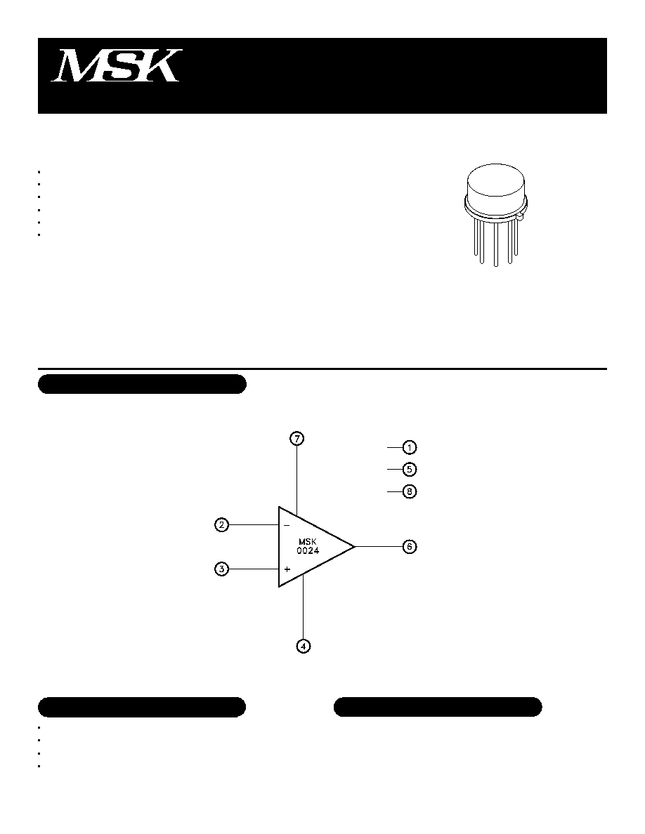
EQUIVALENT SCHEMATIC
TYPICAL APPLICATIONS
DESCRIPTION:
The MSK 0024 is a wide bandwidth, high slew rate operational amplifier ideally suited for use as a buffer to A to
D and D to A converters and high speed comparators. The device is internally compensated and will remain stable
when driving a capacitive load. The MSK 0024 is also a pin similar replacement for the popular LH0024. The MSK
0024 is internally compensated and can replace the LH0024 in most applications without any changes to existing
circuitry. The device is packaged in a hermetically sealed 8 pin metal can.
PIN-OUT INFORMATION
NC
-Input
+Input
-V
CC
Pin Similar Replacement for LH0024
High Slew Rate: 400V/µS Typ.
Fast Settling Time
Excellent DC Performance
Excellent Video Specifications
Internally Compensated for Unity Gain Operation
1
2
3
4
Rev. A 3/03
1
NC
+V
CC
Output
NC
8
7
6
5

STATIC
Supply Voltage Range
Quiescent Current
INPUT
Input Offset Voltage
Input Offset Voltage Drift
Input Bias Current
Input Offset Current
Common Mode Rejection Ratio
Input Impedence
Input Capacitance
OUTPUT
Output Voltage Swing
Power Bandwidth
TRANSFER CHARACTERISTICS
Slew Rate
Open Loop Voltage Gain
Thermal Resistance
Storage Temperature Range
Lead Temperature Range
(10 Seconds)
Junction Temperature
ABSOLUTE MAXIMUM RATINGS
±18V
600mW
±V
CC
±15V
6V
-55∞C to +125∞C
-40∞C to +85∞C
Supply Voltage
Internal Power Dissipation
Input Voltage
Differential Input Voltage
Case Operating Temperature Range
MSK0024H/E
MSK0024
-65∞C to +150∞C
300∞C
175∞C
1
2
3
4
5
6
T
ST
T
LD
T
J
V
CC
P
D
V
IN
V
IND
T
C
Unless otherwise specified, V
CC
=±15V
DC
and V
IN
=0V.
Guaranteed by design but not tested. Typical parameters are representative of actual device performance but are for reference only.
Industrial grade and "E" suffix devices shall be tested to subgroups 1 and 4 unless otherwise requested.
Military grade devices ("H" suffix) shall be 100% tested to subgroups 1,2,3 and 4.
Subgroup 5 and 6 testing available upon request.
Subgroup 1,4 T
C
=+25∞C
Subgroup 2,5 T
C
=+125∞C
Subgroup 3,6 T
A
=-55∞C
NOTES:
Group A
Subgroup
-
1
2,3
1
2,3
-
1
2,3
1
2,3
1
-
-
4
-
4
4
-
AV=5 RS=50
V
CM
=0V
V
CM
=0V
V
CM
=±10V
DC
-V
CC
=-15V +V
CC
=+5V to +15V
+V
CC
=+15V -V
CC
=-5V to -15V
R
L
=2K
V
OUT
=±10V
PK
R
L
=2K
V
OUT
=±10V
PK
R
L
=2K
V
OUT
=±10V
PK
f=10H
Z
Junction to Case @ 125∞C
Typ.
±15
±6
±6
±0.5
±1.0
±15
±4
±5
±1
±1
95
300
1.5
±12.5
4.5
400
8
50
Test Conditions
Max.
±18
±15
±15
±3.0
±5.0
-
±20
±30
±5
±5
-
-
-
-
-
-
-
58
Min.
±5
-
-
-
-
-
-
-
-
-
75
-
-
±12.0
-
220
3
-
Min.
±5
-
-
-
-
-
-
-
-
-
75
-
-
±12.0
-
200
3
-
Max.
±18
±18
-
±4.0
-
-
±30
-
±10
-
-
-
-
-
-
-
-
65
Typ.
±15
±6
-
±0.5
-
±15
±4
-
±1
-
95
300
1.5
±12.5
4.5
400
8
50
V
mA
mA
mV
mV
µV/∞C
µA
µA
µA
µA
dB
K
pF
V
MHz
V/µS
V/mV
∞C/W
MSK0024H/E
MSK0024
Parameter
ELECTRICAL SPECIFICATIONS
2
Rev. A 3/03
Units
Power Supply Rejection Ratio
75
95
-
75
95
dB
1
-
2
2
2
2
2
2
2
2
2
2

APPLICATION NOTES
3
Rev. A 3/03
HEAT SINKING
To determine if a heat sink is necessary for your appli-
cation and if so, what type, refer to the thermal model
and governing equation below.
Thermal Model:
Governing Equation:
T
J
=
P
D
X (R
JC
+ R
CS
+ R
SA
) + T
A
Where
T
J
= Junction Temperature
P
D
= Total Power Dissipation
R
JC
= Junction to Case Thermal Resistance
R
CS
= Case to Heat Sink Thermal Resistance
R
SA
= Heat Sink to Ambient Thermal Resistance
T
C
= Case Temperature
T
A
= Ambient Temperature
T
S
= Sink Temperature
Example:
The example demonstrates a worst case analysis for
the op-amp output stage. This occurs when the output
voltage is 1/2 the power supply voltage. Under this con-
dition, maximum power transfer occurs and the output
is under maximum stress.
Conditions:
V
CC
=±16VDC
V
OUT
=±8Vp Sine Wave, Freq.=1KHz
R
L
=200
For a worst case analysis we treat the +8Vp sine wave
as an 8 VDC output voltage.
1.) Find driver power dissipation
P
D
=(V
CC
-V
OUT
) (V
OUT
/R
L
)
=(16V-8V) (8V/200
)
=320mW
2.) For conservative design, set T
J
=+125∞C.
3.) For this example, worst case T
A
=+100∞C.
4.) R
JC
= 58∞C/W from MSK 032B Data Sheet.
5.) R
CS
=0.15∞C/W for most thermal greases.
6.) Rearrange governing equation to solve for R
SA
:
R
SA
= ((T
J
-
T
A
) / P
D)
- (R
JC
) - (R
CS
)
= (125∞C - 100∞C)/0.32W - 58∞C/W - 0.15∞C/W
=78.1 - 58.15
=19.9∞C/W
The heat sink in this example must have a thermal
resistance of no more than 19.9∞C/W to maintain a junc-
tion temperature of less than +125∞C.
INPUT CONSIDERATIONS
An input resistor (RIN below) is required in circuits
where the input to the MSK0024 will be subjected to
transient or continuous voltages exceeding the ±6V
maximum differential limit. This resistor will limit the cur-
rent that can be forced into the bases of the input tran-
sistors.
FEEDBACK RESISTORS
Feedback resistors should be of low enough value
(<5K recommended) to ensure that the time constant
formed with the capacitance at the summing junction
will not limit amplifier performance. If a larger resistor
must be used, a small (< 10pF) feedback capacitor may
be used in parallel with the feedback resistor to compen-
sate and optimize the performance of the MSK0024.
TYPICAL APPLICATION CIRCUIT
POWER SUPPLY BYPASSING
Both the negative and positive power supplies must be
effectively decoupled with a high and low frequency
bypass circuit to avoid power supply induced oscillation.
An effective decoupling scheme consists of a 0.1 micro-
farad ceramic capacitor in parallel with a 4.7 microfarad
tantalum capacitor from each power supply pin to ground.

MECHANICAL SPECIFICATIONS
ALL DIMENSIONS ARE ±0.010 INCHES UNLESS OTHERWISE LABELED.
Rev. A 3/03
The information contained herein is believed to be accurate at the time of printing. MSK reserves the right to make
changes to its products or specifications without notice, however, and assumes no liability for the use of its products.
Please visit our website for the most recent revision of this datasheet.
M.S. Kennedy Corp.
4707 Dey Road, Liverpool, New York 13088
Phone (315) 701-6751
FAX (315) 701-6752
www.mskennedy.com
ORDERING INFORMATION
5
MSK0024 H
SCREENING
BLANK= INDUSTRIAL; E=EXTENDED RELIABILITY
H= MIL-PRF-38534 CLASS H
GENERAL PART NUMBER
The above example is a Military grade hybrid.
