FEATURES:
4707 Dey Road Liverpool, N.Y. 13088
(315) 701-6751
M.S.KENNEDY CORP.
SERIES
121
DUAL HIGH POWER
BRIDGE AMPLIFIER
The MSK 121(B) is a low cost monolithlic dual bridge amplifier capable of delivering 60 watts per package and is
available in many preset gain configurations. Internal RC snubber networks ensure stable operation and an internal
current limit of 4 amps improves product reliability under abnormal loading conditions. The MSK 121 Series can be
powered from a split supply of ±2.5V to ±20V or single ended from 5V to 40V. A minimum of 3 amps of load
current is available and the highly efficient driver section allows the output to swing to within 2.2 volts of the power
supply rail when delivering 2.5 amps of load current. The MSK 121 Series is packaged in a hermetically sealed 8-pin
TO-3 packae that can be attached directly to a heat sink for maximum thermal efficiency. Consult factory for
alternate package configurations.
DESCRIPTION:
Ultra Low Cost/Minimal External Components Required
Complete Bridge/Dual Phase Output Configuration Up to 60 Watts
Internal RC Output Snubber Networks For Ultra-Stable Operation
Single or Dual Supply Operation 5V to 40V Total
Internal Power Supply Decoupling Capacitor Provided
Internal Output Current Limit 4A Typical
Gain BW Product 600KHz Typical
ISO 9001 CERTIFIED BY DSCC
MIL-PRF-38534 QUALIFIED
TYPICAL APPLICATIONS
Bridge Audio Amplifier
Bi-Directional Motor Driver
Dual Precision Power Regulator
Dual Solenoid Controller
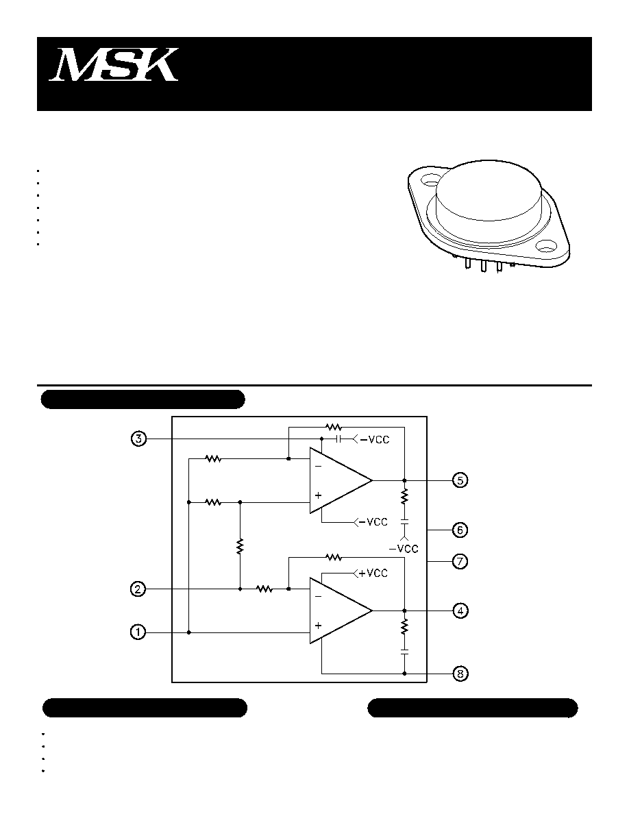
PIN-OUT INFORMATION
8
7
6
5
-VCC
N/C
N/C
OUTPUT 1
1
2
3
4
VREF
INPUT
+VCC
OUTPUT 2
EQUIVALENT SCHEMATIC
Rev. C 7/00
1
Group A
Subgroup
-
1
1
2,3
1
2,3
-
-
4
4
4
-
4
4
4
4
4
-
-
-
-
-
Total - Both Amplifiers V
IN
= 0V
V
IN
=0V
V
IN
=0V
V
CC
=±10V to ±15V
R
L
=1K
; F=10KHz
R
L
=10
; F=10KHz
F=10KHz
R
L
=10
; V
OUT
=10V
PP
V
OUT
=±10V
MSK121-1
MSK121-2
MSK121-5
MSK121-10
One Amplifier, DC Output
One Amplifier, AC Output F > 60Hz
Both Amplifiers, DC Output
Both Amplifiers, AC Output F > 60Hz
No Heat Sink
Test Storage Temperature Range
Lead Temperature Range
(Soldering 10 Seconds)
Case Operating Temperature
MSK121
MSK121B
Junction Temperature
ABSOLUTE MAXIMUM RATINGS
±V
CC
I
OUT
V
IND
V
INC
Total Supply Voltage
Peak Output Current
Differential Input Voltage
Common Mode Range
-65∞C to +150∞C
300∞C
-40∞C to +85∞C
-55∞C to +125∞C
+175∞C
T
ST
T
LD
T
C
T
J
MSK 121B
MSK 121
Parameter
Test Conditions
ELECTRICAL SPECIFICATIONS
1
Units
Min.
±2.5
-
-
-
-
-
-
60
±14
±13
±2.5
-
0.5
±0.9
±1.8
±4.8
±9.3
-
-
-
-
-
Typ.
±15
35
±1.5
±15
±30
±75
10
80
±14.2
±13.7
±3.5
40
1.5
±1.0
±2.0
±9.0
±10.0
5.0
3.7
3.4
2.4
30
Max.
±20
90
±10
±75
±1500
-
-
-
-
-
-
-
-
±1.1
±2.2
±5.4
±10.7
-
-
-
-
-
Min.
±2.5
-
-
-
-
-
-
60
±14
±13
±3
-
0.5
±0.95
±1.9
±4.75
±9.5
-
-
-
-
-
1
2
3
4
5
6
NOTES:
44
444
Max.
±20
60
±5
±50
±500
±1000
-
-
-
-
-
-
-
±1.05
±2.1
±5.25
±10.5
-
-
-
-
-
Typ.
±15
35
±0.5
±10
±30
±75
10
80
±14.2
±13.7
±4
40
1.5
±1.0
±2.0
±5.0
±10.0
5.0
3.7
3.4
2.4
30
30
30
30
30
30
40V
SOA
±VCC
±VCC-0.5V
V
mA
(mV)(Av)
µ
V/∞C
nA
nA
pF
dB
V
V
A
kHz
V/
µ
S
V/V
V/V
V/V
V/V
∞C/W
∞C/W
∞C/W
∞C/W
∞C/W
±VCC=±15 V, VREF=0V=GND, RL=1K
unless otherwise specified.
Parameter is guaranteed by design but not tested.
Typical specifications are representative of actual device performance at 25∞C but are for reference only.
Military grade devices ('B' suffix) shall be 100% tested to subgroups 1,2,3 and 4.
Subgroup 5 and 6 testing available upon request.
Subgroup 1,4 T
A
=T
C
=+25∞C
Subgroup 2,5 T
A
=T
C
=+125∞C
Subgroup 3,6 T
A
=T
C
=-55∞C
STATIC
Supply Voltge Range
2
Quiescent Current
INPUT
Output Offset Voltage
Output Offset Voltage Drift
2
Input Bias Current
2
Input Capacitance
2
Power Supply Rejection Ratio
2
OUTPUT
Output Voltage Swing
Output Peak Current
Power Bandwidth
3
TRANSFER CHARACTERISTICS
Slew Rate
2
Voltage Gain
THERMAL RESISTANCE
JC
(Junction to Case)
JC
JC
JC
JC
(Juction to Ambient)
Rev. C 7/00
2
APPLICATION NOTES
POWER SUPPLY CONNECTIONS
The MSK 121 maximum supply voltage is specified as ±20V.
However, single sided or unbalanced power supply operation
is permisible as long as the total power supply voltage does
not exceed 40V. Caution should be exercised when routing
high current printed circuit paths. Generally, these paths
should not be placed near low level, high impedance input
circuitry to avoid oscillations.
During initial evaluation, power supply current limiting is
strongly advised to avoid damaging the device. The MSK
121 has an internal 0.1
µ
F capacitor for high frequency
decoupling. However, both the negative and positive power
supplies must also be effectively decoupled with a low fre-
quency bypass capacitor to avoid power supply induced os-
cillation. An effective decoupling scheme consists of 10
µ
F
of capacitance for every 1 Amp of output current from each
power supply pin to ground. The capacitors will eliminate
any peak output voltage clipping which may occur due to
poor power supply load regulation. Power supply decoupling
capacitors should be placed as close to the package power
supply pins as possible (pins 3 and 8).
CURRENT LIMIT
The current limit circuitry is internal to the device. The typi-
cal value is shown in the parameter table. For protection
against high energy flyback conditions (inductive loads), fast
recovery reverse biased diodes should be connected from each
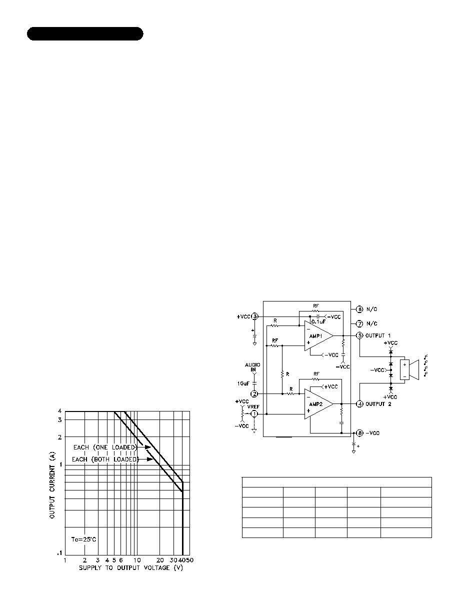
output to the power supplies. (See Figure 1.)
SAFE OPERATING AREA
The safe operating area curve is a graphical representation
of the power handling capability of the amplifier under vari-
ous conditions. The wire bond current carrying capability,
transistor junction temperature and secondary breakdown limi-
tations are all incorporated into the safe operation area curves.
All applications should be checked against the S.O.A. curves
to ensure high M.T.B.F.
VREF PIN CONNECTIONS
IN
The VREF pin is brought out to allow the user to bias the
outputs at a predetermined DC level. When the input signal
is AC coupled the output of each amplifier will be at the same
DC level as the VREF pin. This feature is very usefull when
using a single supply voltage. The user can simply connect a
resistor voltage divider to VREF to bias the output at one half
of the supply voltage by using 2 equal value resistors from
+VCC to -VCC (GND).
GAIN CONFIGURATIONS
The MSK 121 is available with preset gains of ±1, ±2, ±5
and ±10V/V. Refer to figure 1 for typical values of the inter-
nal components.
STABILITY CONSIDERATIONS
The MSK 121 has an internal RC snubber network on each
output for excellent stability for most applications. Good lay-
out practices should be used, however, when designing the
printed circuit board.
TYPICAL APPLICATION CIRCUIT
P/N
MSK121-1
MSK121-2
MSK121-5
MSK121-10
R
50K
25K
10K
10K
A
V
±1
±2
±5
±10
R
f
50K
50K
50K
100K
Figure 1
Z
IN
(V
REF
=GND)
33.3K
18.8K
8.6K
9.2K
Rev. C 7/00
3

