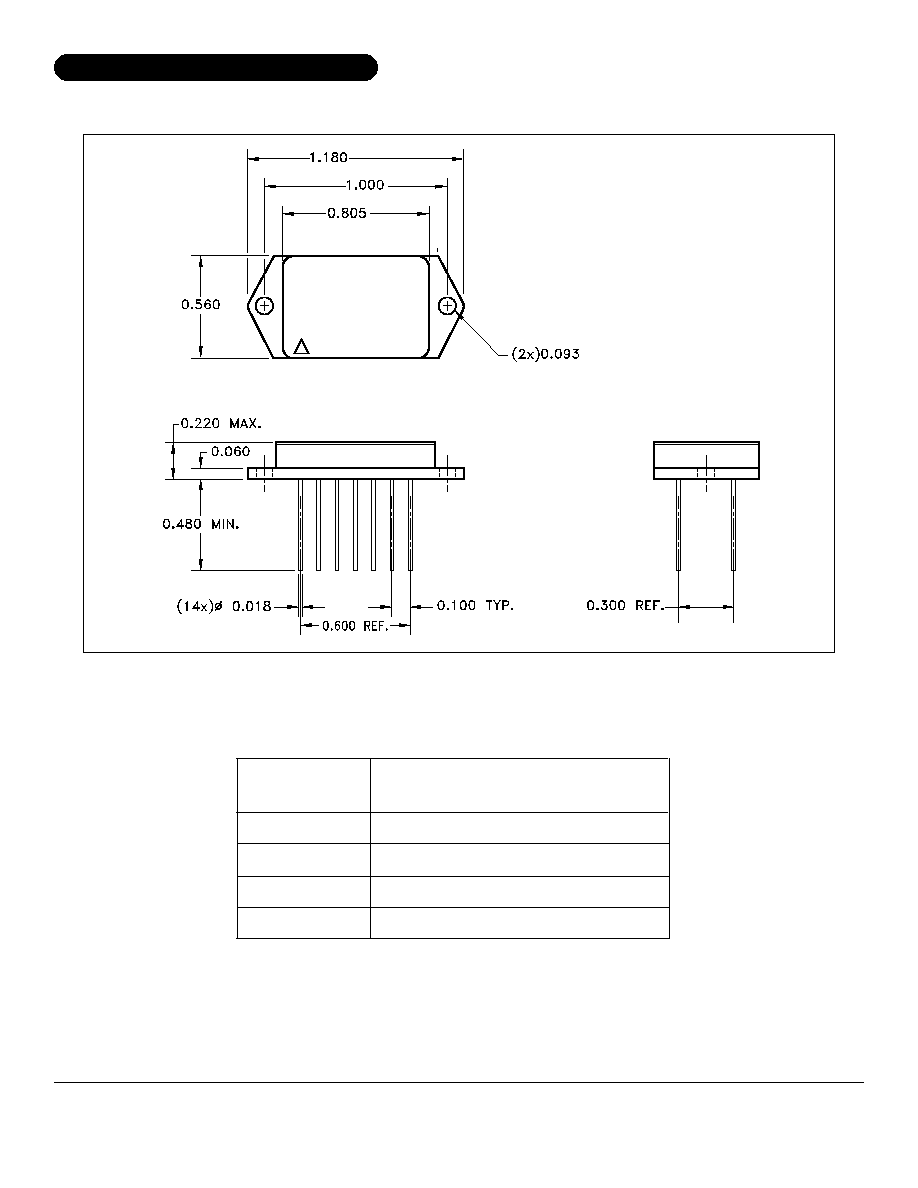
4707 Dey Road Liverpool, N.Y. 13088
(315) 701-6751
FEATURES:
Available to DSCC SMD #5962-02509HX
Space Efficient Dual Power Amplifier
Low Cost
High Voltage Operation: Up to 80V
Low Quiescent Current: 40mA Typ. Total
High Output Current: 5A Min. Per Amp
High Speed: 10V/µS Typ.
Monolithic Technology
Replaces obsolete MSK 154 up to 80V
MIL-PRF-38534 QUALIFIED
155
ISO-9001 CERTIFIED BY DSCC
M.S.KENNEDY CORP.
HIGH POWER DUAL
OPERATIONAL AMPLIFIER
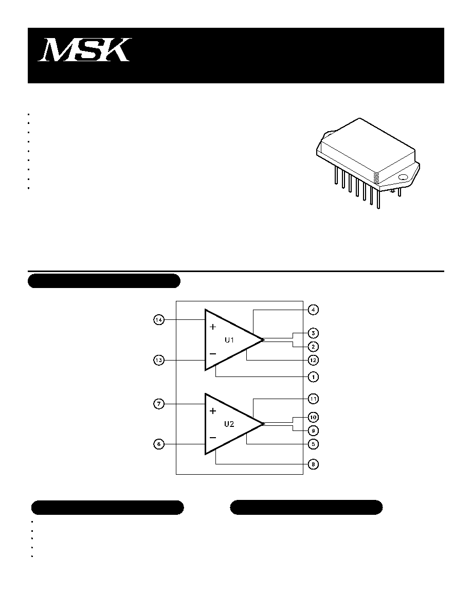
PIN-OUT INFORMATION
TYPICAL APPLICATIONS
PA Audio
Magnetic Deflection
Motor Drive
Noise Cancellation
High Power Bridge Amplifier
-Vcc1
Output Drive 1B
Output Drive 1A
+Vcc1
Current Sense 2
Inverting Input 2
Non Inverting Input 2
1
2
3
4
5
6
7
14
13
12
11
10
9
8
Non Inverting Input 1
Inverting Input 1
Current Sense1
+Vcc 2
Output Drive 2A
Output Drive 2B
-Vcc 2
EQUIVALENT SCHEMATIC
The MSK 155 is a high power dual monolithic operational amplifier ideally suited for high power amplification and
magnetic deflection applications. With a total supply voltage rating of 80 volts and 5A of available output current per
amplifier, the MSK 155 is also an excellent low cost choice for motor drive circuits. With both amplifiers in the same
package, thermally induced output offset voltages are eliminated. Power dissipation is kept to a minimum with a total
quiescent current rating of only 40mA. The MSK 155 is packaged in a hermetically sealed 14 pin power dip with heat
sink bolt down tabs.
DESCRIPTION:
Rev. A 12/01
1
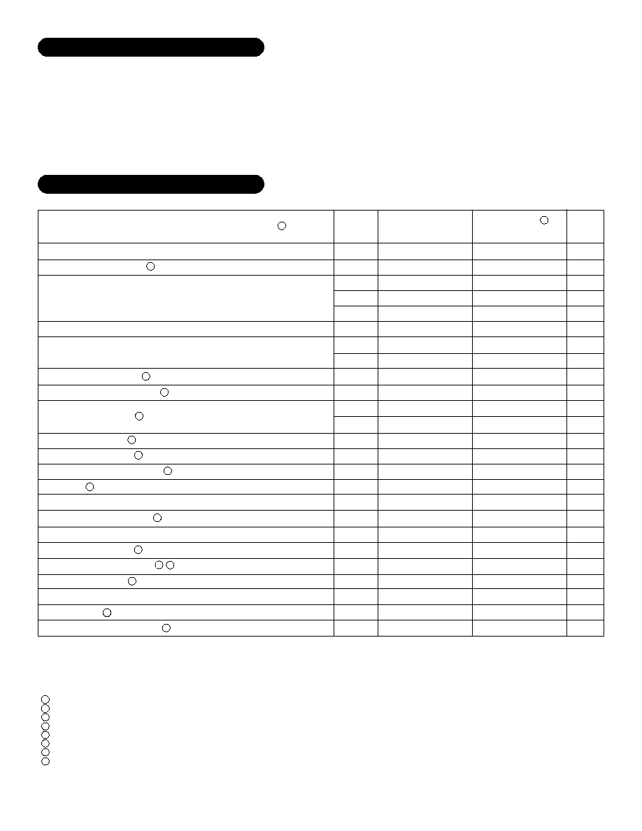
S T A T I C
Supply Voltage Range
I N P U T
Offset Voltage Drift
Offset Voltage vs ±Vcc
Input Impedance
Input Capacitance
Common Mode Rejection
Noise
OUTPUT
Output Voltage Swing
Output Voltage Swing
Power Bandwidth
Settling Time to 0.1%
Capacitive Load
TRANSFER CHARACTERISTICS
Slew Rate
Open Loop Voltage Gain
Max.
±40
±30
±30
±30
±2
±10
±50
-
±100
±10
-
-
-
-
-
-
-
-
-
-
-
80V
±5A
±Vcc
±Vcc
150∞C
Total Supply Voltage
Output Current (within S.O.A.)
Input Voltage (Differential)
Input Voltage (Common Mode)
Junction Temperature
-65∞C to +150∞C
300∞C
-55∞C to +125∞C
-40∞C to +85∞C
2.0∞C/W
1
2
3
4
5
6
7
8
ABSOLUTE MAXIMUM RATINGS
T
ST
T
LD
T
C
R
TH
V
CC
±I
OUT
V
IND
V
IN
T
J
Unless otherwise noted ±V
CC
= ±35VDC, RCL = 0
and specifications apply to each amplifier.
Typical parameters are for reference only.
A
V
=-1V/V measured in false summing junction circuit.
Devices shall be capable of meeting the parameter, but need not be tested.
Industrial grade and 'E' suffix devices shall be tested to subgroups 1 and 4 unless otherwise requested.
Military grade devices ('H' suffix) shall be 100% tested to subgroups 1,2,3 and 4.
Subgroup 5 and 6 testing available upon request.
Subgroup 1,4 T
C
=+25∞C
Subgroup 2,5 T
C
=+125∞C
Subgroup 3,6 T
A
=-55∞C
Storage Temperature
Lead Temperature
Case Operating Temperature
(MSK155H/E)
(MSK155)
Thermal Resistance (DC)
Junction to Case
V
IN
=0V
V
IN
=0V
(DC)
V
CM
=±22VDC
F = 10Hz to 1KHz
R
L
=10K
I
OUT
=5A Pk
R
L
= 10
V
OUT
=20VRMS
2V Step
A
V
=+10V/V
V
OUT
= ±10V R
L
= 10
F=10Hz R
L
= 10K
Group A
Subgroup
-
1
2
3
1
2,3
2,3
-
1
2, 3
-
-
4
-
-
4
4
-
-
4
4
Typ.
±35
±20
±20
±20
±0.1
±2
±10
±5
±20
-
10
5
110
10
±33.5
±30
55
2
-
10
100
Min.
±10
-
-
-
-
-
-
-
-
-
-
-
95
-
-
±29
45
-
10
6
95
Min.
±10
-
-
-
-
-
-
-
-
-
-
-
90
-
-
±29
40
-
10
6
90
Max.
±40
±35
-
-
±10
-
-
-
±200
-
-
-
-
-
-
-
-
-
-
-
-
Typ.
±35
±20
-
-
±0.1
-
±10
±5
±20
-
10
5
110
10
±33.5
±30
55
2
-
10
100
Units
V
mA
mA
mA
mV
mV
µV/∞C
µV/V
pA
nA
pF
dB
µV
RMS
V
V
KHz
µS
nF
V/µS
dB
MSK155H/E
MSK155
Parameter
4
Test Conditions
ELECTRICAL SPECIFICATIONS
2
2
1
4
2
NOTES:
4
4
12
12
Quiescent Current
3 2
4
4
4
2
5
Each Amp
V
IN
=0V
4
Rev. A 12/01
2
2
Offset Voltage
Input Bias Current
V
IN
=0V
V
CM
=0V
APPLICATION NOTES
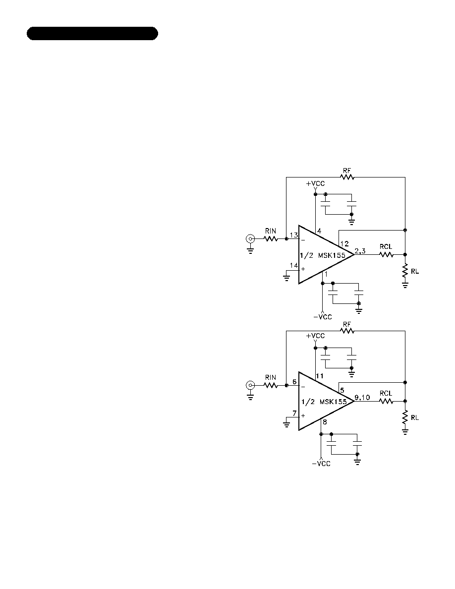
CURRENT LIMIT
(SEE TYPICAL CONNECTION DIAGRAM)
SAFE OPERATING AREA (SOA)
The output stage of this power operational amplifier has three
distinct limitations:
1. The current handling capability of the die metallization.
2. The junction temperature of the output device's.
3. Secondary breakdown.
All applications should be checked against the SOA curves.
NOTE: The output stage is protected against transient flyback.
However, for protection against sustained, high energy flyback,
external fast-recovery reverse biased diodes should be connected
from the output to ground.
R
CL
=(0.809V/I
CL
) - 0.057
A value of current limit resistance can be calculated as fol-
lows:
Where:
R
CL
is the current limit resistor value.
I
CL
is the current limit desired.
0.057
is the drop in the current limit path across internal
impedances other than the actual current limit resistor.
0.809
volts is the voltage drop that must be developed
across the current limit connections to activate the current
limit circuit at 25∞C.
It is recommended the user limit output current to a value as
close to the required output current as possible, without clip-
ping output voltage swing. Current limit will vary with case
temperature. Refer to the typical performance curves to pre-
dict current limit drift. If current limit is not required replace the
TYPICAL CONNECTION DIAGRAM
A 0.1 microfarad ceramic disc and low ESR capacitor with a
value of 10 microfarads per amp of output current should be
placed in parallel from each power supply pin to ground. These
capacitors must be rated for the full power supply voltage. Since
the MSK 155 is commonly used in circuits where the loop gain
is greater than 10 V/V, high frequency noise that enters the op-
amp through the power supply lines will be amplified and could
cause the amplifier to break into oscillation. In addition, with-
out supply bypassing, the inductance of the power supply lines
interacts with capacitive loads to form an oscillatory LC tank
circuit. The power supply decoupling capacitors will minimize
this effect and keep the circuit stable.
POWER SUPPLY DECOUPLING
Input protection circuitry within the MSK 155 will clip differ-
ential input voltages greater than V
CC
. The inputs are also
protected against common mode voltages up to the supply rails
as well as static discharge. There are current limiting resistors
in series with each input. These resistors may become dam-
aged in the event the input overload is capable of driving cur-
rents above 1mA. If severe overload conditions are expected,
external input current limiting resistors are recommended.
INPUT PROTECTION
It is recommended that the parallel sum of the input and feed-
back resistor be 1000 ohms or less to minimize phase shift
caused by the R-C network formed by the input resistor, feed-
back resistor and input capacitance. An effective method of
checking amplifier stability is to apply the worst case capaci-
tive load to the output of the amplifier and drive a small signal
square wave across it. If overshoot is less than 25%, the
system will typically be stable.
STABILITY
3
Rev. A 12/01