DESCRIPTION:
4707 Dey Road Liverpool, N.Y. 13088
(315) 701-6751
MIL-PRF-38534 QUALIFIED
166/167
ULTRA HIGH VOLTAGE
OPERATIONAL AMPLIFIER
ISO-9001 CERTIFIED BY DSCC
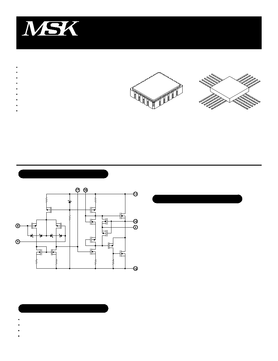
EQUIVALENT SCHEMATIC
Piezo Electric Positioning
Electrostatic Deflection
Computer to Vacuum Tube Interface
Ultra High Voltage Op-Amp Applications
TYPICAL APPLICATIONS
M.S.KENNEDY CORP.
MSK167
The MSK 166 and 167 ultra high voltage monolithic MOSFET operational amplifiers ideally suited for electrostatic
transducer and electrostatic deflection applications. With a total supply voltage rating of 350 volts and 60mA of
available output current, the MSK 166 and 167 are also an excellent low cost choice for high voltage piezo drive
circuits. The MOSFET output frees the MSK 166 and 167 from secondary breakdown limitations and power dissipa-
tion is kept to a minimum with a quiescent current rating of only 2mA. The MSK 166 is packaged in a hermetically
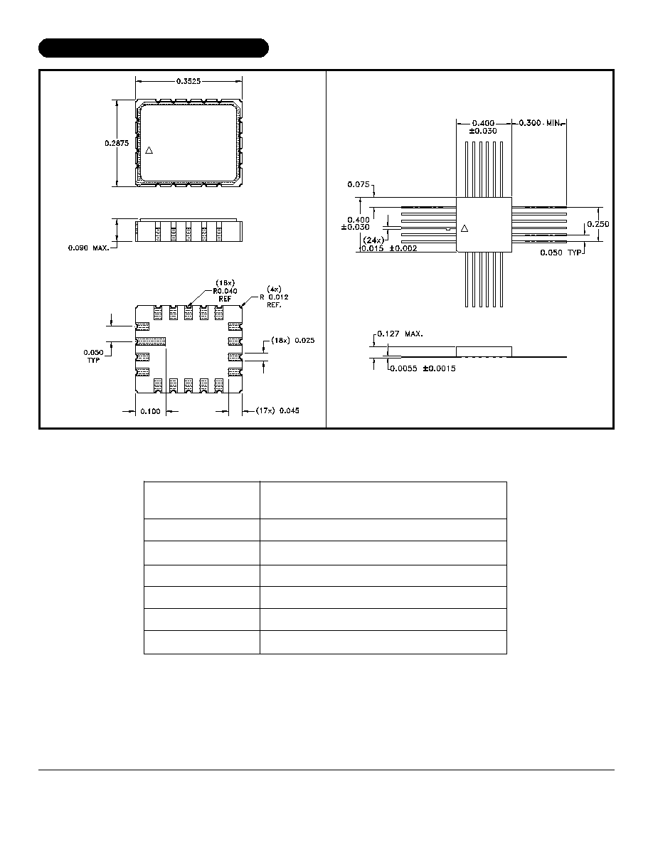
sealed 18 pin leadless chip carrier which has two external compensation pins. The MSK 167 is packaged in a 24 pin
ceramic flatpack and is otherwise identical to the MSK 166. (see mechanical specifications).
FEATURES:
Surface Mount Packages
Monolithic MOS Technology
High Voltage Operation - 350V
Low Quiescent Current - 2mA Max.
High Output Current - 60mA Min.
No Secondary Breakdown
High Speed - 40V/µS Typ.
External Compensation
Available to DSCC SMD 5962-96897
Rev. E 11/02
1
MSK166
The pin numbers shown in the above
schematic are for the MSK 166.
MSK 166 PINOUT
1
2
3
4
5
6
7
8
9
18
17
16
15
14
13
12
11
10
NC
Current Sense
NC
NC
NC
NC
NC
-Input
+Input
Comp2
Comp1
Output Drive
NC
+Vcc
NC
-Vcc
NC
NC
MSK 167 PINOUT
1
2
3
4
5
6
7
8
9
10
11
12
24
23
22
21
20
19
18
17
16
15
14
13
NC
NC
NC
NC
-Vcc
NC
+Vcc
Output Drive
NC
Compensation 1
Compensation 2
NC
NC
Non Inverting Input
Inverting Input
NC
NC
NC
NC
NC
NC
NC
Current Sense
NC
PIN-OUT INFORMATION

350V
60mA
120mA
±16V
±Vcc
150∞C
Total Supply Voltage
Output Current (within S.O.A.)
Output Current Peak
Input Voltage (Differential)
Input Voltage (Common Mode)
Junction Temperature
-65∞C to +150∞C
300∞C
-55∞C to +125∞C
-40∞C to +85∞C
15∞C/W
1
2
3
4
5
6
7
8
9
ABSOLUTE MAXIMUM RATINGS
T
ST
T
LD
T
C
R
TH
V
CC
±I
OUT
±I
OUTP
V
IND
V
IN
T
J
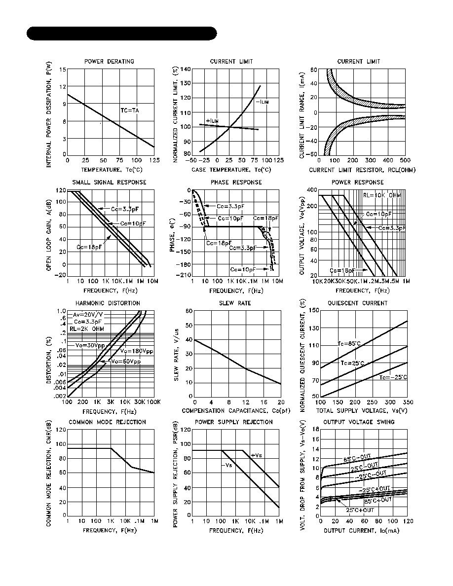
Unless otherwise noted C
C
=18pF, R
C
=2.2K
, ±V
CC
= ±150VDC.
Derate maximum supply voltage 0.5V/∞C below T
C
=+25∞C. No derating is needed above T
C
=25∞C.
A
V
=-10V/V measured in false summing junction circuit.
Devices shall be capable of meeting the parameter, but need not be tested. Typical parameters are for reference only.
Industrial grade and "E" suffix devices shall be tested to subgroups 1 and 4 unless otherwise specified.
Military grade devices ('B' suffix) shall be 100% tested to subgroups 1,2,3 and 4.
Subgroup 5 and 6 testing available upon request.
Subgroup 1,4 T
C
=+25∞C
Subgroup 2,5 T
C
=+125∞C
Subgroup 3,6 T
A
=-55∞C
Electrical specifications are derated for power supply voltages less than ±50VDC.
Storage Temperature
Lead Temperature
Case Operating Temperature
(MSK166B/E/167H/E)
(MSK166/167)
Thermal Resistance (DC)
Junction to Case
V
IN
=0V
V
IN
=0V
V
IN
=0V
V
IN
=0V
V
CM
=0V
(DC)
V
CM
=±90VDC
1Hz
f
10Hz
I
OUT
=±40mA Peak
V
OUT
=MAX
C
C
=10pF V
OUT
=280V
PP
No Load, R
CL
=0
C
C
=10pF 10V Step
A
V
=+1V/V
C
C
=Open
F=15Hz R
L
=5K
Group A
Subgroup
-
1
2
3
1
2,3
1
1,3
2
-
-
-
-
4
4
-
-
-
-
4
4
STATIC
Supply Voltage Range
INPUT
Offset Voltage
Offset Voltage Drift
Offset Voltage vs ±Vcc
Input Bias Current
Input Impedance
Input Capacitance
Common Mode Rejection
Noise
OUTPUT
Output Voltage Swing
Output Current
Power Bandwidth
Resistance
Settling Time to 0.1%
Capacitive Load
TRANSFER CHARACTERISTICS
Slew Rate
Open Loop Voltage Gain
Typ.
±150
±1.4
±2.0
±1.0
±15
±40
±20
±5
-
10
5
94
50
±141
±120
26
150
12
-
40
106
Min.
±50
-
-
-
-
-
-
-
-
-
-
84
-
±138
±60
-
-
-
10
20
94
Min.
±50
-
-
-
-
-
-
-
-
-
-
84
-
±138
±60
-
-
-
10
20
94
Max.
±175
±2.0
-
-
±30
-
±32
±100
-
-
-
-
-
-
-
-
-
-
-
-
-
Typ.
±150
±1.4
-
-
±15
±40
±20
±5
-
10
5
94
50
±141
±120
26
150
12
-
40
106
Units
V
mA
mA
mA
mV
µV/∞C
µV/V
pA
nA
pF
dB
µV
RMS
V
mA
KHz
µS
nF
V/µS
dB
MSK166B/E/167H/E
MSK166/167
2
Parameter
Max.
±175
±2.0
±3.0
±2.1
±30
±65
±32
±50
±50
-
-
-
-
-
-
-
-
-
-
-
-
4
Test Conditions
ELECTRICAL SPECIFICATIONS
4
4
1
4
4
3 4
NOTES:
4
4
4
2
9
4
4
11
11
4
Quiescent Current
Rev. E 11/02
2
APPLICATION NOTES
CURRENT LIMIT
Current limit resistor value can be calculated as follows:
It is recommended that the user set up the value of current limit
as close as possible to the maximum expected output current
to protect the amplifier. The minumum value of current limit
resistance is 33 ohms. The maximum practical value is 500
ohms. Current limit will vary with case temperature. Refer to
the typical performance graphs as a guide. Since load current
passes through the current limit resistor, a loss in output volt-
age swing will occur. The following formula approximates out-
put voltage swing reduction:
When the device is in current limit, there will be spurious oscil-
lations present on the negative half cycle. The frequency of
the oscillation is application dependant and can not be pre-
dicted. Oscillation will cease when the device comes out of
current limit. If current limit is not required simply short pin 2
and pin 16 (for the MSK 166).
R
CL
=3/I
LIM
V
R
=I
O
R
CL
*
INPUT PROTECTION
Input protection circuitry within the MSK 166/167 will clip
differential input voltages greater than 16 volts. The inputs are
also protected against common mode voltages up to the supply
rails as well as static discharge. There are 300 ohm current
limiting resistors in series with each input. These resistors may
become damaged in the event the input overload is capable of
driving currents above 1mA. If severe overload conditions are
expected, external input current limiting resistors are recom-
mended.
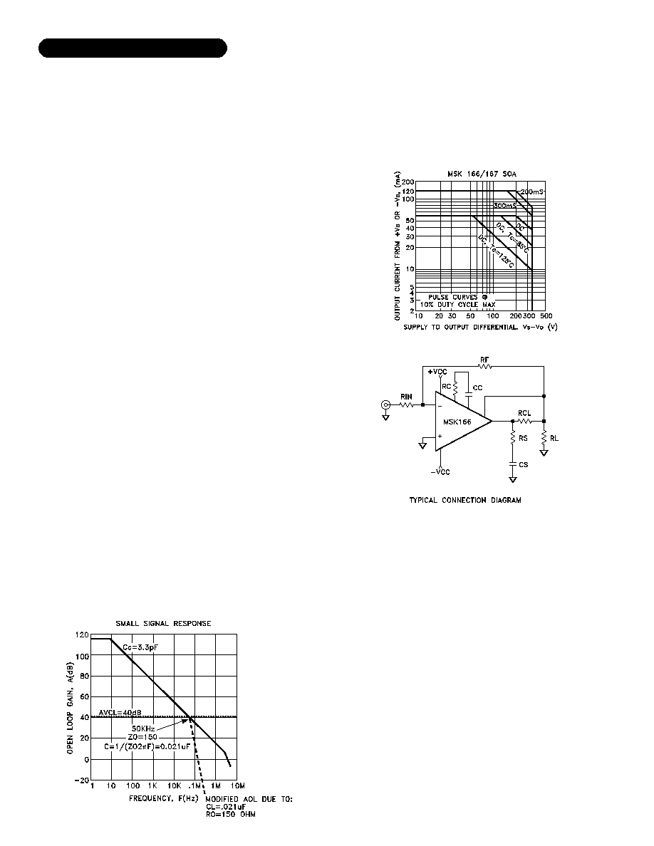
OUTPUT SNUBBER NETWORK
A 100 ohm resistor and a 330pF capacitor connected in se-
ries from the output of the amplifier to ground is recommended
for applications where load capacitance is less than 330pF.
For larger values of load capacitance, the output snubber net-
work may be omitted. If loop stability becomes a problem due
to excessively high load capacitance, a 100 ohm resistor may
be added between the output of the amplifier and the load. A
small tradeoff with bandwidth must be made in this configura-
tion. The graph below illustrates the effect of capacitive load
on open loop gain. Note that the compensation capacitor must
have a voltage rating greater than or equal to the total rail to rail
power supply voltage.
Rev. E 11/02
3
SAFE OPERATING AREA (SOA)
The MOSFET output stage of this ultra high voltage opera-
tional amplifier has two distinct limitations:
1. The current handling capability of the die metallization.
2. The junction temperature of the output MOSFET's.
NOTE: The output stage is protected against transient flyback.
However, for protection against sustained, high energy flyback,
external fast-recovery reverse biased diodes should be connected
from the output to ground.
STABILITY
The MSK 166/167 has sufficient phase margin when com-
pensated for unity gain to be stable with capacitive loads of at
least 10nF. However, it is recommended that the parallel sum
of the input and feedback resistor be 1000 ohms or less for
closed loop gains of ten or less to minimize phase shift caused
by the R-C network formed by the input resistor, feedback re-
sistor and input capacitance. The user can tailor the perfor-
mance of the MSK 166/167 to their application using the ex-
ternal compensation pins. The graphs of small signal gain and
phase as well as the graphs of slew rate and power response
demonstrate the effect of various forms of compensation. The
compensation capacitor must be rated at 350 volts working
voltage if maximum power supply voltages are used. The com-
pensation resistor and capacitor lead lengths must be kept as
short as possible to minimize spurious oscillations. A high quality
NPO capacitor rated for ±Vcc is recommended for the com-
pensation capacitor.
COMPENSATION
External compensation is only necessary at gains of 30v/v or
less. For larger gains, the compensation resistor and capacitor
may be omitted.