 | –≠–ª–µ–∫—Ç—Ä–æ–Ω–Ω—ã–π –∫–æ–º–ø–æ–Ω–µ–Ω—Ç: MSK182H | –°–∫–∞—á–∞—Ç—å:  PDF PDF  ZIP ZIP |
4707 Dey Road Liverpool, N.Y. 13088
(315) 701-6751
FEATURES:
Space Efficient Dual Amplifier
High Voltage Operation:
Single Supply: +8V to +60V
Dual Supply: ±4V to±30V
High Output Current: 3 Amp Continuous per amplifier
High Speed: 10V/µS
Low Quiescent Current: 20 mA per amplifier Typ.
Adjustable Current Limits
Thermal Shutdown
Monolithic Technology
Enable/Status Pin For Output Disable Control
MIL-PRF-38534 CERTIFIED
182/183
ISO-9001 CERTIFIED BY DSCC
Servo Driver
Actuator Driver
Audio Amplifier
Power Supplies
Bridge Amps
Stereo Amps
1
2
3
4
5
6
7
OUTPUT 1
+V
CC
1
-V
CC
1
+V
IN
2
-V
IN
2
I
LIM
2
E/S 2
14
13
12
11
10
9
8
E/S 1
I
LIM
1
-V
IN
1
+V
IN
1
-V
CC
2
+V
CC
2
OUTPUT 2
M.S.KENNEDY CORP.
MSK182
DESCRIPTION:
The MSK 182 and 183 are dual high power monolithic operational amplifiers ideal for use with a wide variety of loads. With
operation from either single or dual supplies, they offer excellent design flexibility. Power dissipation is kept to a minimum with a
quiescent current rating of only 20mA per amplifier, while 3 Amps of continuous available output current makes the MSK 182 or
MSK 183 a very good low cost choice for motor drive circuits and audio amplification. The design is internally protected against
current overloads and overtemperature conditions. Current limit can also be user-selected through the use of a resistor/potentiom-
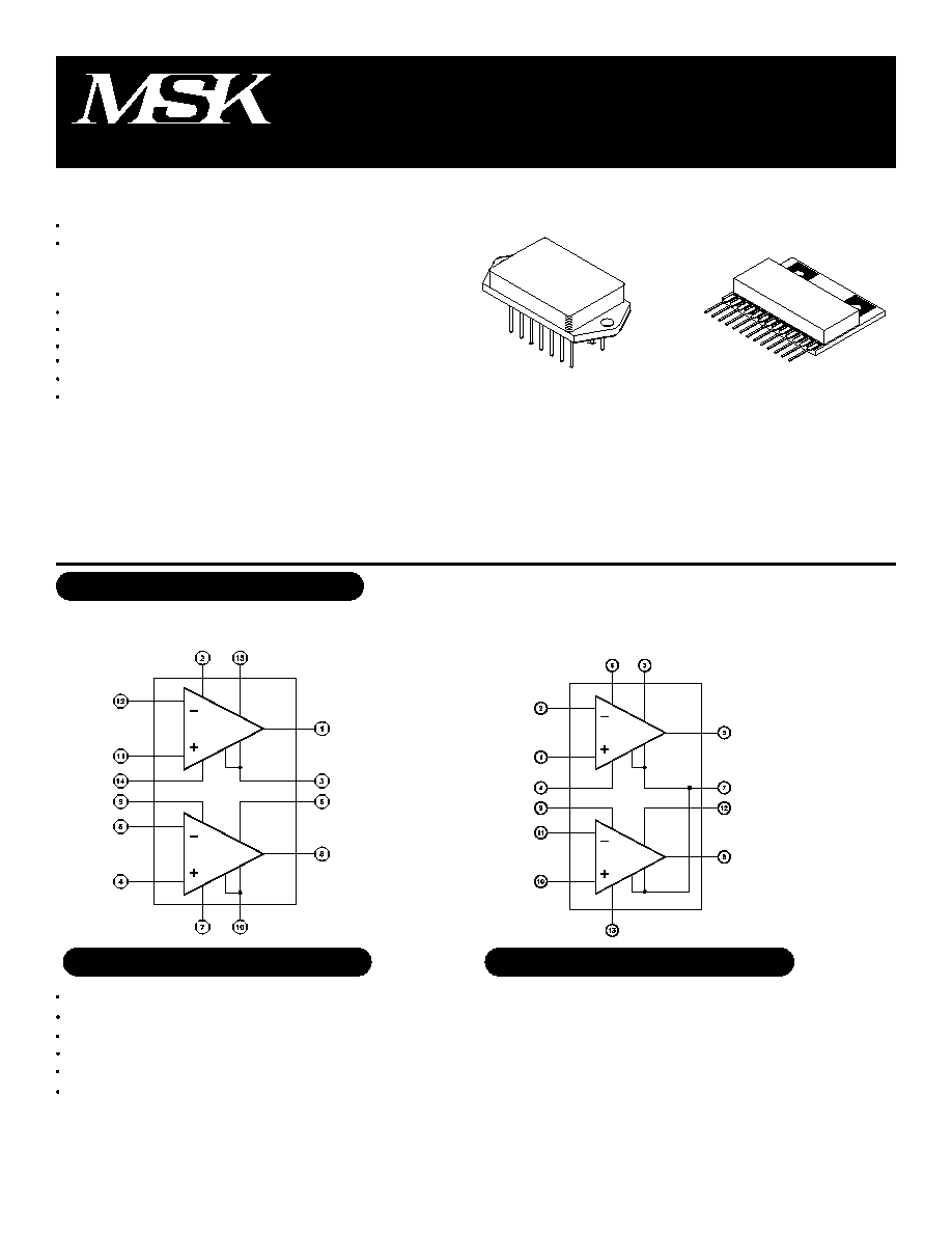
eter or voltage out/current out DAC. The MSK 182 is packaged in a hermetically sealed 14 pin power DIP with bolt down tabs for
applications that require heat sinking. The MSK 183 is packaged in a low cost ceramic SIP.
EQUIVALENT SCHEMATIC
PIN-OUT INFORMATION
TYPICAL APPLICATIONS
Rev. D 6/03
1
1
2
3
4
5
6
7
+V
IN
1
-V
IN
1
I
LIM
1
E/S
1
OUTPUT 1
+V
CC
1
-V
CC 1/2
MSK 182 PINOUT
MSK 183 PINOUT
13
12
11
10
9
8
E/S 2
I
LIM
2
-V
IN
2
+V
IN
2
+V
CC
2
OUTPUT 2
MSK183
DUAL HIGH VOLTAGE/
HIGH CURRENT
OPERATIONAL AMPLIFIER
MSK183
MSK182
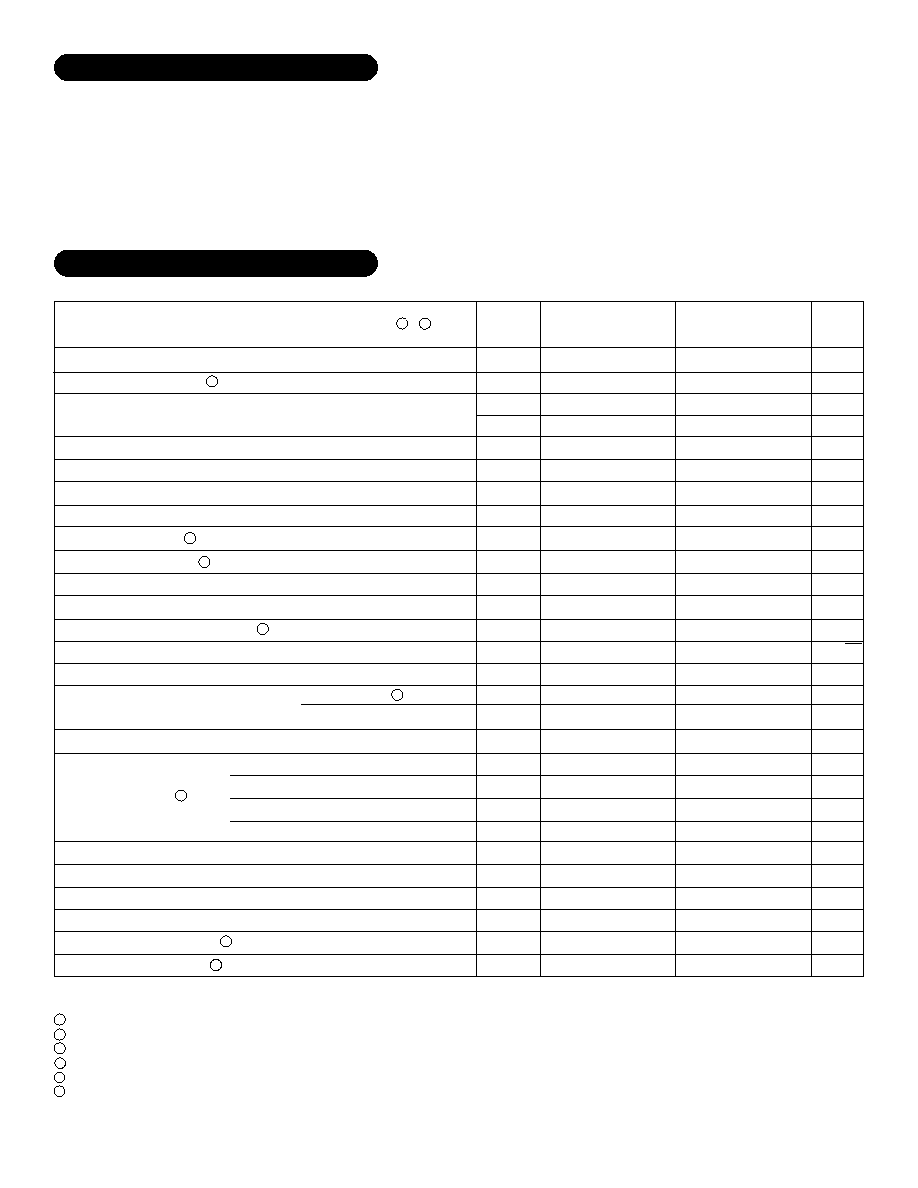
STATIC
Supply Voltage Range
INPUT
Input Offset Voltage
Input Offset Voltage Drift
Input Bias Current
Input Offset Current
Input Impedance
Input Capacitance
Common Mode Rejection Ratio
Input Voltage Noise Density
OUTPUT
Output Current
Output Disable Time
Output Enable Time
TRANSFER CHARACTERISTICS
Slew Rate
Open Loop Voltage Gain
Settling Time ±0.1%
Max.
±30
±20
±20
-
±10
-
±500
±50
-
-
-
-
-
-
-
-
-29
-
-
-
-
-
-
-
60V
5A
±29.5V
+27V/-29V
Internal Protection
(See Application Note)
Total Supply Voltage
Output Current (within S.O.A.)
Input Voltage (Differential)
Input Voltage (Common Mode)
Junction Temperature
-65∞C to +150∞C
300∞C
-55∞C to +125∞C
-40∞C to +85∞C
1.8∞C/W
3.0∞C/W
1
2
3
4
5
6
ABSOLUTE MAXIMUM RATINGS
T
ST
T
LD
T
C
R
TH
V
CC
±I
OUT
V
IND
V
IN
T
J
Unless otherwise specified ±V
CC
= ±30VDC and E/S pin is open.
All electrical specifications apply to each amplifier.
Devices shall be capable of meeting the parameter, but need not to be tested. Typical parameters are for reference only.
Industrial grade and 'E' suffix devices shall be tested to subgroups 1 and 4 unless otherwise specified.
Military grade devices ('H' suffix) shall be 100% tested to subgroups 1,2,3 and 4.
Subgroup 1,4 T
A
=T
C
=+25∞C
Subgroup 2
T
A
=T
C
=+125∞C
Subgroup 3
T
A
=T
C
=-55∞C
Storage Temperature Range
Lead Temperature Range
(10 seconds)
Case Operating Temperature
(MSK182H/E)
(MSK182/183)
Thermal Resistance
Junction to Case (Per Amplifier)MSK182
Junction to Case (Per Amplifier)MSK183
V
IN
=0V
V
IN
=0V
V
IN
=0V
V
IN
=OV
f=DC
f=DC
(-V
CC
)-
0.1
V
IN
(+V
CC)
-
3V
f=1KH
Z
I
OUT
=0.6A
I
OUT
=3.0A
DC=Continuous
V
E/S
High- Output Enabled E/S Open or High
V
E/S
Low- Output Disabled E/S Forced Low
I
E/S
High- Output Enabled E/S Open or High
I
E/S
Low- Output Disabled E/S Forced Low
A
V
=1 V
OUT=
50Vp-p R
L
=8
V
OUT
=±25V R
L
=1K
A
V
=10 50V Step
Group A
Subgroup
-
1
2,3
-
1
-
1
1
-
-
1
-
4
4
4
4
4
-
-
-
-
-
4
-
Typ.
-
±17
±17
±6
±2
±30
±100
±5
10
6
95
90
±28
±26
-
-
-
-65
-70
1
3
10
98
15
Min.
±4
-
-
-
-
-
-
±1
-
-
80
-
±27
±25.5
±3
-27.5
-
-
-
-
-
-
90
-
Min.
±4
-
-
-
-
-
-
-
-
-
75
-
±27
±25
±3
-27.5
-
-
-
-
-
-
88
-
Max.
±30
±23
-
-
±15
-
±750
±75
-
-
-
-
-
-
-
-
-29
-
-
-
-
-
-
-
Typ.
-
±17
-
±6
±2
±30
±100
±5
10
6
95
90
±28
±26
-
-
-
-65
-70
1
3
8
98
18
Units
V
mA
mA
mA
mV
µV/∞C
n
A
n
A
pF
dB
nV/
H
Z
V
V
A
V
V
µA
µA
µS
µS
V/µS
dB
µS
MSK182H/E
MSK182/MSK 183
Parameter
Test Conditions
ELECTRICAL SPECIFICATIONS
1
NOTES:
Quiescent Current (Per Amp)
2
Quiescent Current (Per Amp)
V
IN
=0V
Shutdown Mode V
IN
=0V
7
7
Shutdown Input
Output Voltage Swing
3
3
3
3
3
2
3
3
Rev. D 6/03
3

APPLICATION NOTES
POWER SUPPLIES:
For the MSK 182/183 maximum total supply voltage is speci-
fied as 60V. However, dual and unbalanced power supply op-
eration is permissible as long as total supply voltage does not
exceed 60V.
POWER SUPPLY BYPASSING:
Power supply terminals must be effectively decoupled with a
high and low frequency bypass circuit to avoid power supply
induced oscillation. An effective decoupling scheme consists
of a 0.1µF ceramic capacitor in parallel with a 10µF tantalum
capacitor for each power supply pin to ground. In addition, it is
recommended that a 0.01µF capacitor be placed between ±Vcc
as close to the MSK 182 as possible.
COMPENSATION:
For normal operation output compensation is not typically
required. However, if the MSK 182 or MSK 183 is intended to
be driven into current limit the user may find that an R/C net-
work is required. A snubber network from the output to ground
for each amplifier will provide stability. If driving large capaci-
tive or inductive loads, a snubber network will also enhance
stability. Typically 3
to 10
in series with 0.01µF is accept-
able.
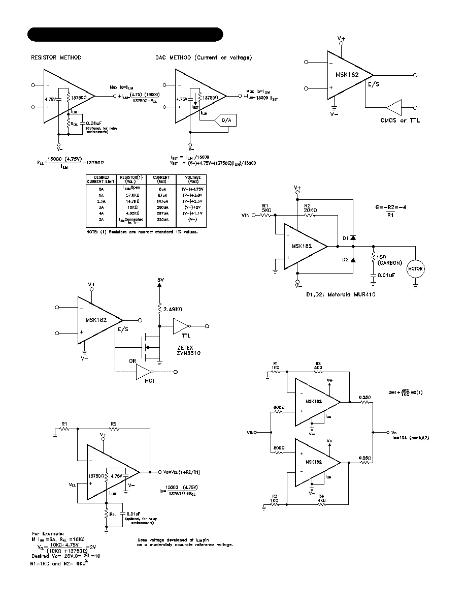
CURRENT LIMIT:
The MSK 182 and MSK 183 offer accurate, user-selectable
current limit. Unlike typical designs that use a power resistor in
series with the output to sense load, the MSK 182 and MSK
183 sense the load indirectly and therefore do not require a
resistor to handle the full output current. Current limit is se-
lected by controlling the input to the I
LIM
pin.
The easiest method is to use a resistor or potentiometer con-
nected between-Vcc and the I
LIM
pin. Use the following equa-
tion to select proper resistor value:
71,250
I
LIM
A low level control signal (0-330µA) can also be used to con-
trol the current level digitally. If the pin is left open, the current
is programmed to OA, while connecting I
LIM
directly to -Vcc
sets the output current to it's maximum, typically 5A.
The MSK 182 and MSK 183 are equipped with thermal pro-
tection circuitry that protects each amplifier from damage caused
by excessive junction temperature. The output is disabled when
the junction temperature reaches approximately 160∞C. After
the junction temperature cools to approximately 140∞C, the
output is again enabled. The thermal protection may cycle on
and off depending on the output load and signal conditions;
this may have an undesirable effect on the load.
It should be noted that even though this internal protection
circuitry does protect against overload conditions, it does not
take the place of proper heat sinking. For reliable operation,
junction temperature should be limited to 150∞C, maximum.
TYPICAL CONNECTION DIAGRAM
Rev. D 6/03
3
SAFE OPERATING AREA:
The safe operating area curve is a graphical representation of
the power handling capability of the amplifier under various
conditions. Power dissipation of the device is equal to the prod-
uct of the voltage across the output transistor times the output
current. As can be seen in the curve, safe operating current
decreases with an increase in temperature as well as an in-
crease in the voltage across the output transistor. Therefore,
for maximum amplifier performance it is important to keep case
temperature as low as possible and to keep ±Vcc as close to
the output rail as achievable.
THERMAL PROTECTION:
This pin actually has a dual function. First, when the pin is
forced low, the output stage is disabled. Second, it can be
monitored to determine if the device is in thermal shutdown.
These functions can be used on the same device with either
single or dual supplies. For normal operation, the E/S pin must
be left open or pulled at least 2.4 volts above the negative rail.
In noisy applications, a small value capacitor between the E/S
pin and -Vcc may be required.
ENABLE/STATUS PIN:
To disable the output, the user must pull the E/S pin low, no
greater than 0.8V above -Vcc. To once again enable the de-
vice, the E/S pin must be brought at least 2.4 volts above -Vcc
or be disconnected. It should be noted that when the E/S pin is
high, the internal thermal shutdown is still active.
If the E/S pin is used to monitor thermal shutdown, during
normal operation the voltage on the E/S pin is typically 3.5V
above -Vcc. Once shutdown has occurred this voltage will drop
to approximately 350mV above -Vcc.
-13.75K
Rcc=
4
Rev. D 6/03
APPLICATION NOTES cont.
Figure 1
Figure 3
Figure 5
Figure 6
Figure 4
Figure 2
Output Disable with a Single Supply
Adjustable Current Limit
Thermal Shutdown Status With a Single Supply
Voltage Source
Parallel Output For Increased Output Current
Motor Drive Circuit

TYPICAL PERFORMANCE CURVES
5
Rev. D 6/03
GENERAL PART NUMBER
NOTE: THE MSK 183 IS NOT AVAILABLE WITH E OR H SUFFIX.
ORDERING INFORMATION
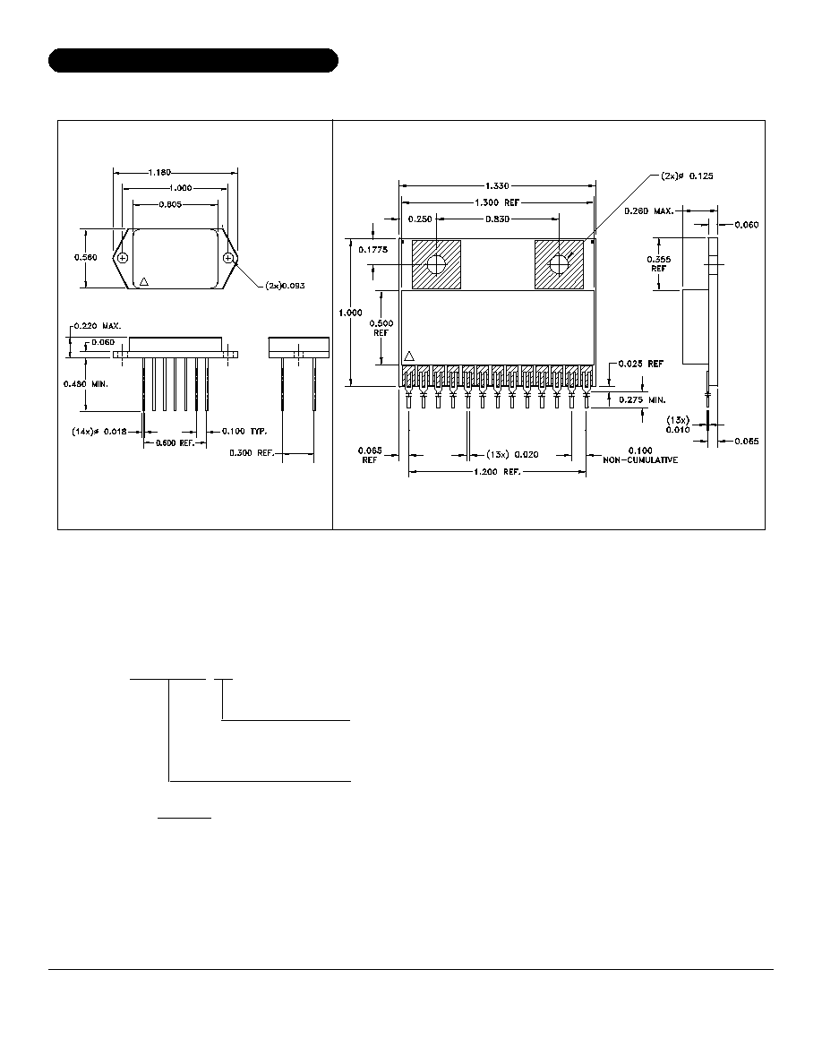
MECHANICAL SPECIFICATIONS
ESD TRIANGLE INDICATES PIN 1.
The information contained herein is believed to be accurate at the time of printing. MSK reserves the right to make
changes to its products or specifications without notice, however, and assumes no liability for the use of its products.
Please visit our website for the most recent revision of this datasheet.
M.S. Kennedy Corp.
4707 Dey Road, Liverpool, New York 13088
Phone (315) 701-6751
FAX (315) 701-6752
www.mskennedy.com
MSK 182
MSK182
MSK183
Rev. D 6/03
6
H
SCREENING
BLANK = INDUSTRIAL; E = EXTENDED RELIABILITY
H = MIL-PRF-38534
ALL DIMENSIONS ARE ±0.010 INCHES UNLESS OTHERWISE LABELED.