4707 Dey Road Liverpool, N.Y. 13088
M.S.KENNEDY CORP.
(315) 701-6751
3554
FEATURES:
Stable at Low Gain
Fast Slew Rate - 1200V/µs Typical
Gain Bandwidth Product - 1200 MHz Typical
Low Quiescent Current - ±14.0 mA Typical
Low Offset - 2 mV Maximum
Drop In Replacement for OPA 3554 and TP 3554
High Output Current - ±100mA Minimum
DESCRIPTION:
The MSK 3554 is a pin compatible, low gain stable, drop-in replacement for the OPA 3554 and TP 3554. The
MSK 3554 does not exhibit high frequency output oscillations like other versions of the 3554 when operated at
closed loop gains of less than 55 V/V. The extremely low input bias current and input offset voltage ratings coupled
with a high slew rate and wide bandwidth make the MSK 3554 an excellent choice for fast D/A converters, buffers,
pulse amplifiers and other high speed op-amp applications. The MSK 3554 is packaged in an 8-pin TO-3 using thick
film hybrid technology to obtain high reliability and compact size.
Fast D/A Converters
Pulse Amplifiers
Video Instrumentation
Fast Buffer/Follower
Video Frequency Filters
Balance
Negative Power Supply
Non-Inverting Input
Inverting Input
1
2
3
4
Output
Positive Power Supply
Compensation
Balance
8
7
6
5
TYPICAL APPLICATIONS
PIN-OUT INFORMATION
HIGH SPEED, WIDEBAND
OPERATIONAL AMPLIFIER
EQUIVALENT SCHEMATIC
MIL-PRF-38534 QUALIFIED
ISO 9001 CERTIFIED BY DSCC
Rev. B 7/00
1
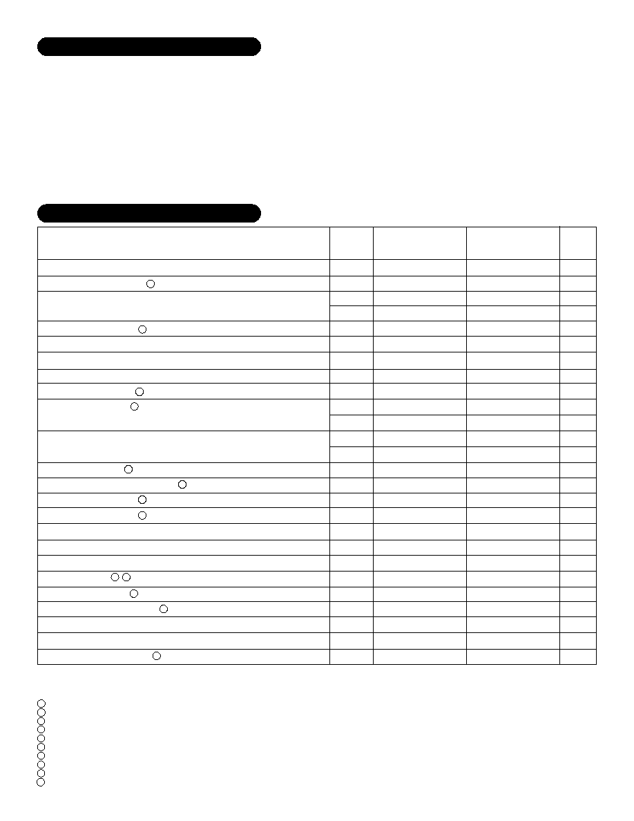
STATIC
Supply Voltage Range
Quiescent Current
Thermal Resistance
INPUT
Input Offset Voltage
Input Offset Voltage Drift
Input Offset Adjust
Input Bias Current
Input Offset Current
Input Impedance
Power Supply Rejection Ratio
Input Noise Density
Input Noise Voltage
OUTPUT
Output Voltage Swing
Output Current
Settling Time
Power Bandwidth
Bandwidth (Small Signal)
TRANSFER CHARACTERISTICS
Slew Rate
Open Loop Voltage Gain
ABSOLUTE MAXIMUM RATINGS
T
ST
T
LD
P
D
T
J
Storage Temperature Range
Lead Temperature Range
(10 Seconds)
Power Dissipation
Junction Temperature
Supply Voltage
Peak Output Current
Differential Input Voltage
Case Operating Temperature
MSK 3554B
MSK 3554
-65∞C to +150∞C
300∞C
See Curve
175∞C
Unless otherwise specified ±V
CC
=±15V
DC
AV=-1, measured in false summing junction circuit.
Devices shall be capable of meeting the parameter, but need not be tested. Typical parameters are for reference only.
Industrial grade devices shall be tested to subgroups 1 and 4 unless otherwise specified.
Military grade devices ('B' suffix) shall be 100% tested to subgroups 1,2,3 and 4.
Subgroup 5 and 6 testing available upon request.
Subgroup 1,4 T
A
=T
C
=+25∞C
Subgroup 2,5 T
A
=T
C
=+125∞C
Subgroup 3,6 T
A
=T
C
=-55∞C
Measurement taken .5 second after application of power using automatic test equipment.
NOTES:
±18V
±150mA
±25V
-55∞C to +125∞C
-40∞C to +85∞C
±V
CC
I
OUT
V
IN
T
C
1
2
3
4
5
6
7
8
9
Min.
±12
-
-
-
-
-
-
-
-
-
-
80
-
-
±10.5
±100
-
16
70
800
90
Max.
±18
±20
±30
-
±2.0
±50
±50
±50
±25
±30
-
-
-
-
-
-
150
-
-
-
-
Min.
±12
-
-
-
-
-
-
-
-
-
-
80
-
-
±10
±100
-
15
70
750
88
Max.
±18
±20
-
-
±3.0
-
±100
-
±30
-
-
-
-
-
-
-
150
-
-
-
-
Units
V
mA
mA
∞C/W
mV
µV/∞C
mV
pA
nA
pA
nA
dB
nV
Hz
µVrms
V
mA
nS
MHz
MHz
V/µS
dB
MSK 3554B
11
11
MSK 3554
Adjust to Zero
Adjust to Zero
ELECTRICAL SPECIFICATIONS
10
3
3
3
3
3
2
Typ.
±15
±14
-
37
±0.5
±20
±10
±10
±2.0
±2.0
10
110
15
10.0
±12
±120
120
19
90
1200
96
Typ.
±15
±14
-
37
±0.5
±20
±20
-
±2.0
-
10
110
15
10.0
±12
±120
120
19
90
1200
96
Test Conditions
Group A
Subgroup
-
1
2,3
-
1
2,3
1,2,3
1
2,3
1
2,3
-
-
-
-
4
4
4
4
4
4
4
V
IN
=0V
A
V
=-1
V/V
Junction to Case Output Devices
Bal.Pins=N/C V
IN
=0V A
V
=-10
V/V
V
IN
=0V
R
POT
=20K
To +V
CC
A
V
=-1
V/V
V
CM
=0V Either Input
V
CM
=0V
F=DC Differential
V
CC
=10V
F=1KHz
F=10Hz To 1MHz
R
L
=100
T
J
<150∞C
0.1% 10V step
R
L
=100
V
O
=±10V C
C
=0
C
C
=0
V
OUT
=±10V R
L
=100
C
C
=0
C
C
=0 R
L
=100
F=1KHz V
OUT
=±10V
Parameter
3
3
3
3
3
3
10
2
Rev. B 7/00

APPLICATION NOTES
HEAT SINKING
Refer to the following thermal model and governing equa-
tions to determine appropriate heat sinking for your application.
Example:
This example demonstrates a worst case analysis for the op-
amp output stage. This occurs when the output voltage is 1/2
the power supply voltage. Under this condition, maximum power
transfer occurs and the output is under maximum stress.
Conditions:
V
CC
= ±16VDC
V
O
= ±8Vp Sine Wave, Freq. = 1KHZ
R
L
= 100
Governing Equation:
T
J
=P
D
x (R
JC
+ R
CS
+ R
SA
) + T
A
Where
T
J
= Junction Temperature
P
D
= Total Power Dissipation
R
JC
= Junction to Case Thermal Resistance
R
CS
= Case to Heat Sink Thermal Resistance
R
SA
= Heat Sink to Ambient Thermal Resistance
T
C
= Case Temperature
T
A
= Ambient Temperature
T
S
= Sink Temperature
For a worst case analysis we will treat the +8Vp sine wave
as an 8 VDC output voltage.
1.) Find Driver Power Dissipation
P
D
= (V
CC
-V
O
) (V
O
/R
L
)
= (16V-8V) (8V/100
)
= .64W
2.) For conservative design, set T
J
=+125∞C
3.) For this example, worst case T
A
=+90∞C
4.) R
JC
= 37∞C/W from MSK 3554B Data Sheet
5.) R
CS
= 0.15∞C/W for most thermal greases
6.) Rearrange governing equation to solve for R
SA
R
SA
= ((T
J
- T
A
)/P
D
) - (R
JC
) - (R
CS
)
= ((125∞C - 90∞C) / .64W) - 37∞C/W - .15∞C/W
= 54.7 - 37.15
= 17.54∞C/W
The heat sink in this example must have a thermal resistance
of no more than 17.54∞C/W to maintain a junction temperature
of no more than +125∞C.
OFFSET NULL
Typically, the MSK 3554(B) has an input offset voltage of
less than ±0.5mV. If it is desirable to adjust the offset closer
to "zero", or to a value other than "zero", the circuit below is
recommended. Rp should be a ten-turn 20K
potentiometer.
Typical offset adjust is ±20mV.
Thermal Model:
GAIN
-1
-10
-100
follower
Rfb
5.6K
5.6K
10K
0
Cfb
2.0pF
1.2pF
0.0pF
0pF
Ccomp
10pF
10pF
0.0pF
12pF
Rin
5.6K
560
100
0
COMPONENT SELECTION TABLE
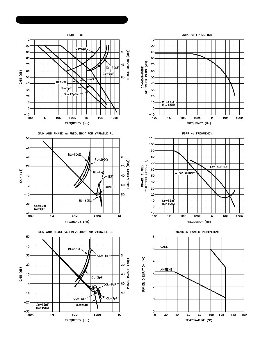
COMPENSATION
The compensation capacitor is connected between pins 1
and 3 and is used to optimize bandwidth and slew rate while
maintaining circuit stability. The effect of compensation ca-
pacitance can be seen in the Bode Plot under the Typical Perfor-
mance Curves. As closed loop gain increases, compensation
capacitance can decrease and higher slew rates and wider band-
widths will be realized. See the component selection table for
recommended values of input and feedback resistance as well
as feedback capacitance and compensation capacitance.
3
Rev. B 7/00

TOP VIEW PIN REFERENCES SHOWN.
ORDERING INFORMATION
Screening Level
MSK3554
Industrial
The information contained herein is believed to be accurate at the time of printing. MSK reserves the right to make
changes to its products or specifications without notice, however, and assumes no liability for the use of its products.
MECHANICAL SPECIFICATIONS
M.S. Kennedy Corp.
4707 Dey Road, Liverpool, New York 13088
Phone (315) 701-6751
FAX (315) 701-6752
www.mskennedy.com
MSK3554B
Military-Mil-PRF-38534
Rev. B 7/00
Part
Number
5
ALL DIMENSIONS ARE ±0.010 INCHES UNLESS OTHERWISE LABELED