 | –≠–ª–µ–∫—Ç—Ä–æ–Ω–Ω—ã–π –∫–æ–º–ø–æ–Ω–µ–Ω—Ç: MSK4203S | –°–∫–∞—á–∞—Ç—å:  PDF PDF  ZIP ZIP |
4707 Dey Road Liverpool, N.Y. 13088
(315) 701-6751
M.S.KENNEDY CORP.
ISO 9001 CERTIFIED BY DSCC
4203
75 VOLT 10 AMP
H-BRIDGE PWM MOTOR
DRIVER/AMPLIFIER
MIL-PRF-38534 QUALIFIED
FEATURES:
75 Volt, 10 Amp Capability
Self-Contained Smart Lowside/Highside Drive Circuitry
Internal PWM Generation, Shoot-through Protection
Isolated Case Allows Direct Heatsinking
On Board 5 Volt Regulator
Available Fully Screened To MIL-PRF-38534 Class H
Logic Level High Side Enable Control
Logic Level Disable Input
TYPICAL APPLICATIONS
Rev. A 10/02
1
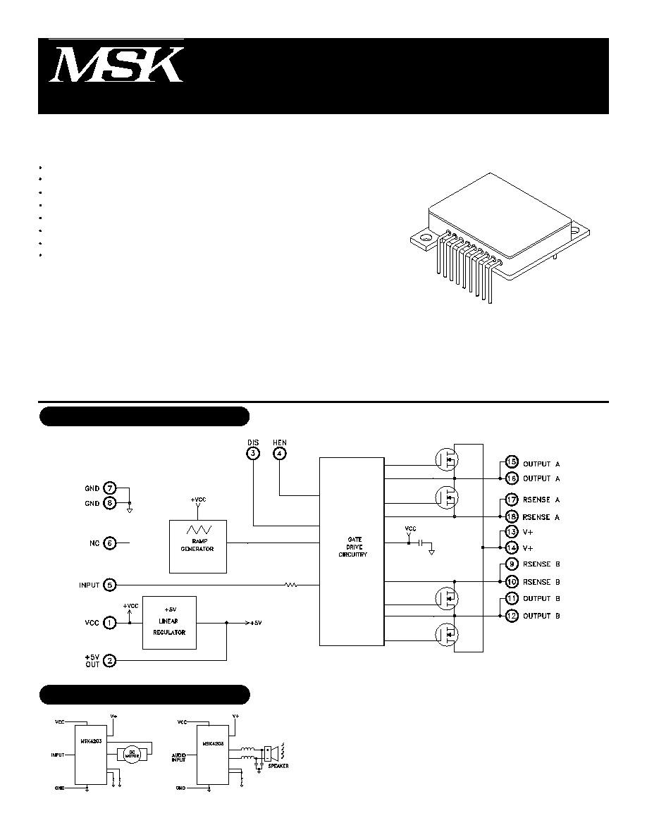
DESCRIPTION:
The MSK 4203 is a complete H-Bridge hybrid intended for use in DC brushed motor control applications or Class D
switchmode amplification. All of the drive/control circuitry for the lowside and highside switches are internal to the hybrid,
as well as a +5V linear regulator. The PWM circuitry is internal as well, leaving the user to only provide an analog signal
for the motor speed/direction, or audio signal for switchmode audio amplification. The MSK 4203 is packaged in a space
efficient isolated 18 pin power package available in three lead form configurations that can be directly connected to a
heatsink.
EQUIVALENT SCHEMATIC
Rev. A 10/02
1
2
3
4
5
6
NOTES:
V
CC
=
12V
,
V+=28V
,
R
SENSE
A,B=Ground, DIS=OV, HEN=NC unless otherwise specified.
Guaranteed by design but not tested. Typical parameters are representative of actual device performance but are for reference only.
Devices shall be 100% tested to subgroups 1,2,3 and 4. Subgroup 5 and 6 testing available upon request.
Subgroup 1,4,7
T
A
=T
C
=
+25∞C
2,5
T
A
=T
C
=
+125∞C
3,6
T
A
=
T
C
=
-55∞C
Industrial grade and "E" suffix devices shall be 100% tested at 25∞C only.
The internal on resistance is for the die only. This should be used for thermal calculations only.
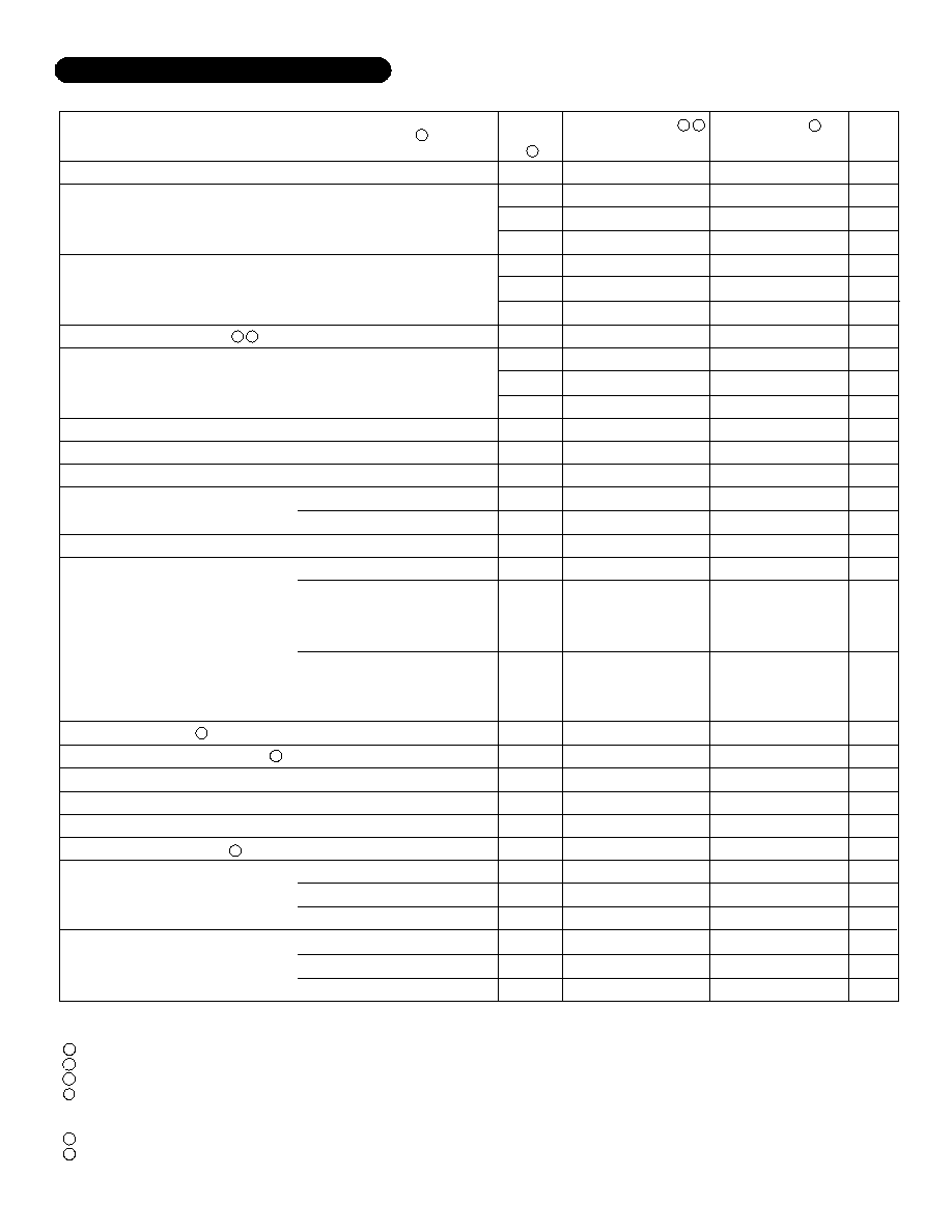
ELECTRICAL SPECIFICATIONS
22
2
OUTPUT CHARACTERISTICS
VDS (ON) Voltage (Each Mosfet)
Instantaneous Forward Voltage
(Each Intrinsic Diode)
RDS (ON) (Each Mosfet)
Leakage Current, Each Mosfet
PWM Frequency
V
CC
SUPPLY CHARACTERISTICS
Quiescent Current
+5V Output
OUTPUT DUTY CYCLE
Analog Input Current
SWITCHING CHARACTERISTICS
Rise Time
Fall Time
Dead Time
LOGIC CONTROL INPUTS
DIS Input
HEN Input
Group A
1
2
3
1
2
3
-
1
2
3
4,5,6
1,2,3
1,2,3
1,2,3
4,5,6
7
7
-
4
4
4
1,2,3
1,2,3
1,2,3
1,2,3
1,2,3
1,2,3
Min.
-
-
-
-
-
-
-
-
-
-
40
-
4.85
4.8
40
-
-
-
-
-
-
-
2.7
-
-
2.7
-
Max.
1.2
-
-
2.0
-
-
0.13
100
-
-
50
50
5.15
5.2
60
-
-
5
TBD
TBD
TBD
0.8
-
150
0.8
-
300
Typ.
0.5
-
-
1.1
-
-
0.07
25
-
-
45
25
5.0
5.0
50
-
-
-
TBD
TBD
TBD
-
-
-
-
-
-
Units
V
V
V
V
V
V
µA
µA
µA
KHz
mA
V
V
%
P/F
P/F
µAmp
µSec
µSec
µSec
V
V
µAmp
V
V
µAmp
MSK4203H/E
MSK4203
Parameter
Max.
1.0
2.0
1.0
1.8
1.9
1.8
0.13
50
500
50
50
45
5.1
5.15
60
-
-
5
TBD
TBD
TBD
0.8
-
150
0.8
-
300
Test Conditions
1
I
D
=10A
I
S
=10A
I
D
=10A T
C
=125∞C
V+=75V
V
IN
=6V
I
OUT
=0mA
I
OUT
=100mA
V
IN
=6V (Both Outputs)
V
IN
=9.5V
A
OUT
=100% Duty Cycle
B
OUT
=0% Duty Cycle
V
IN
=2.5V
A
OUT
=0% Duty Cycle
B
OUT
=100% Duty Cycle
R
L
=1K
V
DIS
=LOW
V
DIS
=HIGH
Input Current (High or Low)
V
HEN
=LOW
V
HEN
=HIGH
Input Current (High or Low)
Min.
-
-
-
-
-
-
-
-
-
-
40
-
4.9
4.85
40
-
-
-
-
-
-
-
2.7
-
-
2.7
-
Typ.
0.5
1.0
0.2
1.1
1.2
1.0
0.07
25
100
25
45
25
5.0
5.0
50
-
-
-
TBD
TBD
TBD
-
-
-
-
-
-
2 6
3 5
5
Subgroup
4
2
2
2

APPLICATION NOTES
MSK 4203 PIN DESCRIPTIONS
Rev. A 10/02
3
VCC - Is the low voltage supply for powering internal
logic and drivers for the lowside and highside MOSFETS.
The supplies for the highside drivers are derived from this
voltage. The +5V regulator also gets its supply voltage
from this pin. Optimum operation occurs with V
CC
set at
12V.
V+ - Is the high voltage H-bridge supply. The MOSFETS
obtain the drive current from this supply pin. The voltage
on this pin is limited by the drive IC. The MOSFETS are
rated at 100 volts. Proper bypassing to GND with suffi-
cient capacitance to suppress any voltage transients, and
ensure removal of any drooping during switching, should
be done as close to the pins on the hybrid as possible.
OUTPUT A - Is the output pin for one half of the bridge.
Increasing the input voltage causes increased duty cycles
at this output.
OUTPUT B - Is the output pin for the other half of the
bridge. Decreasing the input voltage causes increased
duty cycles at this output.
RSENSE A - Is the connection for the bottom of the A half
bridge. This can have a sense resistor connected to the
V+ return ground for current limit sensing, or can be con-
nected directly to ground. The maximum voltage on this
pin is ±2 volts with respect to GND.
RSENSE B - Is the connection for the bottom of the B half
bridge. This can have a sense resistor connected to the
V+ return ground for current limit sensing, or can be con-
nected directly to ground. The maximum voltage on this
pin is ±2 volts with respect to GND.
HEN - Is the connection for enabling the high side output
switches. When taken low, HEN overrides other inputs
and the high side switches remain off. When HEN is high,
everything functions normally. An internal pullup to Vcc
will keep HEN high if left unconnected.
INPUT - Is an analog input for controlling the PWM pulse
width of the bridge. A voltage higher than 6V will pro-
duce greater than 50% duty cycle pulses out of OUTPUT
A. A voltage lower than 6V will produce greater than
50% duty cycle pulses out of OUTPUT B.
DIS - Is the connection for disabling all 4 output switches.
DIS high overrides all other inputs. When taken low, ev-
erything functions normally. An internal pullup to Vcc will
keep DIS high if left unconnected. This pin should be
grounded if not used.
GND - Is the return connection for the input logic and
Vcc.
+5V OUT- Is the output of the internal linear regulator.
This pin should be bypassed to GND using a 4.7µF tanta-
lum capacitor and a 0.1µF ceramic capacitor . This pin
can supply up to 500mA of output current for powering
other external circuitry, depending on case temperature
and input voltage.
ABSOLUTE MAXIMUM RATINGS
75V
16V
10A
23A
GND-2V min. to V+ max.
500mA
V
CC
OV to V
CC
V+
V
CC
I
OUT
I
PK
V
OUT
I
OUT
V
IN
V
L
-65∞C to +150∞C
300∞C
-55∞C to +125∞C
-40∞C to +125∞C
+175∞C
3.9∞C/W
18∞C/W
T
ST
T
LD
T
C
T
J
Jc
High Voltage Supply
Logic Supply
Continuous Output Current
Peak Output Current
Output Voltage Range
(+5V Regulator)
Input Voltage
Logic Input Voltage (HEN,DIS)
Storage Temperature Range
Lead Temperature Range
(10 Seconds)
Case Operating Temperature
MSK4203H/E
MSK4203
Junction Temperature
Thermal Resistance
(Output F
ETS
@ 125∞C)
(+5Vout Regulator @ 125∞C)
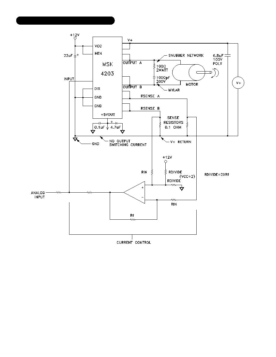
This is a diagram of a typical application of the MSK 4203. The design Vcc voltage is +12 volts and should have a good low
ESR bypass capacitor such as a tantalum. The analog input can be an analog speed control voltage from a potentiometer, other
analog circuitry or by microprocessor and a D/A converter. This analog input gets pulled by the current control circuitry in the proper
direction to reduce the current flow in the bridge if it gets too high. The gain of the current control amplifier will have to be set to
obtain the proper amount of current limiting required by the system.
Current sensing is done in this case by a 0.1 ohm sense resistor to sense current from both legs of the bridge separately. It is
important to make the high current traces as big as possible to keep inductance down. The storage capacitor connected to the V+
and the hybrid should be large enough to provide the high energy pulse without the voltage sagging too far. A low ESR ceramic
capacitor or large polypropylene capacitor will be required. Mount capacitor as close to hybrid as possible. The connection between
GND and the V+ return should not be carrying any motor current. The sense resistor signal is common mode filtered as necessary
to feed the limiting circuitry for the microprocessor. This application will allow full four quadrant torque control for a closed loop
servo system.
A snubber network is usually required, due to the inductance in the power loop. It is important to design the snubber network to
suppress any positive spikes above 75V and negative spikes below -2V with respect to GROUND.
TYPICAL SYSTEM OPERATION
Rev. A 10/02
4

The information contained herein is believed to be accurate at the time of printing. MSK reserves the right to make
changes to its products or specifications without notice, however, and assumes no liability for the use of its products.
Please visit our website for the most recent revision of this datasheet.
MECHANICAL SPECIFICATIONS
M.S. Kennedy Corp.
4707 Dey Road, Liverpool, N.Y. 13088
Phone (315) 701-6751
FAX (315) 701-6752
www.mskennedy.com
Rev. A 10/02
5
ALL DIMENSIONS ARE ±0.01 INCHES UNLESS OTHERWISE LABELED
ORDERING INFORMATION
MSK4203 H U
The above example is a Military grade class H hybrid with leads bent up.
LEAD CONFIGURATIONS
S= STRAIGHT; U= BENT UP; D= BENT DOWN
SCREENING
BLANK= INDUSTRIAL; E=EXTENDED RELIABILITY
H=MIL-PRF-38534 CLASS H
GENERAL PART NUMBER
ESD Triangle indicates Pin 1.