4707 Dey Road Liverpool, N.Y. 13088
(315) 701-6751
M.S.KENNEDY CORP.
ISO 9001 CERTIFIED BY DSCC
75 VOLT 6 AMP MOSFET
H-BRIDGE PWM MOTOR
DRIVER/AMPLIFIER
4223
FEATURES:
Low Cost Complete H-Bridge
6 Amp Capability, 75 Volt Maximum Rating
Self-contained Smart Lowside/Highside Drive Circuitry
Internal PWM Generation, Shoot-through Protection
Isolated Case Allows Direct Heatsinking
Four Quadrant Operation, Torque Control Capability
Logic Level Disable Input
Logic Level High Side Enable Input for Special Modulation or Function
Available With Leads Bent Up Or Down
DESCRIPTION:
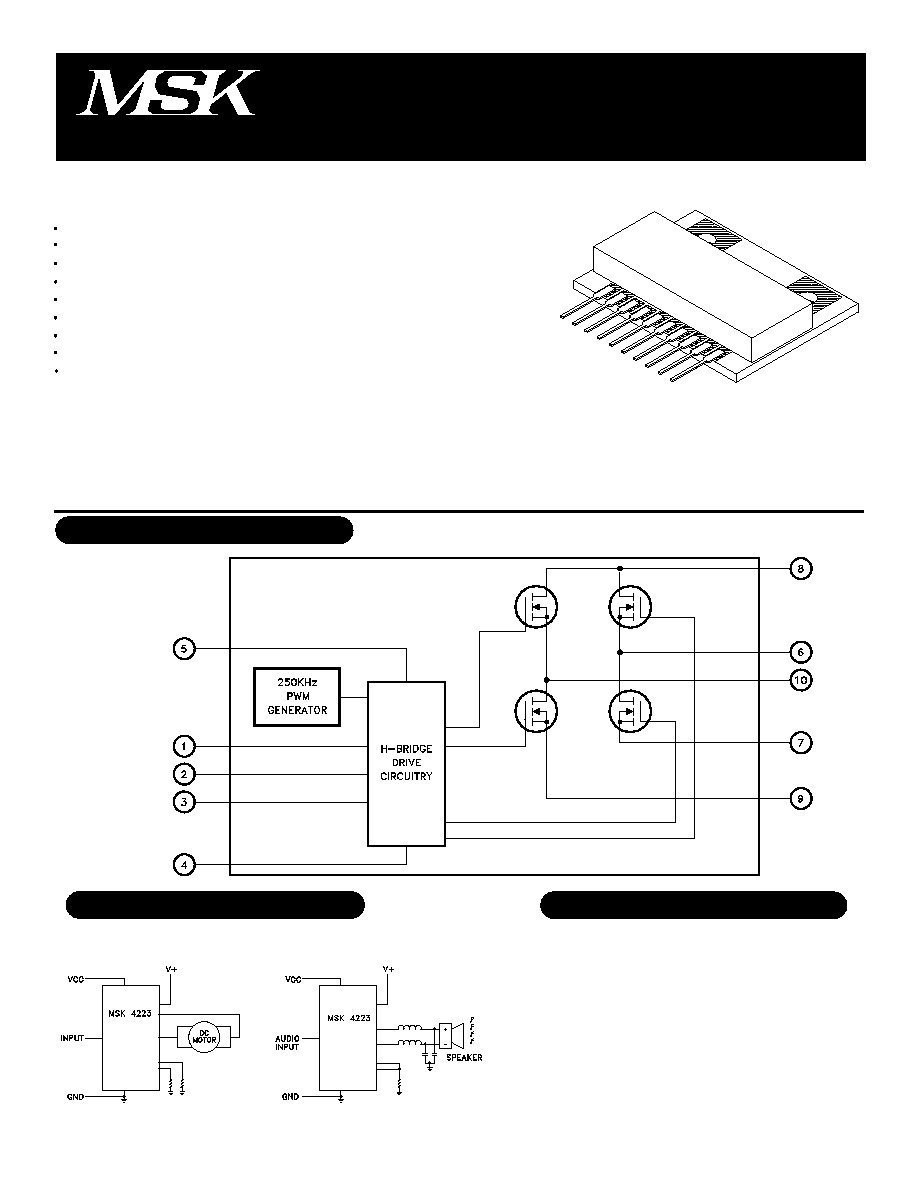
The MSK 4223 is a complete H-Bridge circuit to be used for DC brushed motor control or Class D switchmode
amplification. All of the drive/control circuitry for the lowside and highside switches are internal to the circuit. The
PWM circuitry is internal as well, leaving the user to only provide an analog signal for the motor speed/direction, or
audio signal for switchmode audio amplification. The MSK 4223 is constructed on a space efficient ceramic sub-
strate that can be directly connected to a heatsink.
EQUIVALENT SCHEMATIC
TYPICAL APPLICATIONS
PIN-OUT INFORMATION
1
2
3
4
5
6
7
8
9
10
HEN
Disable
Input
Ground
Vcc
Output A
Rsense A
V+
Rsense B
Output B
PRELIMINARY Rev. F 10/00
1
75V
16V
6A
9A
GND-2V min. To V+ max.
4.6∞C/W
OUTPUT CHARACTERISTICS
VDS(ON) Voltage
Instantaneous Forward Voltage
Reverse Recovery Time
Leakage Current
PWM Frequency
Vcc SUPPLY CHARACTERISTICS
Quiescent Bias Current
Vcc Voltage Range
INPUT SIGNAL CHARACTERISTICS
Analog Input Voltage
Analog Input Voltage
Analog Input Voltage
LOGIC CONTROL INPUTS
SWITCHING CHARACTERISTICS
Rise-Time
Fall-Time
Dead-Time
High Voltage Supply
Logic Supply
Continuous Output Current
Peak Output Current
Output Voltage Range
Thermal Resistance
(Output Switches)
ABSOLUTE MAXIMUM RATINGS
V+
V
CC
I
OUT
I
PK
V
OUT
JC
-65∞C to +150∞C
300∞C
-40∞C to +125∞C
+150∞C
Storage Temperature Range
Lead Temperature Range
(10 Seconds)
Case Operating Temperature
MSK4223
Junction Temperature
T
ST
T
LD
T
C
T
J
1
2
NOTES:
Disable Input
HEN Input
Each MOSFET I
D
=6A
Each MOSFET I
S
=6A Intrinsic Diode
Intrinsic Diode
Each MOSFET V+=70V
Analog Input=6V
DC
R
L
=
Output A,B=50% Duty Cycle
Output A=100% Duty Cycle High
Output B=100% Duty Cycle High
Input Voltage LO
Input Voltage HI
Input Current (DISABLE=0V)
Input Voltage LO
Input Voltage HI
Input Current (HEN=0V)
R
L
=100
V+=75V
V+=75V
Parameter
ELECTRICAL SPECIFICATIONS
Units
V
V
nS
uA
KHz
mA
V
V
V
V
V
V
uA
V
V
uA
nS
nS
nS
All Ratings: Tc= +25∞C Unless Otherwise Specified
1
1
1
1
Max.
1.5
1.8
260
25
275
60
16
6.5
3.5
9.5
0.8
-
-135
0.8
-
-270
84
50
-
MSK 4223
Typ.
0.75
1.1
-
1.0
250
46
12
6
3
9
-
-
-
-
-
-
56
33
100
Min.
-
-
-
-
225
-
9
5.5
2.5
8.5
-
2.7
-
-
2.7
-
-
-
-
Test Conditions
2
1
2
Guaranteed by design but not tested. Typical parameters are representative of actual device performance but are for reference only.
Vcc=+12V, V+=28V, R
L
=1K A
OUT
to B
OUT
, unless otherwise specified.
PRELIMINARY Rev. F 10/00
1
1
APPLICATION NOTES
IN
VCC - Is the low voltage supply for powering internal
logic and drivers for the lowside and highside MOSFETS.
The supplies for the highside drivers are derived from
this voltage.
OUTPUT B - Is the output pin for the other half of the
bridge. Increasing the input voltage causes increasing
duty cycles at this output.
OUTPUT A - Is the output pin for one half of the bridge.
Decreasing the input voltage causes increasing duty
cycles at this output.
RSENSE A - Is the connection for the bottom of the A
half bridge. This can have a sense resistor connection
to the V+ return ground for current limit sensing, or
can be connected directly to ground. The maximum
voltage on this pin is ±2 volts with respect to GND.
RSENSE B - Is the connection for the bottom of the B
half bridge. This can have a sense resistor connection
to the V+ return ground for current limit sensing, or
can be connected directly to ground. The maximum
voltage on this pin is ±2 volts with respect to GND.
GND - Is the return connection for the input logic and
Vcc.
INPUT - Is an analog input for controlling the PWM
pulse width of the bridge. A voltage lower than Vcc/2
will produce greater than 50% duty cycle pulses out of
OUTPUT A. A voltage higher than Vcc/2 will produce
greater than 50% duty cycle pulses out of OUTPUT B.
DISABLE - Is the connection for disabling all 4 output
switches. DISABLE high overrides all other inputs.
When taken low, everything functions normally. An
internal pullup to Vcc will keep DISABLE high if left
unconnected.
HEN - Is the connection for enabling the high side out-
put switches. When taken low, HEN overrides other
inputs and the high side switches remain off. When
HEN is high everything functions normally. An internal
pullup to Vcc will keep HEN high if left unconnected.
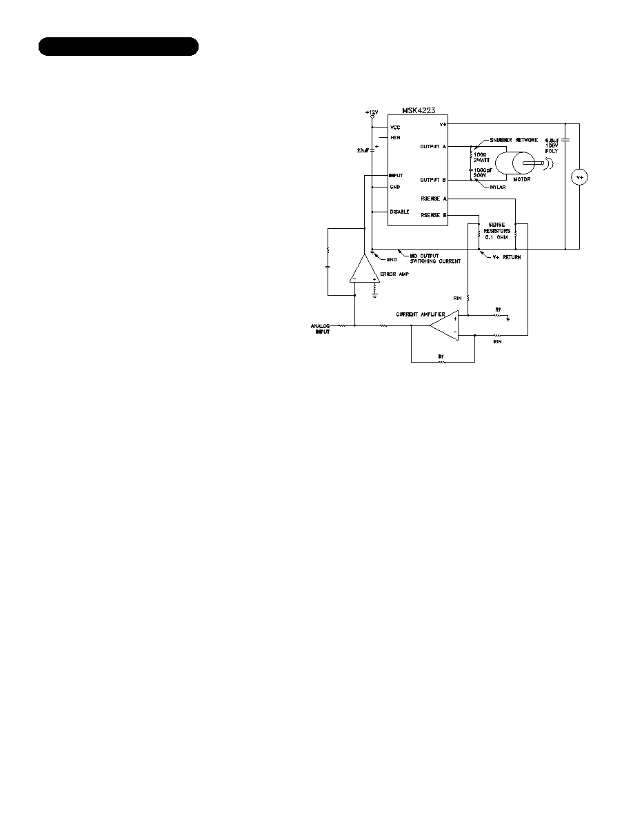
This is a diagram of a typical application of the MSK 4223.
The design Vcc voltage is +12 volts and should have a good
low ESR bypass capacitor such as a tantalum electrolytic.
The analog input can be an analog speed control voltage from
a potentiometer, other analog circuitry or by microprocessor
and a D/A converter. This analog input gets pulled by the
current control circuitry in the proper direction to reduce the
current flow in the bridge if it gets too high. The gain of the
current control amplifier will have to be set to obtain the
proper amount of current limiting required by the system.
Current sensing is done in this case by a 0.1 ohm sense
resistor to sense current from both legs of the bridge sepa-
rately. It is important to make the high current traces as big
as possible to keep inductance down. The storage capacitor
connected to the V+ and the module should be large enough
to provide the high energy pulse without the voltage sagging
too far. A low ESR ceramic capacitor or large polypropylene
capacitor will be required. Mount the capacitor as close to
the module as possible. The connection between GND and
the V+ return should not be carrying any motor current. The
sense resistor signal is common mode filtered as necessary
to feed the limiting circuitry for the microprocessor. This
application will allow full four quadrant torque control for a
closed loop servo system.
A snubber network is usually required, due to the induc-
tance in the power loop. It is important to design the snub-
ber network to suppress any positive spikes above 75V and
negative spikes below -2V with respect to ground.
V+ - Is the higher voltage H-bridge supply. The
MOSFETS obtain the drive current from this supply pin.
The voltage on this pin is limited by the drive IC. The
MOSFETS are rated at 100 volts. Proper by-passing to
GND with sufficient capacitance to suppress any volt-
age transients, and to ensure removing any drooping
during switching, should be done as close to the pins
of the module as possible.
MSK 4223 PIN DESCRIPTIONS
TYPICAL SYSTEM OPERATION
3
PRELIMINARY Rev. F 10/00