 | –≠–ª–µ–∫—Ç—Ä–æ–Ω–Ω—ã–π –∫–æ–º–ø–æ–Ω–µ–Ω—Ç: MSK4227G | –°–∫–∞—á–∞—Ç—å:  PDF PDF  ZIP ZIP |
20
19
18
17
16
15
14
13
12
11
4707 Dey Road Liverpool, N.Y. 13088
(315) 701-6751
M.S.KENNEDY CORP.
ISO 9001 CERTIFIED BY DSCC
200 VOLT 20 AMP MOSFET
H-BRIDGE WITH
GATE DRIVE
4227
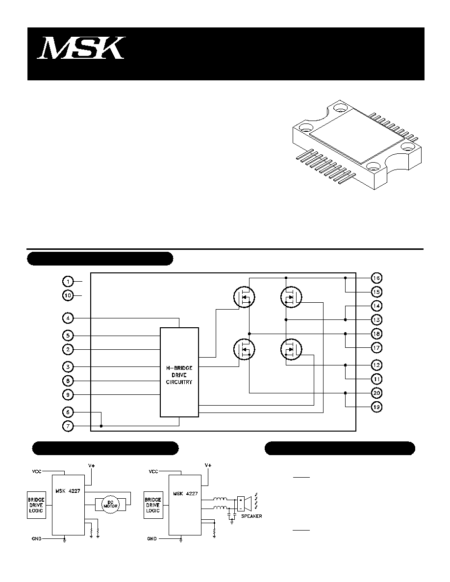
The MSK 4227 is a complete H-Bridge circuit to be used for DC brushed motor control or Class D switchmode amplifi-
cation. All of the drive/control circuitry for the lowside and highside switches are internal to the circuit. Logic level inputs
are provided for controlling each MOSFET independently, allowing every possible switch combination except those that
would cause a simultaneous conduction or shoot-through condition for each half bridge. This gives the user freedom to use
various modulation schemes for PWM control. The MSK 4227 is constructed in a space efficient plastic power package
that can be directly bolted to a heatsink.
DESCRIPTION:
EQUIVALENT SCHEMATIC
TYPICAL APPLICATIONS
PIN-OUT INFORMATION
1
2
3
4
5
6
7
8
9
10
Rev. B 11/04
1
FEATURES:
∑
Low Cost Complete H-Bridge
∑
20 Amp Capability, 200 Volt Maximum Rating
∑
Self-contained Smart Lowside/Highside Drive Circuitry
∑
Shoot-through Protection
∑
Isolated Case Allows Direct Heatsinking
∑
Logic Level Disable Input
∑
Individual Logic Level Gate Drive Inputs for Various Modulation Schemes
NC
HINA
LINA
+VCC
+VB
COM
COM
HINB
LINB
NC
AV-
AV-
Aÿ
Aÿ
V+
V+
Bÿ
Bÿ
BV-
BV-

Each MOSFET I
D
=20A
Each MOSFET I
D
=20A 3
Each MOSFET I
S
=20A Intrinsic Diode 3
Intrinsic Diode
Each MOSFET V+=200V
R
L
=100
OUTPUT CHARACTERISTICS
RDS (ON) 1 4
VDS(ON) Voltage
Instantaneous Forward Voltage
Reverse Recovery Time 1
Leakage Current
+Vcc SUPPLY CHARACTERISTICS
Quiescent Bias Current
Vcc Voltage Range 1
+VB SUPPLY CHARACTERISTICS
Quiescent Bias Current
Bias Current @ 20KHz
+VB Voltage Range
LOGIC CONTROL INPUTS, HINA, LINA, HINB, LINB 1
Input Voltage LO
Input Voltage HI
Input Current (V
IN
=5V)
SWITCHING CHARACTERISTICS 1
Rise Time
Fall Time
Dead Time
V+
V
CC
I
OUT
I
PK
JC
ABSOLUTE MAXIMUM RATINGS
Parameter
ELECTRICAL SPECIFICATIONS
Units
V
V
nS
µA
mA
V
µA
mA
V
V
V
µA
nS
nS
µS
Max.
0.09
1.8
1.2
330
250
3.2
18
300
6
18
0.8
-
20
-
-
-
MSK 4227
Typ.
-
1.2
1.02
-
3.0
0.9
15
100
4
15
-
-
-
90
100
1
Min.
-
-
-
-
-
-
7.4
-
-
9.8
-
2.7
-
-
-
-
Test Conditions 2
2
T
ST
T
LD
T
C
T
J
NOTES:
1
Guaranteed by design but not tested. Typical parameters are representative of actual device performance but are for reference only.
2
+Vcc=+15V, +VB=+15V, V+=100V, AV-, BV- = Ground unless otherwise specified.
3
Measured using a 300µS pulse with a 2% Duty Cycle.
4
On Resistance is specified for the Internal MOSFET for Thermal Calculations. It does not include the package pin resistance.
Tc= +25∞C Unless Otherwise Specified
Rev. B 11/04
High Voltage Supply
Logic Supply
Continuous Output Current
Peak Output Current
Thermal Resistance
(Output Switches @ 125∞C)
200V
18V
20A
44A
2.3∞C/W
Storage Temperature Range
Lead Temperature Range
(10 Seconds)
Case Operating Temperature
MSK4227
Junction Temperature
-55∞C to +125∞C
300∞C
-40∞C to +85∞C
+150∞C
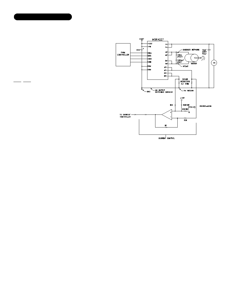
APPLICATION NOTES
IN
+VCC - Is the low voltage supply for all the internal logic and
drivers. A 0.1µF ceramic capacitor in parallel with a 10µF
tantalum capacitor is the recommended bypassing from the
+VCC pin to the COM pin.
LINA, LINB - Are low active logic inputs for signaling the cor-
responding phase low-side switch to turn on. The logic in-
puts are compatible with standard CMOS or LSTTL outputs.
These logic numbers are internally zener clamped at 5.2 volts.
Aÿ, Bÿ - Are the pins connecting the 3 phase bridge switch
options.
AV-, BV- - Are the connections from the bottoms of the three
half bridges. These pins get connected to the COM pin. If
current sensing is desired they may be connected to the COM
pin through a low value sense resistor.
+VB - Is the connection used to provide power to the floating
high-side bootstrap supplies in the gate drive circuitry.
This is a diagram of a typical application of the MSK4227.
The design +Vcc voltage is +15 volts and should have a
good low ESR bypass capacitor such as a tantalum electro-
lytic. The digital inputs can come from a microprocessor or
any type of PWM controller. The controller will use the cur-
rent sense signal to either control current through PWM, cur-
rent limit the bridge, or both.
Current sensing is done in this case by a 0.1 ohm sense
resistor to sense current from both legs of the bridge sepa-
rately. It is important to make the high current traces as big as
possible to keep inductance down. The storage capacitor con-
nected to the V+ and the module should be large enough to
provide the high energy pulse without the voltage sagging
too far. A low ESR ceramic capacitor or large polypropylene
capacitor will be required. Mount the capacitor as close to the
module as possible. The connection between GND and the
V+ return should not be carrying any motor current. The
sense resistor signal is common mode filtered as necessary to
feed the limiting circuitry for the microprocessor. This appli-
cation will allow full four quadrant torque control for a closed
loop servo system. Any modulation scheme may be used,
however, but the current sensing scheme may have to change.
A snubber network is usually required, due to the induc-
tance in the power loop. It is important to design the snubber
network to suppress any positive spikes above 200V and
negative spikes below -2V with respect to ground.
HINA, HINB - Are high active logic inputs for signaling the
corresponding phase high-side switch to turn on. The logic
inputs are compatible with standard CMOS or LSTTL outputs.
These logic numbers are internally zener clamped at 5.2 volts.
MSK 4227 PIN DESCRIPTIONS
TYPICAL SYSTEM OPERATION
3
Rev. B 11/04
V+ - Is the high voltage positive rail connection to the tops of
the three half bridges. Proper power supply bypassing must
be connected from this pin to the COM pin for good filtering.
This bypassing must be done as close to the hybrid as pos-
sible.
COM - Is the connection that all hybrid power supply connec-
tions are returned to and bypassed to.

The information contained herein is believed to be accurate at the time of printing. MSK reserves the right to make
changes to its products or specifications without notice, however, and assumes no liability for the use of its products.
Please visit our website for the most recent revision of this datasheet.
MECHANICAL SPECIFICATIONS
M.S. Kennedy Corp.
4704 Dey Road, Liverpool, New York 13088
Phone (315) 701-6751
FAX (315) 701-6752
www.mskennedy.com
Screening
Level
Part
Number
MSK4227S
MSK4227D
MSK4227U
MSK4227G
Industrial
Industrial
Industrial
Industrial
ORDERING INFORMATION
NOTE: ALL DIMENSIONS ARE ±0.010 UNLESS OTHERWISE LABELED.
ESD Triangle Indicates Pin 1.
4
Rev. B 11/04
Lead
Configuration
Straight
Down
Up
Gull Wing