 | –≠–ª–µ–∫—Ç—Ä–æ–Ω–Ω—ã–π –∫–æ–º–ø–æ–Ω–µ–Ω—Ç: MSK4310 | –°–∫–∞—á–∞—Ç—å:  PDF PDF  ZIP ZIP |
4707 Dey Road Liverpool, N.Y. 13088
(315) 701-6751
M.S.KENNEDY CORP.
ISO 9001 CERTIFIED BY DSCC
4310
10 AMP, 55V, 3 PHASE
BRUSHLESS MOTOR
SPEED CONTROLLER
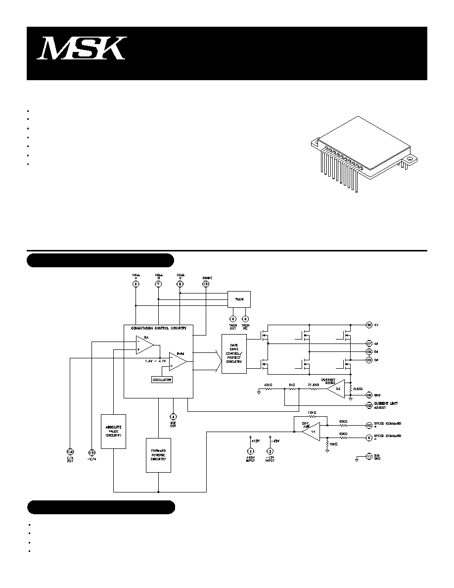
EQUIVALENT SCHEMATIC
DESCRIPTION:
The MSK 4310 is a complete 3 Phase Brushless Motor Speed Controller in an electrically isolated hermetic
package. The hybrid is capable of 10 amps of output current and 55 volts of DC bus voltage. Included is all of the
bridge drive circuitry, hall sensing circuitry and commutation circuitry. Also included is a user programable current
limit circuit and a tachometer circuit for closed loop operation. The MSK 4310 has good thermal conductivity of the
output switches due to isolated substrate/package design that allows direct heat sinking of the hybrid without
insulators.
FEATURES:
55 Volt Motor Supply Voltage
10 Amp Output Switch Capability
Shoot-Through/Cross Conduction Protection
Hall Sensing and Commutation Circuitry on Board
User Programable Current Limit
Tach Out-Closed Loop Control
Available With 3 Lead Configurations
TYPICAL APPLICATIONS
Fan/Blower Speed Control
Azimuth/Elevation Antenna Control
Optical Tracking Control
Robot Velocity Control
MIL-PRF-38534 QUALIFIED
Rev. A 2/03
1
+55V
±15VIN
+V REF
10A
15A
+16V
-16V
High Voltage Supply
Speed Command (+,-)
Hall A,B,C,Brake
Continuous Output Current
Peak Output Current
+15 Volt Input Voltage
-15 Volt Input Voltage
ABSOLUTE MAXIMUM RATINGS
V+
V
IN
I
OUT
I
pK
+15V
IN
-15V
IN
4.8∞C/W
-65∞C to +150∞C
+300∞C
-40∞C to +85∞C
-55∞C to +125∞C
+150∞C
O
JC
T
ST
T
LD
T
C
T
J
Thermal Resistance (@ 125∞C)
Storage Temperature Range
Lead Temperature Range
(10 Seconds)
Case Operating Temperature
MSK4310
MSK4310H/E
Junction Temperature
Rev. A 2/03
2
±15V INPUT=±15V, V+=28V, BRAKE=GND unless otherwise specified.
Guaranteed by design but not tested. Typical parameters are representative of actual device performance but are for reference only.
Industrial grade and "E" suffix devices shall be tested to subgroups 1 and 4 unless otherwise specified.
Military grade devices ("H" Suffix) shall be 100% tested to Subgroups 1, 2, 3 and 4.
Subgroups 5 and 6 testing available upon request.
Subgroup 1, 4 TA
= TC = +25∞C
2, 5 TA
= TC =+125∞C
3, 6 TA
= TC =
-55∞C
4
5,6
1
2,3
1
2,3
-
-
1
1
-
1
2,3
-
-
-
-
-
-
-
-
-
-
-
-
-
-
-
4
1,2,3
PWM
POWER SUPPLY REQUIREMENTS
HALL INPUTS
VIL
VIH
ANALOG SECTION
Speed Command Input Range
Speed Command Input Range
Speed Command Input Current
REFERENCE OUTPUT VOLTAGE
ERROR AMP
Input Offset Voltage
Input Offset Current
Input Bias Current
Input Common Mode Voltage Range
Open-Loop Voltage Gain
Input Common Mode Rejection Ratio
Power Supply Rejection Ratio
OUTPUT SECTION
Voltage Drop Across Bridge (1 Upper & 1 Lower)
Voltage Drop Across Bridge (1 Upper & 1 Lower)
Leakage Current
Diode VSD
trr
Dead Time
TACH OUT
Output Voltage High State
Output Voltage Low State
Output Pulse Width
CURRENT LIMIT
Current Limit
E/A DC Gain=1, Positive Command
E/A DC Gain=1, Negative Command
V
IN
=5V
V
O=
3V, R
L=
15K
10 AMPS
10 AMPS @ 150∞C Junction
All switches off, V+=44V, 150∞C Junction
I Source = 5mA
I Sink = 10mA
R/C=20K/0.01uF
Current Limit Adjust Pin=Open
ELECTRICAL SPECIFICATIONS
Parameter
Units
MSK 4310
Test Conditions
KHz
KHz
mA
mA
mA
mA
VOLTS
VOLTS
VOLTS
VOLTS
mA
VOLTS
VOLTS
mV
nA
nA
V
db
db
db
VOLTS
VOLTS
µA
VOLTS
nSec
µSec
V
V
µSec
Amps
Min.
Typ.
Max.
MSK 4310H/E
Min.
Typ.
Max.
Group A
Subgroup
21
20
-
-
-
-
-
3.0
1.2
-1.2
-
5.9
5.82
-
-
-
0
70
55
65
-
-
-
-
-
-
3.60
-
150
0.4
25
25
37
41
8
9
-
-
-
-
-
6.24
-
0.4
8.0
-46
-
80
86
105
0.8
1.6
-
-
86
2
3.95
0.25
200
1
29
30
50
60
15
20
0.8
-
4.5
-4.5
1.5
6.5
6.57
10
500
-1000
V
REF
-
-
-
-
1.92
750
1.6
-
-
4.20
0.50
250
1.60
20
-
-
-
-
-
-
3.0
1.2
-1.2
-
5.82
-
-
-
-
0
70
55
65
-
-
-
-
-
-
3.60
-
150
0.3
25
-
37
-
8
-
-
-
-
-
-
6.24
-
0.4
8.0
-46
-
80
86
105
0.8
1.6
-
-
86
2
3.95
0.25
200
1
30
-
60
-
18
-
0.8
-
4.5
-4.5
1.5
6.57
-
10
500
-1000
V
REF
-
-
-
-
1.92
750
1.6
-
-
4.20
0.50
250
1.70
3
3
Clock Frequency
NOTES:
@ 1mA
1
2
3
4
5
6
V
IND
+15 Volt Input Current
-15 Volt Input Current
Reference Voltage
2
2
2
2
2
2
2
2
2
2
2
2
2
2
2
1
2

APPLICATION NOTES
MSK 4310 PIN DESCRIPTIONS
V+ - is the power connection from the hybrid to the
bus. The external wiring to the pin should be sized
according to the RMS current required by the motor.
This pin should be bypassed by a high quality mono-
lithic ceramic capacitor for high frequencies and enough
bulk capacitance to keep the V+ power supply from
drooping.
Aÿ OUT, Bÿ OUT, Cÿ OUT-are the connections to the
motor phase windings from the bridge output. The wir-
ing to these pins should be sized according to the mo-
tor current requirements. There are no internal short
circuit protection provisions for these output pins in
the hybrid. Shorts to V+ or ground from these pins
must be avoided or the bridge will be destroyed.
GND- is the power return connection from the hybrid
to the bus. All ground returns internal to the hybrid
connect to this point in a star configuration. All exter-
nal ground connections to this point should be made in
a similar fashion. The V+ capacitors should be returned
to this pin as close as possible. Wire sizing to this pin
connection should be made according to the required
current.
SIG GND - is the ground pin that connects to the ground
plane for all low power circuitry inside the device.
+15 V INPUT - is the pin for applying +15 volts to run
the low power control circuitry inside the hybbrid. This
pin should be bypassed to the signal ground pin using
a high quality 10µF tantalum capacitor and a 0.1µF
ceramic capacitor as close to these pins as possible.
-15 V INPUT - is the pin for applying -15 volts to run
the low power control circuitry inside the hybrid. This
pin should be bypassed to the signal ground pin using
a high quality 10µF tantalum capacitor and a 0.1µF
ceramic capacitor as close to these pins as possible.
BRAKE - is the pin for commanding the output bridge
into a motor brake mode. When this pin is taken low,
normal operation of the hybrid proceeds. When this
pin is taken high, the three high side switches in the
bridge turn off and the three lowside switches turn
fully on. This will cause rapid deceleration of the motor
and will cease motor operation until taken low again.
The pin left open is internally pulled high.
3
Rev. A 2/03
HALL A, B & C - are the hall input pins from the hall
devices in the motor. These pins are internally pulled
up to 6.25 volts. The halls reflect a 120/240 degree
commutation scheme.
TACH RC - is used to set the tach out pulse width.
This is done by connecting a resistor from this pin to
the REF OUT pin and a capacitor from the pin to the
signal ground. Selection of these components is based
on the desired maximum motor speed. (See TACH RC
component selection)
TACH OUT - is connected to the -E/A pin through a
resistor when using the speed controller in a closed
loop configuration..
-E/A - is the error amp inverting input connection. It is
brought out to allow various loop compensation cir-
cuits to be connected between this and E/A out.
E/A OUT - this is the loop error amp output connec-
tion. It is brought out for allowing various loop com-
pensation circuits to be connected between this and
-E/A.
REF OUT - is a 6.25 volt regulated output that can be
used to power the hall devices in various motors. Up
to 15 milliamps of current is available.
CURRENT LIMIT ADJUST - is used to adjust the out-
put current limit. The pin, if left open will limit the
output current to about 1 amp. The pin, taken to ground
will limit the current to about 15 amps. A resistor from
the pin to ground will yield current limits in between.
(See Current Limit Adjust)
SPEED COMMAND (+,-) - are differential inputs for
controlling the motor speed. With a positive voltage
command the motor will operate in the forward direc-
tion and with a negative command the motor will op-
erate in the reverse direction. The maximum opera-
tional command voltage should be ±5 volts.

1
=
High Level
H
=
SOURCE
0
=
Low Level
L
=
SINK
X
=
Don't Care
-
=
OPEN
COMMUTATION TRUTH TABLE
HALL SENSOR PHASING
SPEED
COMMAND
= POS.
SPEED
COMMAND
= NEG.
120∞
HALL
A
1
1
0
0
0
1
1
0
X
HALL
B
0
1
1
1
0
0
1
0
X
HALL
C
0
0
0
1
1
1
1
0
X
Aÿ
H
-
L
L
-
H
-
-
L
Bÿ
-
H
H
-
L
L
-
-
L
Cÿ
L
L
-
H
H
-
-
-
L
Aÿ
L
-
H
H
-
L
-
-
L
Bÿ
-
L
L
-
H
H
-
-
L
Cÿ
H
H
-
L
L
-
-
-
L
4
Rev. A 2/03
APPLICATION NOTES CONTINUED
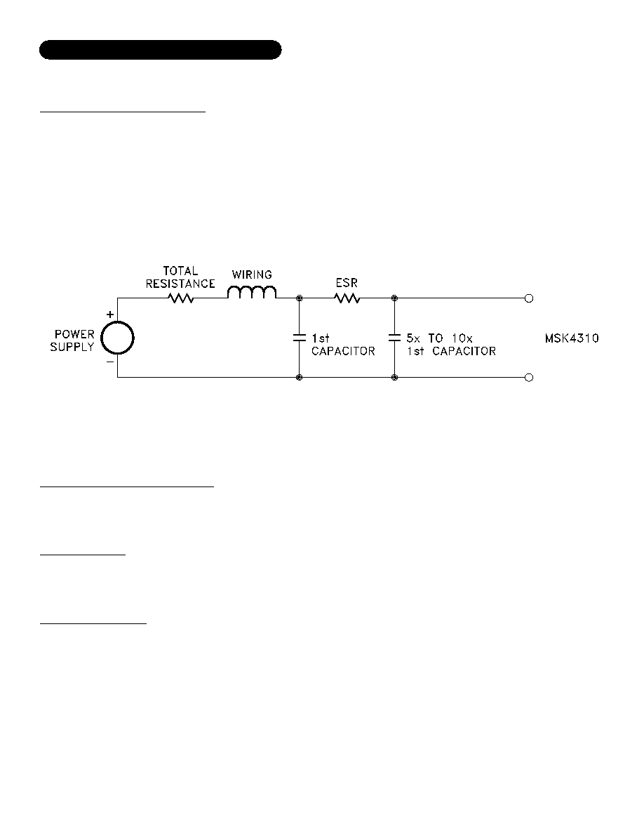
BUS VOLTAGE FILTER CAPACITORS
The size and placement of the capacitors for the DC bus has a direct bearing on the amount of noise filtered and also on the size
and duration of the voltage spikes seen by the bridge. What is being created is a series RLC tuned circuit with a resonant
frequency that is seen as a damped ringing every time one of the transistors switches. For the resistance, wire resistance, power
supply impedance and capacitor ESR all add up for the equivalent lumped resistance in the circuit. The inductance can be figured
at about 30 nH per inch from the power supply. Any voltage spikes are on top of the bus voltage and the back EMF from the
motor. All this must be taken into account when designing and laying out the system. If everything has been minimized, there is
another solution. A second capacitance between 5 and 10 times the first capacitor and it should either have some ESR or a
resistor can be added in series with the second capacitor to help damp the voltage spikes.
Be careful of the ripple current in all the capacitors. Excessive ripple current, beyond what the capacitors can handle, will destroy
the capacitors.
INPUT VOLTAGE FILTER CAPACITORS
It is recommended that about 10 µF of capacitance (tantalum electrolytic) for bypassing the + and -15V power supplies be placed
as close to the module pins as practical. Adding ceramic bypass capacitors of about 0.1 µF to 1 µF will aid in suppressing noise
transients.
GENERAL LAYOUT
Good PC layout techniques are a must. Ground plane for the analog circuitry must be used and should be tied back to the SIG
GND. Ground plane for the power circuitry should be tied back to the GND pin, pin 16. Pin 16 should be connected to pin 11
external to the hybrid by a single thick trace. This will connect the two ground planes together.
LOW POWER STARTUP
When starting up a system utilizing the MSK 4310 for the first time, there are a few things to keep in mind. First, because of the
small size of the module, short circuiting the output phases either to ground or the DC bus will destroy the bridge. The current
limiting and control only works for current actually flowing through the bridge. The current sense resistor has to see the current
in order for the electronics to control it. If possible, for startup use a lower voltage and lower current power supply to test out
connections and the low current stability. With a limited current supply, even if the controller locks up, the dissipation will be
limited. The ±15 volt power should be applied prior to applying the V+ voltage.
5
Rev. A 2/03
APPLICATION NOTES CONTINUED