 | –≠–ª–µ–∫—Ç—Ä–æ–Ω–Ω—ã–π –∫–æ–º–ø–æ–Ω–µ–Ω—Ç: MSK4360HD | –°–∫–∞—á–∞—Ç—å:  PDF PDF  ZIP ZIP |

4707 Dey Road Liverpool, N.Y. 13088
(315) 701-6751
M.S.KENNEDY CORP.
ISO 9001 CERTIFIED BY DSCC
4360
10 AMP, 55V, 3 PHASE
MOSFET BRUSHLESS
MOTOR CONTROLLER
EQUIVALENT SCHEMATIC
DESCRIPTION:
The MSK 4360 is a complete 3 Phase MOSFET Bridge Brushless Motor Control System in an electrically isolated
hermetic package. The hybrid is capable of 10 amps of output current and 55 volts of DC bus voltage. It has the
normal features for protecting the bridge. Included is all the bridge drive circuitry, hall sensing circuitry, commutation
circuitry and all the current sensing and analog circuitry necessary for closed loop current mode (torque) control.
When PWM'ing, the transistors are modulated in locked anti-phase mode for the tightest control and the most
bandwidth. Provisions for applying different compensation schemes are included. The MSK 4360 has good thermal
conductivity of the MOSFET's due to isolated substrate/package design that allows direct heat sinking of the hybrid
without insulators.
FEATURES:
55 Volt Motor Supply Voltage
10 Amp Output Switch Capability
100% Duty Cycle High Side Conduction Capable
Shoot-Through/Cross Conduction Protection
Hall Sensing and Commutation Circuitry on Board
Internal ±15 Volt Regulators
"Real" Four Quadrant Torque Control Capability
Good Accuracy Around the Null Torque Point
Isolated Package for High Voltage Isolation Plus Good Thermal Transfer
TYPICAL APPLICATIONS
3 Phase Brushless DC Motor Control
Servo Control
Fin Actuator Control
MIL-PRF-38534 QUALIFIED
Rev. G 11/01
1
Gimbal Control
AZ-EL Control
55V
0.16A
±13.5V
20mA
20mA
10A
16A
High Voltage Supply
V+ Quiescent Current
Current Command Input
Output Current
Output Current
Continuous Output Current
Peak Output Current
ABSOLUTE MAXIMUM RATINGS
V+
I
Q
V
IN
+15V
-15V
I
OUT
I
PK
3.6∞C/W
-65∞C to +150∞C
+300∞C
-40∞C to +85∞C
-55∞C to +125∞C
+150∞C
O
JC
T
ST
T
LD
T
C
T
J
Thermal Resistance
Storage Temperature Range
Lead Temperature Range
(10 Seconds)
Case Operating Temperature
MSK4360
MSK4360H/E
Junction Temperature
Rev. G 11/01
2
Guaranteed by design but not tested. Typical parameters are representative of actual device performance but are for reference only.
Industrial grade and "E" suffix devices shall be tested to subgroups 1 and 4 unless otherwise specified.
Military grade devices ("H" Suffix) shall be 100% tested to Subgroups 1, 2, 3 and 4.
Subgroups 5 and 6 testing available upon request.
Subgroup 1, 4 TA = TC = +25∞C
2, 5 TA = TC =+125∞C
3, 6 TA = TC = -55∞C
Maximum power dissipation must be limited according to voltage regulator power dissipation.
Measurements do not include offset current at 0V current command.
4
5,6
1,2,3
1,2,3
4
-
-
-
-
4
5,6
1
2,3
4
5,6
-
-
-
-
-
-
-
-
-
-
PWM
REGULATORS
+15 VOUT
-15 VOUT
-15 VOUT Ripple
HALL INPUTS
VIL
VIH
ANALOG SECTION
Current Command Input Range
Current Command Input Current
Current Monitor Voltage Swing
ERROR AMP
E/A OUTPUT Swing
Slew Rate
Unity Gain Bandwidth
Large Signal Voltage Gain
OUTPUT SECTION
Voltage Drop Across Bridge (1 Upper & 1 Lower)
Voltage Drop Across Bridge (1 Upper & 1 Lower)
Leakage Current
Diode VSD
trr
Dead Time
20mA Load
20mA Load
20mA Load
5mA Load
5mA Load
10 AMPS
10 AMPS @ 150∞c Junction
All switches off, V+=44V, 150∞C Junction
ELECTRICAL SPECIFICATIONS
Parameter
Units
MSK 4360
Test Conditions
KHz
KHz
VOLTS
VOLTS
mV
VOLTS
VOLTS
VOLTS
mA
A/V
A/V
mA
mA
V/A
V/A
VOLTS
VOLTS
V/µSec
MHz
V/mV
VOLTS
VOLTS
µA
VOLTS
nSec
µSec
Min.
Typ.
Max.
MSK 4360H/E
Min.
Typ.
Max.
Group A
Subgroup
15
13.6
14.25
-15.75
-
-
3.0
-13.5
-
1.9
1.8
-25
-50
0.475
0.45
-12
-12
-
-
-
-
-
-
-
-
-
16
22
-
-
-
-
-
-
-
2
2
0
0
0.5
0.5
-
-
3
1.8
400
0.8
1.6
-
-
86
2
17
18.4
15.75
-14.25
250
0.8
-
+13.5
1.5
2.1
2.2
25
50
0.525
0.55
+12
+12
-
-
-
-
1.92
750
1.6
-
-
15
-
14.25
-15.75
-
-
3.0
-13.5
-
1.8
-
-50
-
0.45
-
-12
-12
-
-
-
-
-
-
-
-
-
16
-
-
-
-
-
-
-
-
2
-
0
-
0.5
-
-
-
3
1.8
400
0.8
1.6
-
-
86
2
17
-
15.75
-14.25
250
0.8
-
+13.5
1.5
2.2
-
50
-
0.55
-
+12
+12
-
-
-
-
1.92
750
1.6
-
-
1
1
1
1
1
1
1
1
1
1
1
1
1
1
6
1
3
6
2
Transconductance
Offset Current
Current Monitor
Clock Frequency
NOTES:
Current Command=0 Volts
7
7
@ ±1 Amp Output
1
2
3
4
5
6
7

APPLICATION NOTES
MSK 4360 PIN DESCRIPTIONS
V+ - is the power connection from the hybrid to the bus. The
external wiring to the pin should be sized according to the
RMS current required by the motor. The pin should be by-
passed by a high quality monolithic ceramic capacitor for high
frequencies and enough bulk capacitance for keeping the V+
supply from drooping. 78 µF of ceramic capacitance and
1700 µF of bulk capacitance was used in the test circuit.
The voltage range on the pin is from 16 volts up to 55 volts.
MOTOR DRIVE A,B,C - are the connections to the motor
phase windings from the bridge output. The wiring to these
pins should be sized according to the required current by the
motor. There are no short circuit provisions for these out-
puts. Shorts to V+ or V+ RTN from these pins must be
avoided or the bridge will be destroyed.
V+ RTN - is the power return connection from the module to
the bus. All ground returns connect to this point from inter-
nal to the module in a star fashion. All external ground con-
nections to this point should also be made in a similar fash-
ion. The V+ capacitors should be returned to this pin as
close as possible. Wire sizing to this pin connection should
be made according to the required current.
SIG GND - is a ground pin that connects to the ground plane
for all low powered circuitry inside the hybrid.
+15 V - is a regulated +15 volt output available for external
uses. Up to 20 mA is available at this pin. A 10 microfarad
capacitor should be connected as close to this pin as pos-
sible and returned to SIG GND along with a 0.22 microfarad
monolithic ceramic capacitor. CAUTION: See Voltage Regu-
lator Power Dissipation.
L1 - is a pin for connecting an external inductor to the DC -
DC converter for generating -15 volts. A 47 µH switching
inductor capable of running at 250 KHz and about 1 amp of
DC current shall be used. Connect the inductor between L1
and SIG GND.
-15 V -is a regulated -15 volt output available for external
uses. Up to 20 mA is available at this pin. A 10 microfarad
capacitor should be connected as close to this pin as pos-
sible and returned to SIG GND along with a 0.22 microfarad
monolithic ceramic capacitor. CAUTION: See Voltage Regu-
lator Power Dissipation
3
CURRENT MONITOR- is a pin providing a current viewing sig-
nal for external monitoring purposes. This is scaled at ±2
amps of motor current per volt output, up to a maximum of
±5 volts, or ±10 amps. As ±10 amps is exceeded, the
peaks of the waveform may become clipped as the rails of
the amplifiers are reached. This voltage is typically ±8 volts,
equating to ±16 amps of current peaks.
E/A OUT - is the current loop error amp output connection.
It is brought out for allowing various loop compensation cir-
cuits to be connected between this and E/A-.
E/A- -is the current loop error amp inverting input connec-
tion. It is brought out for allowing various loop compensa-
tion circuits to be connected between this and E/A OUT.
HALL A, B & C - are the hall input pins from the hall devices
in the motor. These pins are internally pulled up to 6.25
volts. The halls reflect a 120/240 degree commutation
scheme.
Rev. G 11/01
VOLTAGE REGULATOR POWER DISSIPATION - To figure volt-
age regulator power dissipation and junction temperature, use
the following as an example:
Given:
V+ = 28V, MSK 4360 +15V IQ = 80mA, -15V IQ = 40mA.
External Loads: +15V = 20 mA, -15V = 20 mA
-15V Converter Efficiency = 50%
P
DISS
due to +15V IQ,80 mA x 13V = 1.04 W
P
DISS
due to -15V IQ, (40 mA / 0.5) x 13V = 1.04 W
P
DISS
due to +15V Ext load, 20 mA x 13V = 260 mW
P
DISS
due to -15V Ext load, (20 mA / 0.5) x 13V = 620mW
P
DISS
Total = 1.04W + 1.04 W + 260 mW + 520mW = 2.86W
3.12W x 9∞C/W = 28∞C RISE above case temperature
Maximum Case Temperature = 150∞C - 25.7∞C = 124∞C
CURRENT COMMAND (+,-) - are differential inputs for con-
trolling the module in current mode. Scaled at ±2 amps per
volt of input command, the bipolar input allows both forward
and reverse current control capability regardless of motor
commutation direction. The maximum operational command
voltage should be ±5 volts for ±10 amps of motor current.

1
= High Level
H = SOURCE
NOTE: Because of the true 4 quadrant method of output switching,
0
= Low Level
L
= SINK
the output switches will PWM between the I
COMMAND
POSITIVE
X = Don't Care
-
= OPEN
and I
COMMAND
NEGATIVE states, with the average percentage
based on I
COMMAND
being a positive voltage and a negative
voltage. With a zero voltage I
COMMAND
, the output switches will
modulate with exactly a 50% duty cycle between the
I
COMMAND
POSITIVE and I
COMMAND
NEGATIVE states.
COMMUTATION TRUTH TABLE
HALL SENSOR PHASING
I
COMMAND
= POS.
I
COMMAND
= NEG.
120∞
HALL
A
1
1
0
0
0
1
1
0
X
HALL
B
0
1
1
1
0
0
1
0
X
HALL
C
0
0
0
1
1
1
1
0
X
Aÿ
H
-
L
L
-
H
-
-
L
Bÿ
-
H
H
-
L
L
-
-
L
Cÿ
L
L
-
H
H
-
-
-
L
Aÿ
L
-
H
H
-
L
-
-
L
Bÿ
-
L
L
-
H
H
-
-
L
Cÿ
H
H
-
L
L
-
-
-
L
4
Rev. G 11/01
APPLICATION NOTES CONTINUED
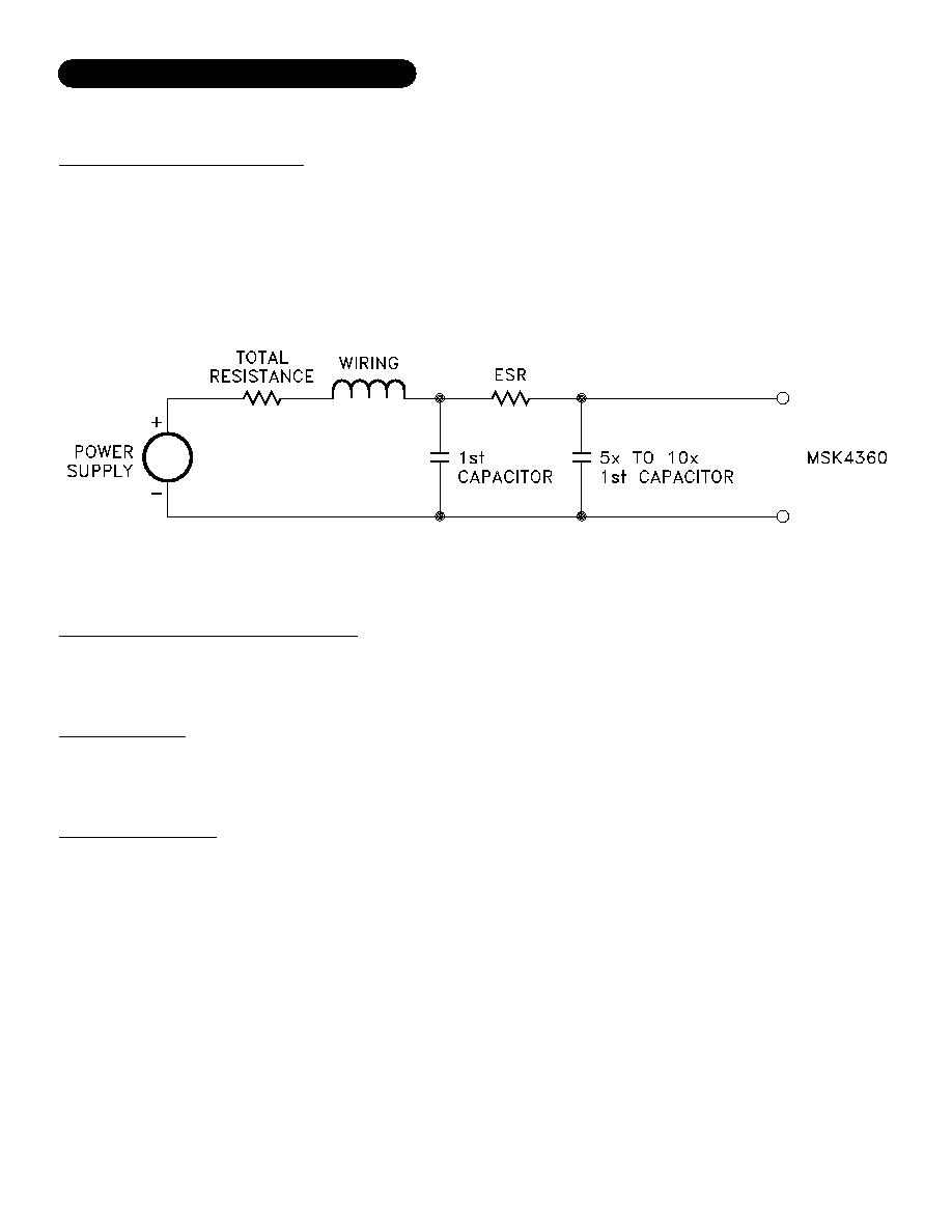
BUS VOLTAGE FILTER CAPACITORS
The size and placement of the capacitors for the DC bus has a direct bearing on the amount of noise filtered and also on the size
and duration of the voltage spikes seen by the bridge. What is being created is a series RLC tuned circuit with a resonant
frequency that is seen as a damped ringing every time one of the transistors switches. For the resistance, wire resistance, power
supply impedance and capacitor ESR all add up for the equivalent lumped resistance in the circuit. The inductance can be figured
at about 30 nH per inch from the power supply. Any voltage spikes are on top of the bus voltage and the back EMF from the
motor. All this must be taken into account when designing and laying out the system. If everything has been minimized, there is
another solution. A second capacitance between 5 and 10 times the first capacitor and it should either have some ESR or a
resistor can be added in series with the second capacitor to help damp the voltage spikes.
Be careful of the ripple current in all the capacitors. Excessive ripple current, beyond what the capacitors can handle, will destroy
the capacitors.
REGULATED VOLTAGE FILTER CAPACITORS
It is recommended that about 10 µF of capacitance (tantalum electrolytic) for bypassing the + and -15V regulated outputs be
placed as close to the module pins as practical. Adding ceramic bypass capacitors of about 0.1 µF to 1 µF will aid in suppressing
noise transients.
GENERAL LAYOUT
Good PC layout techniques are a must. Ground plane for the analog circuitry must be used and should be tied back to the SIG
GND. Ground plane for the power circuitry should be tied back to the V+ RTN pin, pin 16. Pin 16 should be connected to pin 10
external to the hybrid by a single thick trace. This will connect the two ground planes together.
LOW POWER STARTUP
When starting up a system utilizing the MSK 4360 for the first time, there are a few things to keep in mind. First, because of the
small size of the module, short circuiting the output phases either to ground or the DC bus will destroy the bridge. The current
limiting and control only works for current actually flowing through the bridge. The current sense resistor has to see the current
in order for the electronics to control it. If possible, for startup use a lower voltage and lower current power supply to test out
connections and the low current stability. With a limited current supply, even if the controller locks up, the dissipation will be
limited. By observing the E/A OUT pin which is the error amp output, much can be found out about the health and stability of the
system. An even waveform with some rounded triangle wave should be observed. As current goes up, the DC component of the
waveform should move up or down. At full current (with a regular supply) the waveform should not exceed +8 volts positive
peak, or -8 volts negative peak. Some audible noise will be heard which will be the commutation frequency. If the motor squeals,
there is instability and power should be removed immediately unless power dissipation isn't excessive due to limited supply
current. For compensation calculations, refer to the block diagram for all information to determine the amplifier gain for loop gain
calculations.
5
Rev. G 11/01
APPLICATION NOTES CONTINUED