5040data
The MSK 5046RH series are high efficiency, 4 amp, radiation hardened switching regulators. The output voltage is
configured for 1.5V, 2.5V, 3.3V or 5.0V internally with a tolerance of 1% at 1.5 amps. The operating frequency of
the MSK 5046RH is 400KHz. A low quiescent current and greater than TBD operating efficiency keep the total
internal power dissipation of the MSK 5046RH down to an absolute minimum. The device is packaged in a hermetic
power package for high reliability applications, and is available fully compliant to MIL-PRF-38534 Class H or K.
4707 Dey Road Liverpool, N.Y. 13088
M.S.KENNEDY CORP.
(315) 701-6751
FEATURES:
5046RH
SERIES
ISO-9001 CERTIFIED BY DSCC
RADIATION HARDENED
HIGH EFFICIENCY, 4 AMP
SWITCHING REGULATORS
Up To TBD% Efficiency For 5V Version
4 Amp Output Current
3.1V to 16V Input Range with Startup Bias
12V to 16V Input Range with UVLO (VBias=V
IN
)
Preset 1.5V, 2.5V, 3.3V or 5.0V Output Versions
Custom Output Voltages Available
400KHz Switching Frequency
Hermetic Package with Three Lead Form Options
-55°C to +125°C Operating Temperature Range
Total Dose Rated to TBDK RAD
DESCRIPTION:
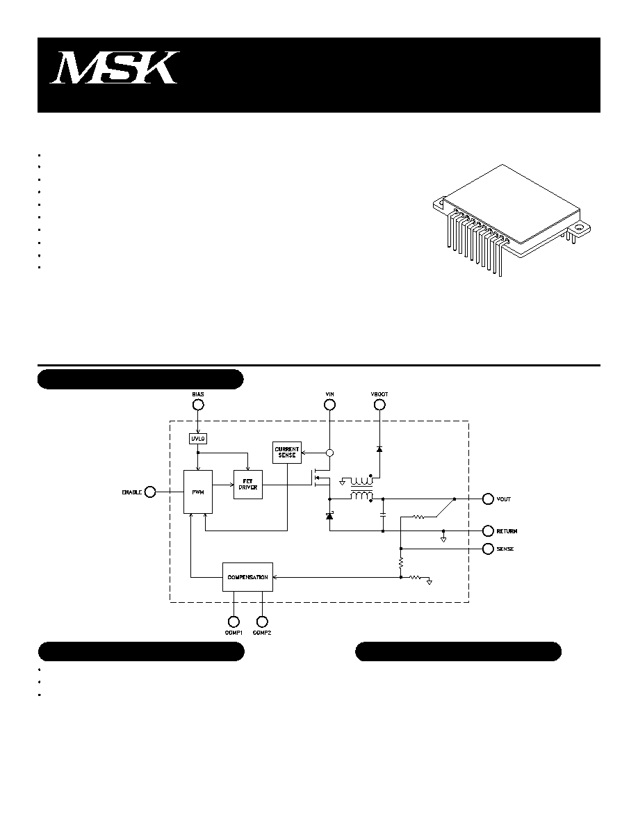
EQUIVALENT SCHEMATIC
MIL-PRF-38534 CERTIFIED
TYPICAL APPLICATIONS
PIN-OUT INFORMATION
Step-down Switching Regulator
Microprocessor, FPGA Power Source
High Efficiency Low Voltage
Subsystem Power Supply
TBD
TBD
TBD
TBD
TBD
TBD
TBD
TBD
TBD
TBD
1
2
3
4
5
6
7
8
9
10
20
19
18
17
16
15
14
13
12
11
TBD
TBD
TBD
TBD
TBD
TBD
TBD
TBD
TBD
TBD
PRELIMINARY Rev. A 6/03
1
T
ST
T
LD
T
C
T
J
Storage Temperature Range
Lead Temperature Range
(10 Seconds)
Case Operating Temperature
MSK5046RH Series
MSK5046RH K/H/E Series
Junction Temperature
ABSOLUTE MAXIMUM RATINGS
-65°C to +150°C
300°C
-40°C to +85°C
-55°C to +125°C
+150°C
Input Voltage
Enable
Output Current
Thermal Resistance (@ 125°C)
-0.3V, +16V
-0.3V, 10.5V
4.0 Amps
TBD°C/W
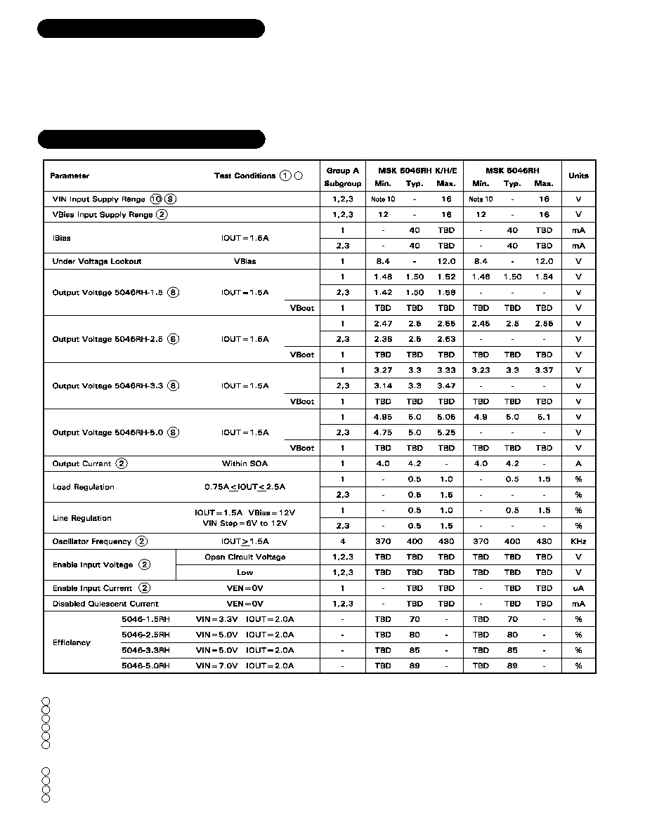
ELECTRICAL SPECIFICATIONS
PRELIMINARY Rev. A 6/03
2
NOTES:
1
2
3
4
5
6
8
9
10
11
V
IN
=12V, VBias=12V, I
OUT
=1.5A unless otherwise specified.
Guaranteed by design but not tested. Typical parameters are representative of actual device performance but are for reference only.
All output parameters are tested using a low duty cycle pulse to maintain T
J
= T
C
.
Industrial grade and 'E' suffix devices shall be tested to subgroup 1 unless otherwise specified.
Military grade devices ('H' and 'K' suffix) shall be 100% tested to subgroups 1,2 and 3.
Subgroup 1
Subgroup 2
Subgroup 3
Alternate output voltages are available. Please contact the factory.
The device can operate with input voltages as high as 16V, but efficiency is best at lower inputs.
With VBias connected to a separate source, V
IN
Min. is approximately 3.1V.
Contact factory for post radiation limits.
T
A
=T
C
=+25°C
T
A
=T
C
=+125°C
T
A
=T
C
=-55°C
11

APPLICATION NOTES
BOOTSTRAPPING:
The MSK 5046RH's Vboot output can be used to supply
bias voltage once the device is operating. Use a diode to "OR"
the startup bias supply with the Vboot output if the startup
supply voltage is less than Vboot. Use a switching scheme if
Vboot is less than or equal to Vstartup. Additional bypass
capacitance is required on the Vbias input pin when
bootstrapping the MSK 5046RH. The bootstrap voltage is
stepped up from the output voltage. Direct biasing of the Vbias
input may be more efficient due to the additional conversion
involved in bootstrapping.
PRELIMINARY Rev. A 6/03
3
INPUT CAPACITOR SELECTION:
The MSK 5046RH should have an external high frequency
ceramic capacitor (0.1uF) between VIN and GND. Connect a
low-ESR bulk capacitor directly to the input pin of the MSK
5046RH. Select the bulk input filter capacitor according to
input ripple-current requirements and voltage rating, rather than
capacitor value. Electrolytic capacitors that have low enough
ESR to meet the ripple-current requirement invariably have more
than adequate capacitance values. Aluminum-electrolytic ca-
pacitors are preferred over tantalum types, which could cause
power-up surge-current failure when connecting to robust AC
adapters or low-impedance batteries.
INPUT BIAS AND UVLO:
The Bias pin of the MSK 5046RH provides bias to the con-
trol circuitry. The Vbias pin can be connected directly to the
input bus for 12V to 16V operation or it can be biased sepa-
rately with a 12V to 16V source to extend the input range of
the device refer to the paragraph titled "INPUT VOLTAGE
RANGE". The MSK 5046RH's built in under voltage lockout
feature prevents damage to downstream devices in the event
of a drop in bias voltage. Under voltage lockout occurs at bias
voltages of approximately TBD rising and TBD falling. The
internal bias draws approximately 40mA under normal opera-
tion.
INPUT VOLTAGE RANGE
The MSK 5046RH's input range of 12V to 16V can be fur-
ther extended down to 3.1V by using a separate bias supply.
In this configuration very efficient low V to low V conversion
can be achieved.
The output capacitor values are generally determined
by the ESR and voltage rating requirements rather than
capacitance requirements for stability. Low ESR capaci-
tors that meet the ESR requirement usually have more
output capacitance than required for stability. Only spe-
cialized low-ESR capacitors intended for switching-regu-
lator applications, such as AVX TPS, Sprague 595D,
Sanyo OS-CON, Nichicon PL series or Kemet T510 se-
ries should be used.
The output ripple is usually dominated by the ESR of
the filter capacitors and can be approximated as IRIPPLE
x RESR. Including the capacitive term, the full equation
for ripple in the continuous mode is V
NOISE
(p-p)=I
RIPPLE
x (R
ESR
+ 1/(2
fC)).
OUTPUT CAPACITOR SELECTION:
SENSE:
ENABLE FUNCTION:
TBD
It is very important that the DC voltage returned to the
SENSE pin from the output be as noise and oscillation
free as possible. This voltage helps to determine the final
output and therefore must be a clean voltage. Excessive
noise or oscillation can cause the device to have an incor-
rect output voltage. Proper PC board layout techniques
can help to achieve a noise free voltage at the SENSE
pin.
COMPENSATION:
TBD

APPLICATION NOTES CONT'D
TYPICAL BOOTSTRAPPED APPLICATION
PRELIMINARY Rev. A 6/03
4

TYPICAL PERFORMANCE CURVES
PRELIMINARY Rev. A 6/03
5
TBD