4707 Dey Road Liverpool, N.Y. 13088
M.S.KENNEDY CORP.
(315) 701-6751
FEATURES:
SERIES
ISO-9001 CERTIFIED BY DSCC
Hermetic Surface Mount Package
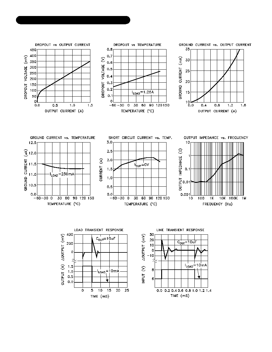
Extremely Low Dropout Voltage: 350mV @ 1.5 Amps
Available in 1.5V, 1.7V, 1.9V, 2.5V, 3.3V, 5.0V and 12.0V
On Board Thermal Shut Down
Reverse Battery and Load Dump Protection
Low Ground Current: 32mA Typical at Full Load
1% Maximum Guaranteed Accuracy
Output Current to 1.5 Amps
Alternate Output Voltages Available
DESCRIPTION:
The MSK 5215 series voltage regulators are available in +1.5V, +1.7V, +1.9V, +2.5V, +3.3V, +5.0V, and
+12.0V output configurations. All boast ultra low dropout specifications due to the utilization of a super PNP output
pass transistor with monolithic technology. Dropout voltages of 350mV at 1.5 amps are typical in this configuration,
which drives efficiency up and power dissipation down. Accuracy is guaranteed with a 1% maximum output voltage
tolerance. The MSK 5215 series is packaged in a space efficient 3 pin power surface mount ceramic package.
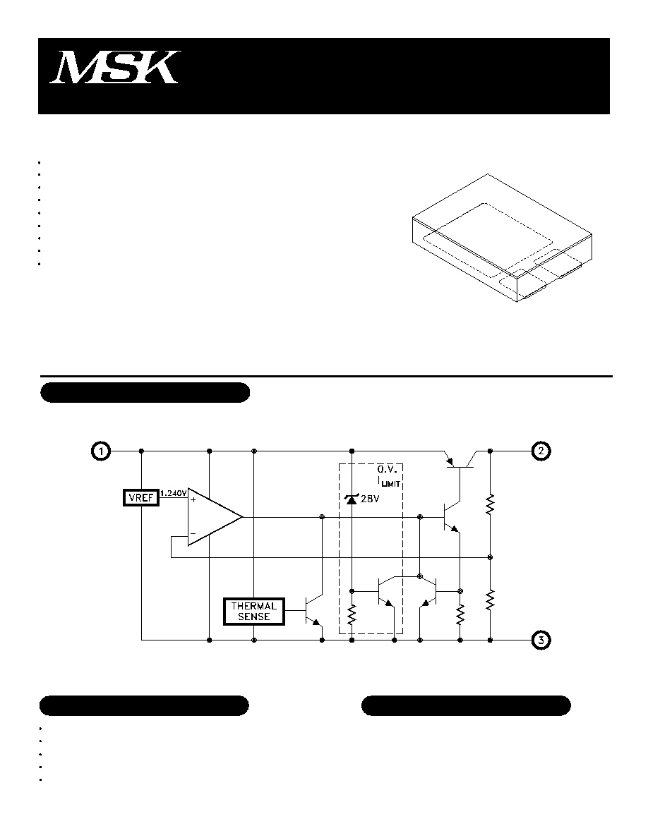
EQUIVALENT SCHEMATIC
5215
TYPICAL APPLICATIONS
PIN-OUT INFORMATION
High Efficiency, High Current Linear Regulators
Constant Voltage/Current Regulators
System Power Supplies
Switching Power Supply Post Regulators
Battery Powered Equipment
V
IN
V
OUT
Ground
1
2
3
1
Rev. E 11/04
MIL-PRF-38534 CERTIFIED
HIGH CURRENT, LOW DROPOUT
SURFACE MOUNT
VOLTAGE REGULATORS
Input Voltage (100mS 1%D.C.)
Input Voltage
Enable Voltage
Output Current
-20V to +60V
26V
-0.3V to 26V
3.5A
Storage Temperature Range . . -65°C to +150°C
Lead Temperature . . . . . . . . . . . . . . . . . 3 0 0 ° C
(10 Seconds Soldering)
Operating Temperature
MSK 5215 Series . . . . . . . . . . -40°C to +85°C
MSK 5215H/E Series . . . . . . . . -55°C to +125°C
V
INP
V
IN
V
EN
I
OUT
T
ST
T
LD
T
J
ABSOLUTE MAXIMUM RATINGS
2
Rev. E 11/04
Output Current Limit 2
Output Noise 2
Thermal Resistance 2
Thermal Shutdown 2
V
OUT
= -1%; I
OUT
= 100 mA
V
OUT
= -1%; I
OUT
= 1.5A
(V
OUT
+1V)
V
IN
26V
I
OUT
= 10 mA
V
OUT
= 0V; V
IN
= V
OUT
+1V
V
IN
= V
OUT
+1V; I
OUT
= 0.75A
V
IN
= V
OUT
+1V; I
OUT
= 1.5A
C
L
= 10µF; 10 H
Z
f
100 KH
Z
Junction to Case @ 125°C
T
J
Ground Current
2
1
2, 3
1
1
1
2, 3
1
2, 3
-
-
-
-
-
-
Parameter
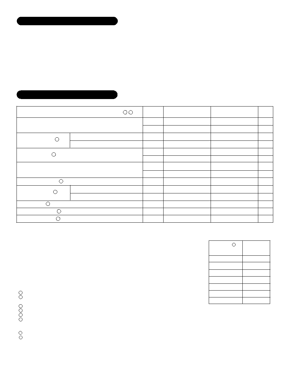
ELECTRICAL SPECIFICATIONS
-
-
-
-
-
-
-
-
-
-
-
-
-
-
±0.5
±1.0
80
350
±0.2
±0.3
±0.05
±0.5
2.1
18
32
400
3.5
130
±1.0
±2.0
200
600
±1.0
±2.0
±0.5
±1.0
3.5
30
-
-
4.0
-
%
%
mV
mV
%
%
%
%
A
mA
mA
µV
°C/W
°C
-
-
-
-
-
-
-
-
-
-
-
-
-
-
±0.5
-
80
350
±0.2
±0.3
±0.05
±0.5
2.1
18
32
400
3.5
130
±1.0
-
225
625
±1.2
-
±0.6
-
3.5
30
-
-
4.5
-
Group A
Subgroup
MSK 5215H/E SERIES
Min. Typ. Max.
MSK 5215 SERIES
Min. Typ. Max.
Units
Test Conditions
Output Voltage Tolerance
Dropout Voltage 2
Load Regulation 8
Line Regulation
I
OUT
= 10mA; V
IN
= V
OUT
+1V
MSK5215-1.5
MSK5215-1.7
MSK5215-1.9
MSK5215-2.5
MSK5215-3.3
MSK5215-5.0
MSK5215-12
+1.5V
+1.7V
+1.9V
+2.5V
+3.3V
+5.0V
+12.0V
OUTPUT
VOLTAGE
PART
NUMBER
1
2
3
4
5
6
7
8
NOTES:
Output decoupled to ground using 33µF minimum capacitor unless otherwise specified.
Guaranteed by design but no tested. Typical parameters are representative of actual
device performance but are for reference only.
All output parameters are tested using a low duty cycle pulse to maintain TJ = TC.
Industrial grade and "E" suffix devices shall be tested to subgroup 1 unless otherwise specified.
Military grade devices ('H' suffix) shall be 100% tested to subgroups 1,2,3.
Subgroup 1
Subgroup 2
Subgroup 3
Please consult the factory if alternate output voltages are required.
Due to current limit, maximum output current may not be available at all values of V
IN
-V
OUT
and temperatures.
See typical performance curves for clarification.
T
C
= +25°C
T
J
= +125°C
T
A
= -55°C
1 3
7
10 mA
I
OUT
1.25A
First, the power dissipation must be calculated as fol-
lows:
Power Dissipation = (Vin - Vout) x Iout
Next, the user must select a maximum junction tem-
perature. The absolute maximum allowable junction tem-
perature is 125°C. The equation may now be rearranged
to solve for the required heat sink to ambient thermal
resistance (R
sa).
EXAMPLE:
An MSK 5215-3.3 is configured for Vin=+5V and
Vout=+3.3V. Iout is a continuous 1A DC level. The
ambient temperature is +25°C. The maximum desired
junction temperature is 125°C.
R
jc = 3.5°C/W and R
cs = 0.5°C/W typically.
Power Dissipation = (5V - 3.3V) x (1A)
= 1.7 Watts
Solve for R
sa:
R
sa = 125°C - 25°C - 3.5°C/W - 0.5°C/W
In this example, a heat sink with a thermal resistance
of no more than 54°C/W must be used to maintain a
junction temperature of no more than 125°C.
APPLICATION NOTES
REGULATOR PROTECTION:
The MSK 5215 series is fully protected against re-
versed input polarity, overcurrent faults, overtemperature
conditions (Pd) and transient voltage spikes of up to 60V.
If the regulator is used in dual supply systems where the
load is returned to a negative supply, the output voltage
must be diode clamped to ground.
LOAD CONNECTIONS:
In voltage regulator applications where very large load
currents are present, the load connection is very impor-
tant. The path connecting the output of the regulator to
the load must be extremely low impedance to avoid af-
fecting the load regulation specifications. Any imped-
ance in this path will form a voltage divider with the load.
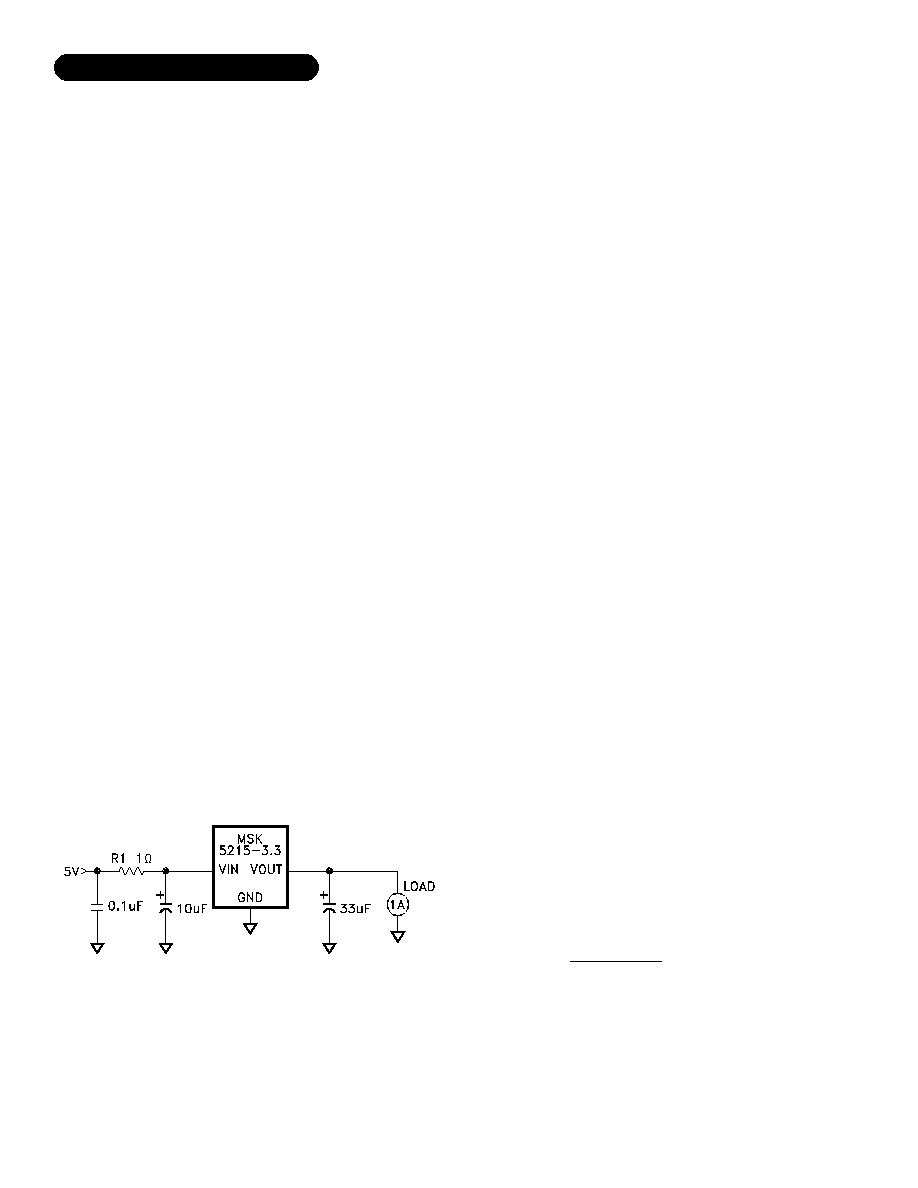
MINIMIZING POWER DISSIPATION:
Many applications can not take full advantage of the
extremely low dropout specifications of the regulator due
to large input to output voltage differences. The simple
circuit below illustrates a method to reduce the input
voltage at the regulator to just over the dropout specifi-
cation to keep the internal power dissipation minimized:
For a given continuous maximum load of 1 amp, R1
can be selected to drop the voltage seen at the regulator
to 4V. This allows for the output tolerance and dropout
specifications. Input voltage variations (5V) also should
be included in the calculations. The resistor should be
sized according to the power levels required for the ap-
plication.
OUTPUT CAPACITOR:
The output voltage ripple of the MSK 5215 series volt-
age regulators can be minimized by placing a filter ca-
pacitor from the output to ground. The optimum value
for this capacitor may vary from one application to the
next, but a minimum of 33µF is recommended for opti-
mum performance. Transient load response can also be
improved by placing a capacitor directly across the load.
The capacitor should not be an ultra-low ESR type. Tan-
talum capacitors are best for fast load transients but
aluminum electrolytics will work fine in most applica-
tions.
3
Rev. E 11/04
1.7W
PACKAGE CONNECTIONS:
The MSK 5215 series are highly thermally conductive
devices and the thermal path from the package heat sink
to the internal junctions is very short. Standard surface
mount soldering techniques should be used when mount-
ing the device. Some applications may require additional
heat sinking of the device.
HEAT SINK SELECTION:
To select a heat sink for the MSK 5215, the following
formula for convective heat flow may be used.
Governing Equation:
Tj = Pd x (R
jc + R
cs + R
sa) + Ta
WHERE:
Tj = Junction Temperature
Pd = Total Power Dissipation
R
jc = Junction to Case Thermal Resistance
R
cs = Case to Heat Sink Thermal Resistance
R
sa = Heat Sink to Ambient Thermal Resistance
Ta = Ambient Temperature
[
]
= 54.82°C/W
MSK5215-3.3 H
5
The information contained herein is believed to be accurate at the time of printing. MSK reserves the right to make
changes to its products or specifications without notice, however, and assumes no liability for the use of its products.
Please visit our website for the most recent revision of this datasheet.
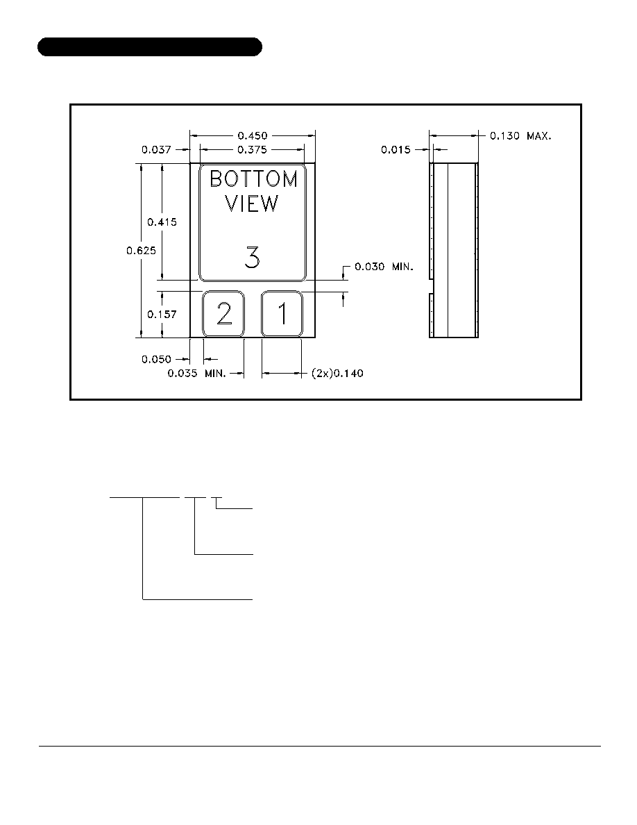
MECHANICAL SPECIFICATIONS
M.S. Kennedy Corp.
4707 Dey Road, Liverpool, New York 13088
Phone (315) 701-6751
FAX (315) 701-6752
www.mskennedy.com
ORDERING INFORMATION
SCREENING
BLANK=INDUSTRIAL; E=EXTENDED RELIABILITY
H=MIL-PRF-38534 CLASS H
OUTPUT VOLTAGE
1.5=+1.5V; 1.7=+1.7V; 1.9=+1.9V
2.5=+2.5V; 3.3=+3.3V; 5.0=+5.0V; 12=+12.0V
The above example is a +3.3V, Military regulator.
Rev. E 11/04
NOTE: ALL DIMENSIONS ARE ±0.010 INCHES UNLESS OTHERWISE LABELED.
GENERAL PART NUMBER