Äîêóìåíòàöèÿ è îïèñàíèÿ www.docs.chipfind.ru
TYPICAL APPLICATIONS
4707 Dey Road Liverpool, N.Y. 13088
(315) 701-6751
MIL-PRF-38534 CERTIFIED
5921RH
M.S.KENNEDY CORP.
FEATURES:
Satellite System Power Supplies
Switching Power Supply Post Regulators
Constant Voltage/Current Regulators
Microprocessor Power Supplies
RAD TOLERANT ULTRA LOW
DROPOUT ADJUSTABLE
POSITIVE LINEAR REGULATOR
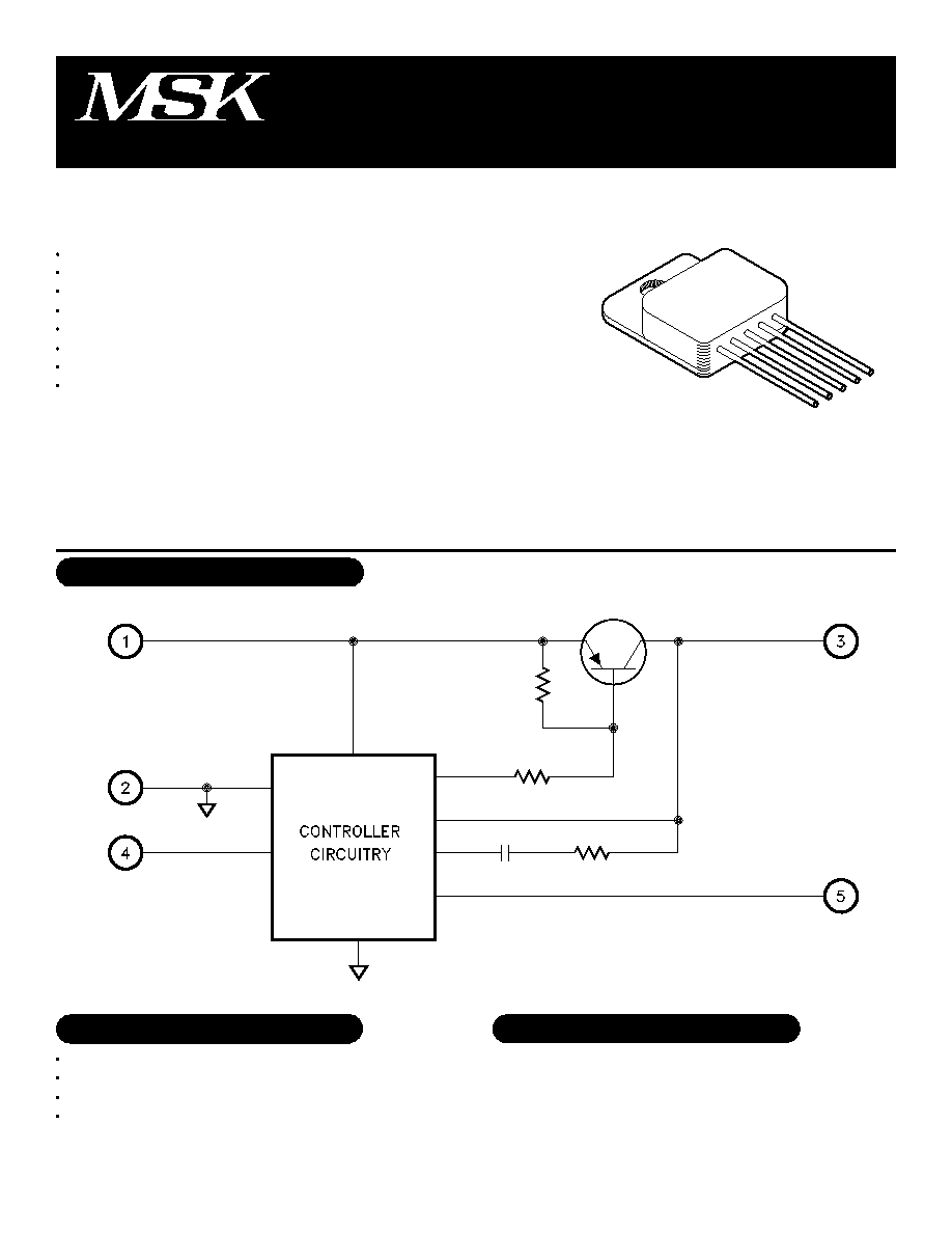
EQUIVALENT SCHEMATIC
TYPICAL APPLICATIONS
DESCRIPTION:
The MSK 5921RH is a rad tolerant adjustable linear regulator typically capable of delivering 5.0 amps of output
current. The typical dropout is only 0.30 volts with a 3.0A load. An external shutdown function is ideal for power
supply sequencing. This device also has latching overload protection that requires no external current sense resistor.
The MSK 5921RH is radiation tolerant and specifically designed for space/satellite applications. The device is pack-
aged in a hermetically sealed space efficient 5 pin SIP that is electrically isolated from the internal circuitry allowing for
direct heat sinking.
PIN-OUT INFORMATION
VIN
GND
VOUT
SHUTDOWN
ADJUST
Total Dose Tested to 300K RAD
Ultra Low Dropout for Reduced Power Consumption
External Shutdown
Latching Overload Protection
Adjustable Output Using Two External Resistors
Output Current Limit
Available in 3 Lead Form Options: Straight, Up and Down
Available to DSCC SMD # 5962-05220
1
2
3
4
5
Rev. C 1/06
1
Input Voltage Range
Feedback Voltage
Feedback Pin Current
Quiescent Current
Line Regulation
Load Regulation
Dropout Voltage
Minimum Output Current
Output Voltage Range
Output Current Limit
Shutdown Threshold
Ripple Rejection
Phase Margin
Gain Margin
Equivalent Noise Voltage
Thermal Resistance
Storage Temperature Range
Lead Temperature Range
(10 Seconds)
Power Dissipation
Junction Temperature
ABSOLUTE MAXIMUM RATINGS
+10V
5A
-55°C to +125°C
-40°C to +85°C
Supply Voltage
Output Current
Case Operating Temperature Range
MSK5921K/H/E RH
MSK5921RH
-65°C to +150°C
300°C
See SOA Curve
150°C
1
2
3
4
5
6
7
8
9
10
11
T
ST
T
LD
P
D
T
C
+V
IN
I
OUT
T
C
Unless otherwise specified, V
IN
=5.0V, R1=1.62K, V
SHUTDOWN
=0V and I
OUT
=10mA. See Figure 2.
Guaranteed by design but not tested. Typical parameters are representative of actual device performance but are for reference only.
Industrial grade and "E" suffix devices shall be tested to subgroups 1 and 4 unless otherwise requested.
Military grade devices ("H" suffix) shall be 100% tested to subgroups 1,2,3 and 4.
Subgroup 5 and 6 testing available upon request.
Subgroup 1,4 T
C
=+25°C
Subgroup 2,5 T
C
=+125°C
Subgroup 3,6 T
A
=-55°C
Output current limit is dependent upon the values of V
IN
and V
OUT
. See Figure 1 and typical performance curves.
Continuous operation at or above absolute maximum ratings may adversely effect the device performance and/or life cycle.
V
IN
shall be as specified or V
IN
Min, whichever is greater.
Not applicable when V
OUT
<V
IN
Min - dropout voltage maximum.
Consult factory for post radiation limits.
NOTES:
Group A
Subgroup
1
2,3
1
2,3
1,2,3
1
2,3
1
2,3
1
2,3
1
2,3
1
2,3
-
1
2,3
1
2,3
4
5,6
4,5,6
4,5,6
4,5,6
-
10mA
I
OUT
1.0A
I
OUT
=3.0A R1=187
V
FB
=1.265V 10mA
I
OUT
3.0A
V
IN
=6.5V
Not Including I
OUT
I
OUT
=50mA
V
OUT
+0.4V
V
IN
I
OUT
+1.3V
10mA
I
OUT
3.0A
Delta FB=1% I
OUT
=2.5A
2.8V
V
IN
6.5V
R1=187
V
IN
=6.5V
V
IN
=3.5V V
OUT
=2.5V
V
OUT
0.2V (OFF)
V
OUT
=Nominal (ON)
f=120Hz
I
OUT
=
50mA
Referred to Feedback Pin
Junction to Case @ 125°C Output Device
Typ.
-
-
1.265
-
-
14
14
±0.01
-
±0.06
-
0.22
0.26
8
9
-
4.0
4.0
1.3
1.3
-
-
70
18
-
2.2
Test Conditions
Max.
6.5
6.5
1.305
1.305
5.0
20
20
±0.50
±0.50
±0.80
±0.80
0.40
0.40
10
10
6.0
5.0
5.0
1.6
1.6
-
-
-
-
50
4.0
Min.
2.9
2.9
1.225
1.225
0
-
-
-
-
-
-
-
-
-
-
1.5
3.0
3.0
1.0
1.0
65
65
30
10
-
-
Min.
2.9
-
1.202
-
0
-
-
-
-
-
-
-
-
-
-
1.5
3.0
-
1.0
-
65
-
30
10
-
-
Max.
6.5
-
1.328
-
5.0
20
-
±0.60
-
±1.0
-
0.45
-
10
-
6.0
5.0
-
1.6
-
-
-
-
-
50
4.0
Typ.
-
-
1.265
-
-
14
-
0.01
-
0.06
-
0.22
-
8
-
-
4.0
-
1.3
-
-
-
70
18
-
2.2
V
V
V
V
µA
mA
mA
%V
OUT
%V
OUT
%V
OUT
%V
OUT
V
V
mA
mA
V
A
A
V
V
dB
dB
degrees
dB
µV
RMS
°C/W
MSK5921K/H/E
MSK5921
Parameter
ELECTRICAL SPECIFICATIONS
2
Units
1
2
2
2
7
2
2
2
2
2
2
8
7
10
9
9
11
Rev. C 1/06
APPLICATION NOTES
PIN FUNCTIONS
VIN - This pin provides power to all internal circuitry
including bias, start-up, thermal limit and overcurrent
latch. Input voltage range is 2.9V to 6.5V.
GND - Internally connected to ground, this pin should be
connected externally by the user to the circuit ground.
SHUTDOWN - There are two functions to the SHUT-
DOWN pin. It may be used to disable the output voltage
or to reset a current latch condition. To activate the shut-
down/reset functions the user must apply a voltage
greater than 1.6V to the SHUTDOWN pin. The output
voltage will turn on when the SHUTDOWN pin is pulled
below the threshold voltage. If the SHUTDOWN pin is
not used, it should be connected to ground. It should be
noted that with the shutdown pin tied to ground, a cur-
rent latch condition can only be reset by cycling power
off, then on.
VOUT - This is the output pin for the device.
ADJUST - The ADJUST pin is the inverting input of the
internal error amplifier. The non-inverting input is con-
nected to an internal 1.265V reference. This error ampli-
fier controls the drive to the output transistor to force
the ADJUST pin to 1.265V. An external resistor divider
is connected to the output, ADJUST pin and ground to
set the output voltage.
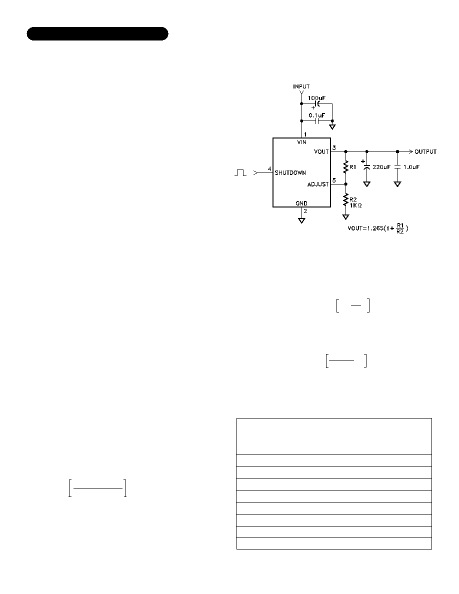
OUTPUT CAPACITOR SELECTION
Output capacitors are required to maintain regulation
and stability. A 220µF surface mount tantalum capacitor
in parallel with a 1.0µF ceramic capacitor from the out-
put to ground should suffice under most conditions. If
the user finds that tighter voltage regulation is needed
during output transients, more capacitance may be added.
If more capacitance is added to the output, the band-
width may suffer. ESR of the output capacitors should
be maintained at 0.1
to 1
.
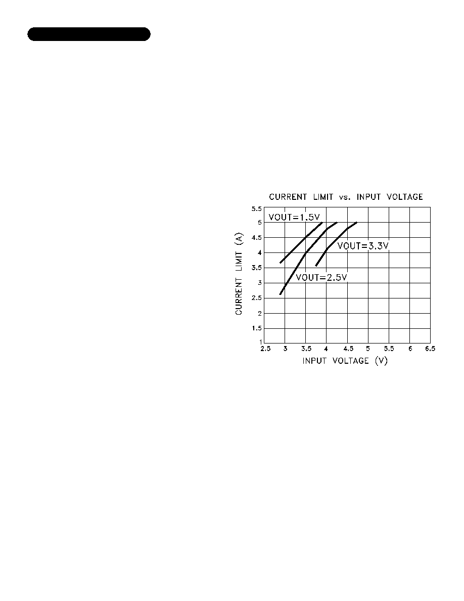
CURRENT LIMIT AND SOA
The MSK 5921RH current limit function is directly af-
fected by the input and output voltages. Figure 1 illus-
trates the relationship between VIN and ICL for various
output voltages. It is very important for the user to con-
sult the SOA curve when using input voltages which
result in current limit conditions beyond 4.5 Amps. When
using input voltages which result in current limit above
4.5 Amps, the user must maintain output current within
the SOA curve to avoid damage to the device. Note that
5 Amp maximum is due to current carrying capability of
the internal wirebonds.
3
OVERCURRENT LATCH
Overcurrent protection is provided by the MSK5921RH
series through the use of a timed latch off circuit. The
internal latch timeout is triggered by an overcurrent con-
dition. To allow for start up surge currents, the timeout
is approximately 5.5mS at 25°C. If the overcurrent con-
dition remains at the end of the timeout cycle, the regu-
lator will latch off until the latch is reset. The latch con-
dition can be reset by pulling the shutdown pin high or
cycling VIN off then back on. A thermal limit condition
will trigger the latch with no time out delay.
INPUT POWER SUPPLY BYPASSING
To maximize transient response and minimize power
supply transients it is recommended that a 100µF tanta-
lum capacitor is connected between VIN and ground. A
0.1µF ceramic capacitor should also be used for high
frequency bypassing.
FIGURE 1
Rev. C 1/06
APPLICATION NOTES CONT.
4
HEAT SINK SELECTION
To select a heat sink for the MSK 5921RH, the follow-
ing formula for convective heat flow may be used.
Governing Equation:
T
J
=
P
D
X (R
JC
+ R
CS
+ R
SA
) + T
A
Where
T
J
= Junction Temperature
P
D
= Total Power Dissipation
R
JC
= Junction to Case Thermal Resistance
R
CS
= Case to Heat Sink Thermal Resistance
R
SA
= Heat Sink to Ambient Thermal Resistance
T
A
= Ambient Temperature
Power Dissipation=(V
IN
-V
OUT
) x I
OUT
Next, the user must select a maximum junction tem-
perature. The absolute maximum allowable junction tem-
perature is 150°C. The equation may now be rearranged
to solve for the required heat sink to ambient thermal
resistance (R
SA
).
Example:
An MSK 5921RH is connected for V
IN
=+3.3V and
V
OUT
=+2.5V. I
OUT
is a continuous 3A DC level. The am-
bient temperature is +25°C. The maximum desired junc-
tion temperature is +125°C.
R
JC
=4.0°C/W and R
CS
=0.15°C/W for most thermal
greases
Power Dissipation=(3.3V-2.5V) x (3A)
=2.4Watts
Solve for R
SA:
125°C - 25°C
2.4W
= 36.5°C/W
In this example, a heat sink with a thermal resistance
of no more than 36.5°C/W must be used to maintain a
junction temperature of no more than 125°C.
TYPICAL APPLICATIONS CIRCUIT
OUTPUT VOLTAGE SELECTION
As noted in the above typical applications circuit, the
formula for output voltage selection is
A good starting point for this output voltage selection is
to set R2=1K. By rearranging the formula it is simple to
calculate the final R1 value.
Table 1 below lists some of the most probable resistor
combinations based on industry standard usage.
R1
R2
1+
V
OUT
=1.265
V
OUT
1.265
-1
R1=R2
1.5
1.8
2.0
2.5
2.8
3.3
4.0
5.0
R2
(
)
1K
1K
1K
1K
1K
1K
1K
1K
R1 (nearest 1%)
(
)
187
422
576
976
1.21K
1.62K
2.15K
2.94K
R
SA
= -4.0°C/W - 0.15°C/W
OUTPUT
VOLTAGE
(V)
THERMAL LIMITING
The MSK 5921RH control circuitry has a thermal shut-
down temperature of approximately 150°C. This ther-
mal shutdown can be used as a protection feature, but
for continuous operation, the junction temperature of the
pass transistor must be maintained below 150°C. Proper
heat sink selection is essential to maintain these condi-
tions.
TABLE 1
Rev. C 1/06
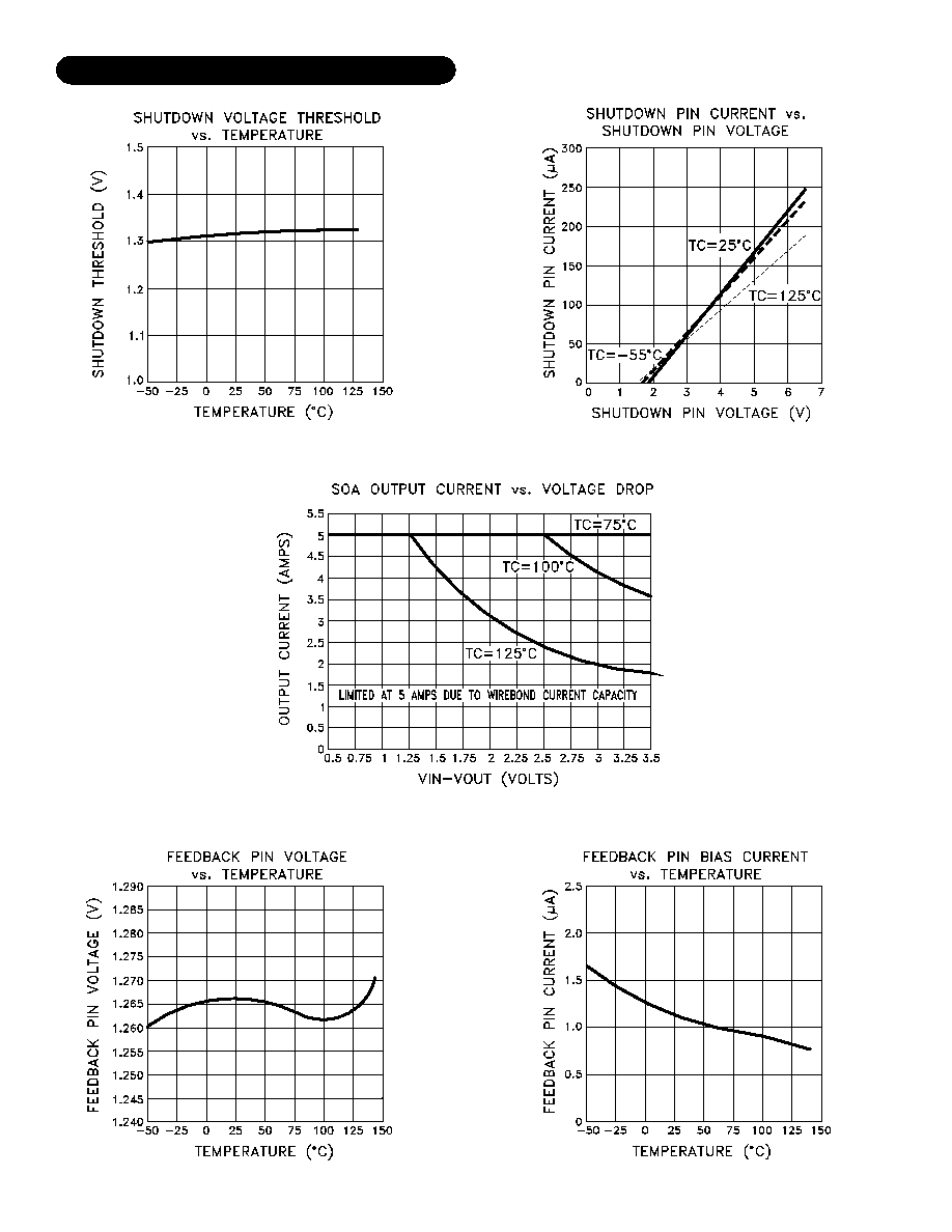
TYPICAL PERFORMANCE CURVES
5
Rev. C 1/06