
DESCRIPTION
The QCH28515T/RCH28515T series of DC-DC convert-
ers provides the ruggedness, reliability and features re-
quired to meet the advanced challenges of today's hi-rel
market. This family of converters uses all surface-mounted
hybrid components including magnetics, all ceramic capaci-
tors and ultrasonic wirebonds to give long life in full tempera-
ture range and high acceleration environments. There is no
power derating anywhere in the ≠55įC to 125įC operating
range.
This product family is tolerant of many types of faults
including load short, load overload, loss of voltage feedback,
large forward and reverse voltages applied to the synchroniza-
tion pin and input overvoltage. This converter family will
operate during input transients to 80 volts. The output voltages
have little overshoot during the input voltage transient such
that typical logic and linear parts on the outputs will stay well
within data sheet absolute maximums.
Other operational features include low duty factor current
limit and dynamic current limit threshold. The current limit
operates in a cyclic on-off mode with an on time of about 2
milliseconds and an off time of 20 milliseconds for a duty factor
of about 10 percent. This limits the converter dissipation to
about 1 watt, so there is no danger of overheating during an
output fault at 125į C. The dynamic current limit threshold
allows over 50 percent more current to flow for a short time
after power application, release from shutdown or recovery
from previous current limit allowing large load capacitances to
be charged during turn-on.
This converter family is a push-pull 400 kHz forward con-
verter with full isolation between the input side, output side and
case. This isolation is achieved without optocouplers for an
even greater margin of reliability. The converter is housed in
a power DIP package and is hermetically sealed. The
RCH28515T has tabs for bolting the device down.
EXTERNAL CONNECTIONS
BLOCK DIAGRAM
HI-REL DESIGN
REPLACES APEX DT28515T/F
WAVE SOLDERABLE PACKAGE
ALL CERAMIC CAPACITORS
NO OPTOCOUPLERS
SURFACE MOUNT MAGNETICS
WITHSTANDS 3000 G Y1 AXIS
OVER-VOLTAGE PROTECTION (OVP) OPTION
OTHER FEATURES TRIPLE OUTPUT
NO DERATING 55įC TO +125įC
WIDE SUPPLY RANGE 16 TO 40 VOLTS
HIGH ISOLATION 500V
HIGH POWER DENSITY 23 W/in
3
REMOTE SHUTDOWN
EXTERNAL SYNCH INPUT (FULLY TTL COMPATIBLE
OPTION)
1
10
2
9
3
8
4
7
5
6
POSITIVE
INPUT
+5 OUT
OUT COMMON
≠15 OUT
+15 OUT
INPUT
COMMON
SYNCH
INHIBIT
CASE GND
CASE GND
TOP VIEW
INPUT
MAGNETICS
AND
FILTER
PUSH≠PULL
PWM
PRIMARY
SIDE
FAILSAFES
OUTPUT
MAGNETICS
AND
FILTER
POWER
MAGNETICS
FEED≠BACK
MAGNETICS
SECONDARY
SIDE
FAILSAFES
Ī
15 V
LINEAR
REGS
V
in
+Aux
≠Aux
MAIN
OUTPUT
4707 Dey Road Liverpool, N.Y. 13088
M.S.KENNEDY CORP.
(315) 701-6751
QCH28515T/
RCH28515T
ISO-9001 CERTIFIED BY DSCC
30W TRIPLE
DC-DC
CONVERTERS
PRELIMINARY Rev. - 5/01
1
QCH28515T
RCH28515T

SPECIFICATIONS
INPUT VOLTAGE
V
IN
No load
1, 2, 3
0
28
50
Vdc
Normal
to full load
16
40
Operating
1
50
80
Vpk
Transient
UVLO
V
UVLO
1, 2, 3
10
12.5
14
Vdc
INPUT CURRENT
I
IN
NoLoad
1, 2, 3
0.12
Adc
Full load
2
1.25
1.57
1.65
Inhibited
0.0001
0.002
0.005
OUTPUT CURRENT
3
I
MAIN
1
4.00
6.00
Adc
2, 3
I
+AUX
1
0.33
0.66
2, 3
I
-AUX
1
-0.33
-0.66
2,3
OUTPUT VOLTAGE
2,4
V
MAIN
1
4.95
5.0
5.05
Vdc
2,3
V
+AUX
1
14.85
15.00
15.15
2, 3
V
-AUX
1
-14.85
-15.00
-15.15
2, 3
OVP
4
V
OVP
1
5.3
5.6
5.9
Vdc
2, 3
5.14
6.10
OUTPUT POWER
P
OUT
P
MAIN
1, 2, 3
0
20
30
W
PĪ
AUX
0
10
20
P
TOT
0
30
P
OVERLOAD
30
35
65
(5)
EFFICIENCY
2
1
63
%
2, 3
LINE REGULATION
VR
LINE
V
IN
1
5
10
mV
Main
16-40V
2, 3
10
50
1
50
75
Aux
2, 3
120
150
LOAD REGULATION
VR
LOAD
I
MAIN
1
5
20
mV
Main
0
4A
2, 3
20
50
ĪI
AUX
1
50
75
Aux
0
0.33A
2, 3
150
250
INPUT VOLTAGE RANGE
0 to 50 VDC
INPUT VOLTAGE TRANSIENT RANGE
80V@50mS
OUTPUT WITHSTAND VOLTAGE
25 VDC
STORAGE TEMPERATURE
≠65 to +150įC
OPERATING TEMPERATURE
≠55 to +125įC
TEMPERATURE, pin soldering 10 seconds
300 įC MAX
ABSOLUTE MAXIMUM RATINGS
ABSOLUTE MAXIMUM RATINGS
SPECIFICATIONS
QCH28515T/RCH28515T
TEST
GROUP A
12
PARAMETER
SYMBOL
CONDITIONS
SUBGROUP MIN TYPICAL
MAX
UNITS
COMMENT
Unless noted: ≠55įC
T
CASE
125įC, 16Vdc
V
IN
40Vdc, P
MAIN
= 20W, P+
AUX
= P-
AUX
= 5W.
2
PRELIMINARY Rev. - 5/01

CROSS REGULATION
VR
CROSS
ĪI
AUX
1
5
20
mV
Main
0
0.33A
2, 3
20
50
I
MAIN
1
50
75
ĪAux
0
4A
2, 3
150
250
CURRENT LIMIT
I
LIM
1
115
125
%
2, 3
LOAD FAULT POWER
P
D
Overload
6
1, 2, 3
14
25
W
Short Ckt.
6
INHIBIT PIN VOLTAGE
7
V
ENH
Enabled
1, 2, 3
12
16.8
V dc
V
ENL
Inhibited
0
5
INHIBIT PIN CURRENT
7
I
ENH
Enabled
1, 2, 3
0
10
ĶA dc
I
ENL
Inhibited
650
1200
1800
ISOLATION
R
ISO
500V dc
1, 2, 3
100
Meg
Primary
to Secondary to Case
CAPACITIVE LOAD
C
L
1, 2, 3
330
500
ĶF
Main
10
22
ĪAux
INPUT CURRENT RIPPLE
2
I
RIP
1
100
mA rms
2, 3
120
250
OUTPUT VOLTAGE RIPPLE
V
RIP
1
15
45
mV rms
Main
2, 3
30
90
1
12
36
ĪAux
2 ,3
25
75
SWITCHING FREQUENCY
F
SW
4, 5, 6
350
400
450
kHz
SYNC. FREQUENCY
F
SYNC
4, 5, 6
300
650
kHz
SYNC. PIN VOLTAGE
8
V
HI
1, 2, 3
2.4
≠
V dc
V
LO
≠
0.4
SYNC. PIN CURRENT
I
SYN
H
1, 2, 3
-400
ĶA dc
I
SYN
L
-500
-750
TURN ON TIME
9
T
ON
4
4
8
mS
TURN ON OVERSHOOT
VT
ON
C
L
=0
4
0
300
mVdc
Main
4
900
ĪAux
STEP LOAD TRANSIENT,
VT
LOAD
C
L
=0, I
MAIN
=50
100%
1
-800
+800
mVdc
Main
RESPONSE
C
L
=0, I
AUX
=50
100%
1
500
750
ĪAux
SPECIFICATIONS
QCH28515T/RCH28515T
TEST
GROUP A
12
PARAMETER
SYMBOL
CONDITIONS
SUBGROUP MIN TYPICAL
MAX
UNITS
COMMENT
Unless noted: ≠55įC
T
CASE
125įC, 16Vdc
V
IN
40Vdc, P
MAIN
= 20W, P+
AUX
= P-
AUX
= 5W.
3
PRELIMINARY Rev. - 5/01

STEP LOAD TRANSIENT
10
TR
LOAD
C
L
=0
4
0.05
0.10
mS
Main
RECOVERY
4
3 5
ĪAux
STEP LINE TRANSIENT,
VT
LINE
C
L
=0
1
150
250
mVdc
Main
RESPONSE
1
100
250
ĪAux
STEP LINE TRANSIENT
10
TR
LINE
C
L
=0
4
0.05
0.10
mS
Main
RECOVERY
4
3
5
ĪAux
LOAD FAULT TRANSIENT,
VT
FLT
C
L
=0
1
0
300
mVdc
Main
RESPONSE
1
900
ĪAux
LOAD FAULT TRANSIENT
10
, TR
FLT
C
L
=0
4
40
100
mS
Main
RESPONSE
4
TBD
ĪAux
INHIBIT DELAY
11
TD
INH
C
L
=0
4
0.1
0.2
mS
Main
4
TBD
ĪAux
INHIBIT RECOVERY
9
TR
INH
C
L
=0
4
4
8
mS
Main
4
TBD
ĪAux
SPECIFICATIONS
QCH28515T/RCH28515T
NOTES: 1.
Under Voltage Lock Out (UVLO) is approx. 10.5-13.5 Vdc.
2.
Vin = 28Ī1 V dc. Nominal output power: P
MAIN
= 20W, P+
AUX
= 5W, P-
AUX
= 5W.
3.
Full power output must be equal to or less than 30 watts. Short duration Aux current is 2A peak.
4.
Over-Voltage Protection (OVP) guaranteed by design not to exceed 6V dc on main output under any static condition at room
temperature. On models with OVP option, only. Therefore this parameter is limited to <5.5V on these models.
5.
Short Term Over-Load (STOL).
6.
Continuous overload. Auxiliary outputs are protected with thermal shutdown.
7.
Internal Pull-Up typically 22k ohms to V
IN
. For 80-volt transients, input device must be able to sink at least 3.5 mA.
8.
Internal Pull-Up approximately 22k ohms to typically 12V. This is an open collector, TTL compatible, edge triggered active low
input. A valid low must exist for 20% to 80% duty ratio. The converter takes approximately 2 mS to synchronize. For "TTL
Sync" option V
MAX
55V.
9.
Time for outputs to reach 90% of final value. Measured from valid Inhibit High V
ENH
or valid V
IN
.
10.
Measured from start of transient to response within 90% of final value.
11.
Time for outputs to reach 50% of initial value. Measured from valid Inhibit Low V
ENL
or V
IN
below UVLO.
12.
As per MIL-PRF-38534.
TEST
GROUP A
12
PARAMETER
SYMBOL
CONDITIONS
SUBGROUP MIN TYPICAL
MAX
UNITS
COMMENT
Unless noted: ≠55įC
T
CASE
125įC, 16Vdc
V
IN
40Vdc, P
MAIN
= 20W, P+
AUX
= P-
AUX
= 5W.
4
PRELIMINARY Rev. - 5/01
QCH28515T/RCH28515T
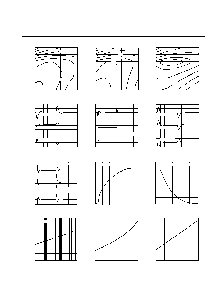
TYPICAL PERFORMANCE GRAPHS
0
0
20
40
60
80
100
.5
1
1.5
2
2.5
3.0
TIME, t (200
Ķ
sec/DIV)
0
1
2
3
4
5
6
LOAD TRANSIENT RESPONSE
OUTPUT RESPONSE
100K
≠50
0
20
40
60
80
100
0
50
100 125
1K
100
10K
INPUT VOLTAGE, V
IN
(V)
TIME, t (1 mS/DIV)
LINE TRANSIENT RESPONSE
STARTUP
SHUTDOWN
EFFICIENCY CONTOURS
16
28
40
32
36
20
24
PERCENT OUTPUT LOAD
90
50
70
60
80
100
FREQUENCY, F
TEMPERATURE (
į
C)
≠80
≠70
≠50
≠60
≠40
≠30
≠20
AUDIO REJECTION
REJECTION, DB
INPUT VOLTAGE MINIMUM
PERCENT LOAD
16
15
14
13
12
INPUT VOLTAGE MINIMUM
INPUT VOLTAGE, (V)
14
13.5
13
12.5
12
INPUT VOLTAGE, (V)
V
IN
= 4V P-P
V
IN
= 16, 50V
Tr , Tf = 10
Ķ
S
V
IN
= 16, 50V
Tr , Tf = 10
Ķ
S
TEMP = 25
į
C
TEMP = 125
į
C
67%
68%
69%
70%
72.5%
70%
71%
72%
INPUT VOLTAGE, V
IN
(V)
EFFICIENCY CONTOURS
16
28
40
32
36
20
24
PERCENT OUTPUT LOAD
90
50
60
70
80
100
61%
62%
63%
60%
64.5%
64%
63%
62%
61%
INPUT VOLTAGE, V
IN
(V)
EFFICIENCY CONTOURS
15
30
40
35
35
20
25
PERCENT OUTPUT LOAD
80
90
50
60
70
100
TEMP =
≠55
į
C
66%
67%
68%
72%
69%
69%
70%
71%
TIME, t (200
Ķ
sec/DIV)
TIME, mS
TIME,
Ķ
S
LINE TRANSIENT RESPONSE
OUTPUT RESPONSE, 5V
0
1
2
3
4
5
6
OUTPUT RESPONSE, 5V
TIME, t (1 mS/DIV)
LOAD TRANSIENT RESPONSE
TOTAL CONVERTER LOAD 15W
TOTAL CONVERTER LOAD 15W
≠15V
15V
5
V
OUTPUT RESPONSE
≠15V
15V
5V
OUTPUT RESPONSE
≠15V
15V
5
V
OUTPUT RESPONSE
≠15V
15V
5
V
C
L
= 100
Ķ
F, 22
Ķ
F, 22
Ķ
F
C
L
= 100
Ķ
F, 22
Ķ
F, 22
Ķ
F
500 mV/DIV
200 mV/DIV
20 mV/DIV
20 mV/DIV
TOTAL CONVERTER LOAD 30W
500 mV/DIV
500 mV/DIV
20 mV/DIV
20 mV/DIV
50 mV/DIV
I
LOAD
(5V) = 2A, 4A
I
LOAD
(5V) = 2A, 4A
50 mV/DIV
50 mV/DIV
50 mV/DIV
5
PRELIMINARY Rev. - 5/01
SYNCHRONIZATION
The synch pin allows the converter to be synchronized in
frequency and phase with an external signal. This signal
should be TTL compatable (0.8 max V
INL
and 2.0 V min V
INH
).
Overdrive up to 10V is not harmful. Transient voltage withstand
is Ī 50V with respect to input common. The frequency applied
to this pin must be between 350 and 600 kHz with duty factor
anywhere from 20 to 80 percent.
SHUTDOWN
The shutdown pin turns off the power conversion circuits and
puts the converter in standby mode. The shutdown pin is
referenced to the input common pin. In standby mode the
converter only draws 2.2 mA typical (5.0 mA maximum) input
current from V
IN
. For normal operation this pin should be open
circuited and allowed to float. For shutdown pull this pin below
1 volt. The maximum open circuit voltage that will appear on
this pin is 15 volts. See graphs for typical time response of the
converter to assert and release shutdown.
QCH28515T/RCH28515T
APPLICATION INFORMATION
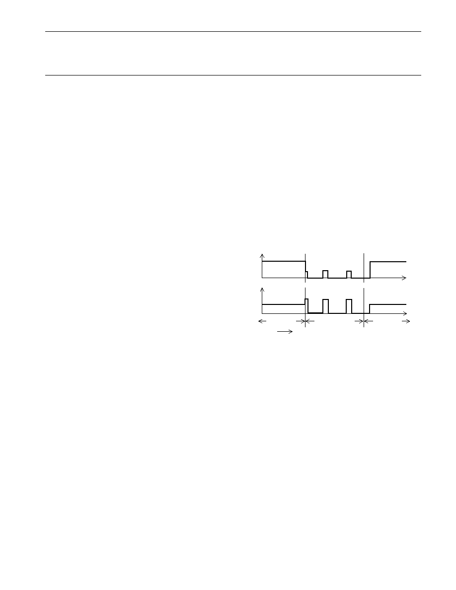
LOAD FAULT RESPONSE
The QCH28515T/RCH28515T family of DC-DC convert-
ers use a common fault protection approach. Load fault
conditions include short-circuit and overload conditions. The
QCH28515T/RCH28515T converters respond to load faults
on the main output (+5V) by turning off all power conversion
circuits for a period of time and then attempting to restart. The
figure below shows the fault protection response to an output
overload, the turn on plus detect fault time is typically two
milliseconds and the off time is typically twenty milliseconds.
The net "on" duty factor during a fault is only 10 percent,
resulting in low converter dissipation and immunity from
overheating at 125įC. An added benefit to this method is that
the amount of output current that defines a fault is pro-
grammed to increase by 1.5X during the first few hundred
microseconds of operation after power-up, load fault recov-
ery or release of the shutdown pin. This allows QCH28515T/
RCH28515T converters to bring up capacitive and other
difficult loads more reliably than some competing converters.
NORMAL
TIME
NORMAL
LOAD FAULT
Vo
I
o
The auxiliary outputs have individual overcurrent protection
and independent fault protection. A rapid response thermal
shutdown feature adds to the reliability of the converter by
protecting each auxiliary output from load faults. Substantial
current may drawn from either auxiliary output but is limited to
safe levels by independent current sensing circuitry on each.
If the fault or overload continues for extended periods the
thermal shut down circuitry will cycle the output to limit the
maximum internal hotspot temperature to a safe level.
6
PRELIMINARY Rev. - 5/01
The information contained herein is believed to be accurate at the time of printing. MSK reserves the right to make
changes to its products or specifications without notice, however, and assumes no liability for the use of its products.
Please visit our website for the most recent revision of this datasheet.
M.S. Kennedy Corp.
4707 Dey Road, Liverpool, New York 13088
Phone (315) 701-6751
FAX (315) 701-6752
www.mskennedy.com
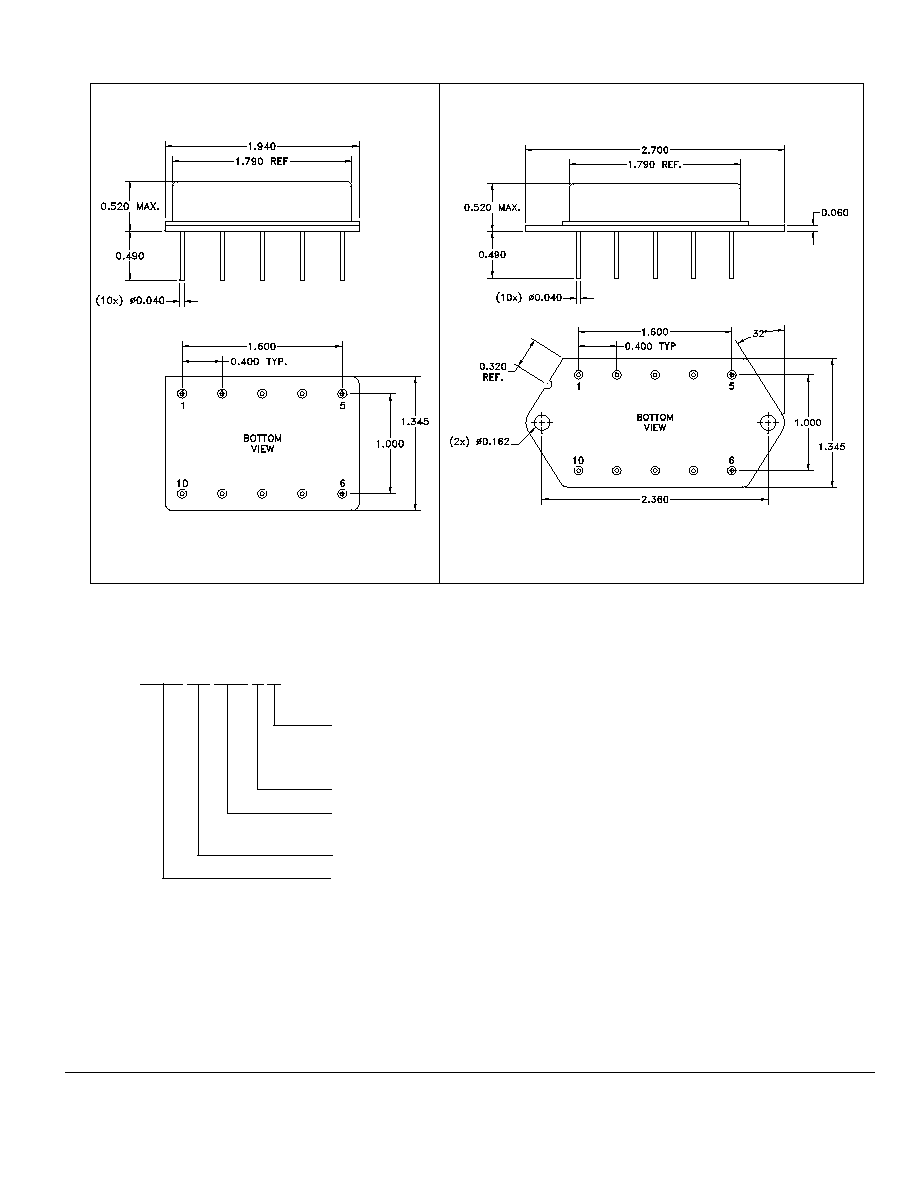
NOTE: ALL DIMENSIONS ARE Ī0.010 INCHES UNLESS OTHERWISE LABELED.
ESD Triangle indicates Pin 1.
QCH28515T
The above example is an industrial grade 5V and Ī15V triple output converter
without tabs
ORDERING INFORMATION
SCREENING
BLANK= INDUSTRIAL; E= EXTENDED RELIABILITY;
H= CLASS H; K= CLASS K
TRIPLE OUTPUT
OUTPUT VOLTAGES
515=5V AND Ī15V
NOMINAL INPUT VOLTAGE
GENERAL PART NUMBER (QCH=NO TABS; RCH=TABS)
7
MECHANICAL SPECIFICATIONS
PRELIMINARY Rev. - 5/01
QCH28515T
RCH28515T