!
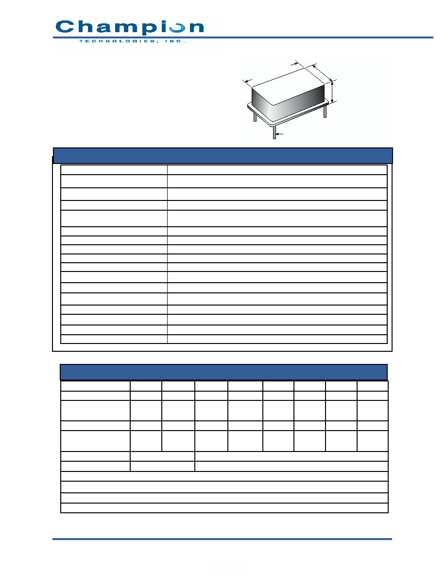
4-pin Package, Compatible with 14-pin DIL
!
40 to 160MHz Frequency Range (Discrete Higher
Frequencies Available
!
Designed to Drive Standard ECL 10K and 10KH
Families
!
ECL and PECL Options Available
!
Dual Complementary Output Available
!
50
Drive Capability
!
Internal 470W Output Pull-Down Resistor Available
2553 N. Edgington Street, Franklin Park, IL 60131 " Phone: 847.451.1000 " Fax: 847.451.7585
800-888-1499 or www.champtech.com
1
MODEL
See Part Numbering Guide Below
Frequency Range (MHz)
40 to 160
Frequency Stability (ppm)
Overall
Inclusive of calibration, temperature, voltage, load, shock,vibration, aging
0�C to 70�C
�100
Temperature Range (�C)
Operating
0�C to +70�C
Storage
-55�C to +125�C
Supply Voltage (V)
Supply Current (mA)
ELECTRICAL SPECIFICATIONS
Start up Time (ms)
<10
K1149 Series
5V Crystal Clock Oscillators
K1149
100.000
MHZ
CTI DA
TE CODE
6,22*
mm
Max.
20,8 mm Max.
13,2 mm Max.
PIN 1
Typical
28; 55 on R-Suffix (Option 3)
Jitter (Typical)
5ps RMS @ 40MHz
PIN
K1149AB
K1149AC
K1149AM
PART NUMBERING GUIDE (Use this chart for ordering)
1
7
8
14
Case GND
N/C
N/C
VSS
VEE
ECL Out
VEE
ECL Out
VSS &
Case GND
ECL Out
VEE
Maximum
60; 90 on R-Suffix (Option 3)
Frequency (MHz)
Option
40 to 160
2, 3
VSS &
Case GND
K1149AA
Case GND
VEE
ECL Out
VSS
K1149BA K1149BC K1149BM K1149CA
Higher Frequency Available (MHz)
180, 200, 220
-5.2 � 5%
+5.0 � 5%
ECL (VEE)
PECL (VCC)
Comp. Out
VSS &
Case GND
PECL Out
VCC
Comp Out
VEE
ECL Out
VSS &
Case GND
Comp Out
VSS &
Case GND
ECL Out
VEE
N/C
VEE &
Case GND
PECL Out
VCC
40 to 125
1, 2, 3
Options Available
1. Optional +5.0 � 10% Operation at VSS
2. 50ppm (K1149XX5 available only in frequency range of 40MHz to 160MHz
3. Optional internal pull down resistor available only in the range of 40MHz to 160MHz - K1149XX-R
*> 140MHz (Height) = 8,51mm Max
2553 N. Edgington Street, Franklin Park, IL 60131 " Phone: 847.451.1000 " Fax: 847.451.7585
800-888-1499 or www.champtech.com
2
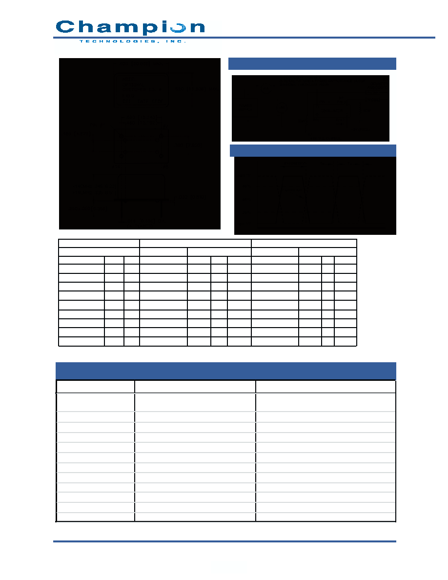
OUTPUT WAVEFORM
TEST CIRCUIT DIAGRAM
K1149 Series
5V Crystal Clock Oscillators
TEST METHODS
REFERENCE PROCEDURES
DESCRIPTION
Temperature Cycle
MIL-STD-833, Mtd 1010, Cond. B
Mechanical Shock
MIL-STD-883, Mtd 2002, Cond. B
-55�C to +125�C; Air-to-Air; 100 cycles; 10
min. dwell
Vibration
MIL-STD 883, Mtd 2007, Cond. B
20-2000 Hz; 0.06 inch; 15g's; 3 planes
Humidity Steady State
MIL-STD-202, Mtd 103
40�C; 90%-95% R.H.; 56 days
Thermal Shock
MIL-STD-883, Mtd 1011.7 Cond. B
Electrostatic Discharge
Solderability
Hermeticity
Resistance to Soldering
Lead Integrity
Marking Permanence
Life Test
100�C to 0�C; Water-to-Water; 15 cycles
2 KV to 4 KV Threshold
Solder dip; Meniscograph Criteria
Mass spectro. 2 x 10⁻⁸ atmos. CC/sec He
235�C; 30 seconds
Lead tension & bend stress
Resistance to solvents
1500 g's
MIL-STD-883, Mtd 3015 Class II
MIL-STD-883, Mtd 1005.6
MIL-STD-883, Mtd 2022.2
MIL-STD-883, Mtd 1014.8, Cond. A1
MIL-STD-202, Mtd 210D, Cond. J
MIL-STD-883, Mtd 2004.5, Cond. A, B1
MIL-STD-883, Mtd 2015.8
125
�C, powered, 1000 hours minimum
MECHANICAL AND ENVIRONMENTAL SPECIFICATIONS
Parameter
Symbol Units
Test Condition
Min.
Typ.
Max.
Ground Reference
Power Supply (PECL)
"0" Level
"1" Level
Rise Time
Fall Time
Overlap
Symmetry
VSS
VCC
VOL
VOH
TR
TF
TOL
S
Volts
Volts
Volts
Volts
ps
ps
ps
%
Reference
Reference
50
into VCC-2
50
into VCC-2
50
into, 20% to 80%
50
into, 80% to 20%
50%
VCC -1.3
0
4.75
5.0
5.25
VCC-1.95
VCC-1.6
VCC-1.02
VCC-1.74
2.0
2.0
1.0
40
60
1.0
Test Condition
Reference
N/A
50
into VSS-2
50
into VSS-2
50
into, 20% to 80%
50
into, 20% to 80%
Power Supply (ECL)
VEE
Volts Reference
50%
VSS -1.3
PECL
Specifications
ECL
Min.
Typ.
Max
1.0
0
-5.2
-
N/A
VSS-1.95
VSS-1.6
VSS-1.02
VSS-0.74
1.0
2.0
1.0
2.0
1.0
40
60
Specifications