Document Outline
- Application Benefits
- Distinctive Characteristics
- General Description
- Operational Overview
- Pin Descriptions
- MII Interface
- RXD[3:0] (Receive Data, Input, TTL)
- RX_DV (Receive Data Valid, Input, TTL)
- RX_ER (Receive Error, Input, TTL)
- RX_CLK (Receive Clock, Input, TTL)
- CRS (Carrier Sense, Input, TTL)
- COL (Collision, Input, TTL)
- Tag Port Interface
- Result Port Interface
- Control Interfaces
- Host Processor Interface
- /PCS (Processor Port Chip Select, Input, TTL)
- /PCSS (Processor Port Chip Select System, Input, TTL)
- /WRITE (Processor Port Read/Write, Input, TTL)
- A[7:0] (Processor Port Address, Input, TTL)
- D[15:0] (Processor Port Data, Input/Output, Tri-state, TTL)
- PROC_RDY (Processor Port Ready, Output, Tri-state, TTL)
- /INTR (Processor Interrupt, Output, TTL)
- LANCAM Interface
- DQ[15:0] (LANCAM Bus, Input/Output, Tri-state, TTL)
- /E (LANCAM Bus Enable, Output, Tri-state, TTL)
- /W (LANCAM Bus Write, Output, Tri-state, TTL)
- /CM (LANCAM Bus Command Mode, Output, Tri-state, TTL)
- /EC (LANCAM Bus Enable Chain, Output, Tri-state, TTL)
- /MI (LANCAM Bus Match Flag, Input, TTL)
- /FI (LANCAM Bus Full Flag, Input, TTL)
- /RESET_LC (Reset LANCAM, Output, TTL)
- Test
- JTAG
- Power and Ground
- Functional Description
- Software Model
- Applications
- Electrical
- Timing Diagrams
- Notes
- Notes
- Notes
- Ordering Information
- Package Outline
Advance Information
MUSIC Semiconductors, the MUSIC logo, and the phrase "MUSIC Semiconductors" are
May 1, 2001 Rev. 0a
Registered trademarks of MUSIC Semiconductors. MUSIC is a trademark of
MUSIC Semiconductors.
APPLICATION BENEFITS
�
10/100Mb Ethernet wire speed switching and
bridging for remote access and wireless networks
�
Glueless connection to MUSIC LANCAM and most
10/100Mb Ethernet chip sets
�
Offloads all DA/SA processing and management
functions from host processor
�
Supports station lists from 256 up to 32K addresses
�
Full support of Unicast, Multicast, and Broadcast
frames
�
Built-in generic processor port
DISTINCTIVE CHARACTERISTICS
�
Industry-standard 10/100Mb MII port
�
Supports station list up to 32K addresses
�
Port ID and MAC Frame Reject signal based on DA
search results
�
Read search results from the Result port or CPU port
�
Hardware support for Tag switching
�
Optional automatic learning of new SAs
�
Optional automatic Aging and Purging
�
144�pin LQFP packages
�
3.3 Volt operation with 5 Volt tolerant I/O
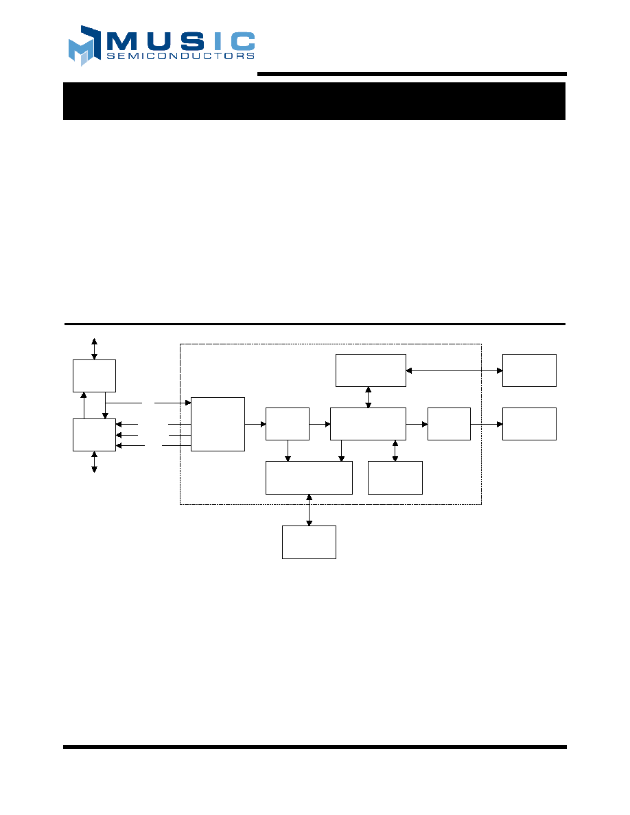
Figure 1: System Application Diagram
Packet
Parser
LANCAM
Interface
Registers
Processor
Interface
Controller
MII and
TAG Port
Result
Port
MII
Processor
ASIC
10/100
PHY
MUSIC
LANCAM
MUSIC
MU9C8338A
10/100
MAC
TAG
FR_ERR
REJECT
MU9C8338A 10/100Mb Ethernet Filter Interface
MU9C8338A 10/100Mb Ethernet Filter Interface
MU9C8338A 10/100Mb Ethernet Filter Interface
MU9C8338A 10/100Mb Ethernet Filter Interface

MU9C8338A 10/100Mb Ethernet Filter Interface
General Description
2
Rev. 0a
GENERAL DESCRIPTION
The MU9C8338A, when configured with the MUSIC
Semiconductors MU9Cx480B family of LANCAMs
provides a high performance, large capacity Ethernet
address processing subsystem for use in Ethernet bridge,
switch, or remote access products. The device is designed
to work in single-port system supporting a 100Mb/s
Ethernet port at wire speed.
OPERATIONAL OVERVIEW
Because of the flexibility of the MU9C8338A, the best
way to approach the feature set of the device is to first
look at a typical 10/100Mb Ethernet application. The
MU9C8338A captures the Destination address (DA) and
the Source address (SA) of an incoming Ethernet frame on
the MII port. After checking for a frame error or collision,
the DA is processed and the result (associated data,
usually a port ID) is made available. The SA then is
checked, and either learned if new, or aged if already in the
list.
Typical MU9C8338A Application
The MU9C8338A plays an integral role in the example of
an Ethernet bridge system, shown in Figure 1.
This system can handle up to 32,768 addresses on a
bidirectional 100Mb Ethernet port by utilizing the
MU9C8338A device and four LANCAMs connected as
shown in Figure 1. The MII bus is "tapped" to collect
packet data as it passes from the Ethernet PHY to the
MAC. That data is processed automatically by the
MU9C8338A/LANCAM combination. The MU9C8338A
transfers the DA and SA to the CAMs for comparison. The
results of MU9C8338A/LANCAM data processing are
available through the Result bus or through the Processor
bus. In addition to the Result bus, there is a serial Tag port
for the MII port to relay the Tag ID to the system for
systems that support Tag switching.
When the DA is processed, the MU9C8338A first checks
if the frame is Unicast, Multicast, or Broadcast. Unicast
frames destined for the same collision domain (visible on
the same switch port as it came in on) are rejected. If the
DA is found in the CAM database, the port ID associated
with it is stored in the Result register. Multicast and
Broadcast frames may also be processed by the system if
the MU9C8338A is configured to do so. When Multicast
is enabled, a default action is configured which causes
frames with unknown group addresses to be processed
correctly. Once processing completes, the Result register
is accessed through the Result port or Processor port.
Provided the frame length is correct, and no errors are
detected, the SA is processed. If the SA exists in the CAM
database, the time stamp and Port ID are updated. If the
SA is not found in the CAM database, the address is
learned automatically, along with its Port ID and the
current time stamp information.
Address processing always has priority over management
routines, such as purging aged entries, inserting permanent
entries, deleting entries, or reading from the CAM
database.

Pin Descriptions
MU9C8338A 10/100Mb Ethernet Filter Interface
Rev. 0a
3
PIN DESCRIPTIONS
Note: All signals are implemented in CMOS technology with TTL levels. Signal names that start with a slash ("/") are active LOW.
Inputs should never be left floating. Refer to the Electrical Characteristics section for more information.
Figure 2: Pinout
MII Interface
Note: The MII interface does not know if the system PHY is operating in Full Duplex, Half Duplex or Loopback mode. Therefore, in
applications that use Half Duplex or Loopback mode, care must be taken to ensure that unnecessary MII frames are not placed on the
interface. It is recommended that only valid Receive Frames are allowed to be sent to the MU9C8338A.
RXD[3:0] (Receive Data, Input, TTL)
RXD[3:0] is the 4-bit MII Receive Data nibble (see
Timing Diagrams: Timing Data for RXD, RX_DV, and
RX_ER).
RX_DV (Receive Data Valid, Input, TTL)
Data Valid is on RX_DV; RX_DV is asserted by the PHY
at the beginning of the first nibble of the data frame and
deasserted at the end of the last nibble of the frame. It
indicates that the data is synchronous to RX_CLK and is
itself synchronous to the clock (see Timing Diagrams:
Timing Data for RXD, RX_DV, and RX_ER).
RX_ER (Receive Error, Input, TTL)
RX_ER indicates a data symbol error in 100Mb/s mode or
any other error that the PHY can detect, even if the MAC is
not capable of detecting that error (see Timing Diagrams:
Timing Data for RXD, RX_DV, and RX_ER).
RX_CLK (Receive Clock, Input, TTL)
RX_CLK is the receive clock recovered from the data by the
PHY. It is equal to 25MHz in 100Base-X mode or 2.5MHz in
10Base-X mode.
CRS (Carrier Sense, Input, TTL)
C arrier sense C RS indicates that the medium is active
(non-idle) and remains asserted during a collision. For Rx or
Tx: CRS is HIGH in 10/100Base-X half-duplex mode; for
Rx it is HIGH in repeater, full-duplex, and loopback modes.
CRS is not synchronized to RX_CLK.
6
12
18
24
30
36
1
42
48
54
60
66
72
78
84
90
96
102
108
144
138
132
126
120
114
/WRITE
/PCSS
PROC_RDY
/ INTR
GND
/RESET
INCR
VDD
/PCS
VDD
D6
D4
GND
A7
A6
A5
A4
A3
A2
A1
A0
VDD
D12
D13
D11
D10
D9
D5
D3
D2
D1
D0
D8
D7
D14
GND
VDD
VDD
GND
TDI
TMS
TCK
NC
NC
NC
NC
NC
NC
NC
NC
NC
NC
TP_SD
TP_DV
GND
NC
/TRST
VDD
RX_ER
RX_CLK
RX_DV
FRX_ER
REJ
GND
RXD3
RXD0
RXD1
RXD2
CRS
COL
TDO
GND
NC
SYSCLK
GND
DQ14
NC
DQ11
DQ10
GND
DQ9
DQ8
DQ7
NC
VDD
DQ5
DQ6
DQ4
DQ3
DQ2
GND
DQ1
DQ0
VDD
/FI
/MI
GND
/EC
/E
/CM
/W
/RESET_LC
NC
D15
VDD
DQ15
DQ13
DQ12
RP2
RP3
GND
RP4
RP5
RP6
VDD
RP7
RP8
RP9
RP10
RP11
RP12
GND
RP13
RP14
RP15
RP_DV
VDD
NC
NC
NC
GND
TST_HLD2
NC
VDD
RP_NXT
RP_SEL
GND
RP0
VDD
NC
SC_ENB
TST_HLD
GND
RP1

MU9C8338A 10/100Mb Ethernet Filter Interface
Pin Descriptions
4
Rev. 0a
COL (Collision, Input, TTL)
Collision detect COL is asserted by the PHY upon
detection of a collision on the medium and remains
asserted as long as the collision persists. It is HIGH in
half-duplex modes and remains HIGH for 1 microsecond
following the end of transmission; it is LOW in
full-duplex mode. It is asserted in response to
signal_quality_error message from the PMA in 10Base-X
Heartbeat mode.
Tag Port Interface
REJ (Reject, Output, TTL)
REJ is the reject packet command issued by the
MU9C8338A. REJ is driven HIGH to reject a data frame,
and can be detected by and responded to by the MAC
device from 2 bit times after SFD to 512 bit times (64 byte
times) after SFD. The REJ signal can be made active
LOW by setting Bit 0 in the SSCFG register. (See Timing
Diagrams: REJ Timing Data.
FRX_ER (Frame Error, Output, TTL)
The Forced Receive Error pins provide the logical OR of
the RX_ER and REJ lines for the MII port (see Timing
Diagrams: Timing Data for FRX_ER in Relation to REJ
and RX_ER).
TP_SD (Tag Port Data, Output, TTL)
The Tag Port Serial Data pin carries the destination Port
ID to external circuitry as soon as it is collected from the
CAM (see Timing Diagrams: Timing Data for Tag Ports
TP_DV and TP_SD).
TP_DV (Tag Port Data Valid, Output, TTL)
The Tag Port Data Valid pin is driven HIGH for as long as
unread data exists for the Destination Port ID. Pin TP_SD
carries the Destination Port ID (6 bits) to external circuitry
as soon as it is collected from the CAM (see Timing
Diagrams: Timing Data for Tag Ports TP_DV and
TP_SD).
Result Port Interface
See Timing Diagrams: Timing Data for Result Port
Interface. Table 1 shows the Result Port bit descriptions.
Note: Although the result data register can also be read through
the processor port, it is important to note that the means of
retrieving the data must be unique. Therefore, if the user is not
using the Result Port Interface, but is reading result data through
the processor port, RP_NXT and RP_SEL should be pulled low.
This ensures that all result data remains in the Result Data
register until read through the processor port. RP_NXT and
RP_SEL should be pulled low to 0 volts through a pull-down
resistor (typically 10k ohms).
RP[15:0] (Result Port Data, Output, Tri-state, TTL)
The Result Port Data carries the results of recently
processed packets detected on the MII port. See Table 1
for details of the Result Port Data bit descriptions. These
are identical to the Result Data register bits.
RP_DV (Result Port Data Valid, Output TTL)
The Result Port Data Valid indicates that the RP port
carries valid packet data. As long as there is valid packet
data, RP_DV will stay HIGH.
RP_NXT (Result Port Next Data, Input, TTL)
The Result Port Next pin brings the next result to the RP
bus if RP_SEL is asserted. If there are no additional results
available, the RP_DV will drop LOW after the time
interval specified in the Result Port Timing specification.
RP_SEL (Result Port Select, Input, TTL)
The Result Port Select pin controls RP[15:0] and
RP_NXT. RP_NXT and RP_SEL are connected by a
logical AND. Therefore, RP_SEL must be HIGH in order
for RP_NXT to bring the next result to the RP bus.
RP_SEL can stay continuously HIGH as long as there is
valid packet data, RP_DV will stay HIGH.
Control Interfaces
See Timing Diagrams: Timing Data for Control Interfaces.
SYSCLK (System Clock, Input, TTL)
CLK is the user-supplied system clock for synchronous
chip operation; its frequency must be 25-50 MHz with
duty cycle between 45 to 55 percent.
/RESET (Reset, Input, TTL)
When system Reset is taken LOW, all internal
state-machines are reset to their initial state and any data is
cleared. All registers are returned to default values.
/RESET is synchronous and should be held LOW for a
minimum of two SYSCLK cycles. The user must set the
LANCAM Segment Control register after asserting
/RESET.
Table 1: Result Port Bit Descriptions
Bit(s)
Description
15:10
6-Bit Source Port ID
9:8
Packet Type: Broadcast = 00, Multicast = 01,
Unicast = 10
7 Match
Found
6:1
6-Bit (if CAM Match Found) Destination Port ID
0
(If Match Found) Destination Port = Source Port

Pin Descriptions
MU9C8338A 10/100Mb Ethernet Filter Interface
Rev. 0a
5
INCR (Increment Time Stamp Counters, Input, TTL)
INCR is a user command to invoke the built-in purge
routine. Both STCURR and STPURG 8-bit counters are
advanced one count on the rising edge of INCR, and the
time stamp stored with each LANCAM entry is compared
with STPURG. Matching entries subsequently are purged
or deleted. This pin must be configured, if it is required, by
setting bit 2 and bit 3 in the System Target (STARG)
register. INCR must be held HIGH for a minimum of one
SYSCLK cycle. Consecutive assertions of INCR must be
a minimum of 8 SYSCLK cycles apart. Each counter can
be incremented individually through the Processor Port.
(see Operational Characteristics: STARG System Target
Register Mapping).
Host Processor Interface
The Host Processor interface is asynchronous to the
System Clock. This interface is controlled by the /PCS or
/PCSS (whichever is appropriate) and PROC_RDY
signals, which form the handshaking between the
processor and the MU9C8338A. This allows the end
system to use a processor that runs at a different clock
speed than the clock required by the MU9C8338A. (see
Timing Diagrams: Timing Data for Host Processor
Interface).
/PCS (Processor Port Chip Select, Input, TTL)
Processor Chip Select is taken LOW by the host processor
to gain access to the MU9C8338A Port or Chip registers.
/PCSS (Processor Port Chip Select System, Input, TTL)
Processor Chip Select System is taken LOW by the host
processor to gain access to the MU9C8338A System
registers or to access the LANCAM.
/WRITE (Processor Port Read/Write, Input, TTL)
Read/Write determines the direction of data flow into or
out of the MU9C8338A host processor interface. If
/WRITE is LOW, the data is written into the register
selected by A[7:0] and /PCS or /PCSS; if HIGH, the data
is read from the register selected by A[7:0] and /PCS or
/PCSS.
A[7:0] (Processor Port Address, Input, TTL)
Processor Address bus A[7:0] selects the MU9C8338A
register accessed by the host processor.
D[15:0] (Processor Port Data, Input/Output, Tri-state,
TTL)
Processor Data bus D[15:0] is the tri-state processor data
bus for the MU9C8338A.
PROC_RDY (Processor Port Ready, Output, Tri-state,
TTL)
When reading from or writing to any MU9C8338A
internal register, the PROC_RDY tri-state output goes
LOW on the falling edge of /PCS or /PCSS. If it is a read
cycle, PROC _RDY goes HIGH on the rising edge of
SYSCLK once data is available. If it is a write cycle,
PROC_RDY goes HIGH on the rising edge of SYSCLK
when the internal register is ready to accept data.
/INTR (Processor Interrupt, Output, TTL)
/INTR goes LOW to signal that one of the two
configurable interrupt conditions have been satisfied. The
two separate conditions are configured by setting bits in
the appropriate register. /INTR returns HIGH when the
appropriate register is read. See Table 2 for details of
which interrupt conditions are possible and which register
must be read to reset the /INTR pin to HIGH.
Table 2: /INTR Settings
Register Required to
Select Interrupt
Condition
To clear /INTR, Read
Interrupt Condition
PTARG
RSTAT. Please note that /INTR will only return
HIGH when all possible result data has been read.
The MII port has parsed an incoming packet. The DA lookup
has been performed and the result data is available to be
read from RDAT register.
STARG
SSTAT. Please note that /INTR will only return
HIGH when the LANCAM has become not full.
Therefore, after the SSTAT register read has
confirmed the status of the interrupt condition, an
entry should be removed from the LANCAM by
using the PURGE sequence.
The /FF output from the LANCAM(s) has indicated that the
LANCAM is full. When reading the SSTAT register, a full
condition is indicated by bit 0 = 0.