Document Outline
- Application Benefits
- Distinctive Characteristics
- General Description
- Operational Overview
- Pin Descriptions
- DQ31Ö0 (Data Bus, Three-state, Common Input/ Output)
- AC12Ö0/AC11Ö0 (Address/Control Bus, Input)
- DSC (Data Segment Control, Input)
- AA12Ö0/AA11Ö0 (Active Address, Output)
- PA3Ö0 (Page Address, Output)
- /E (Chip Enable, Input)
- /CS1, /CS2 (Chip Select 1, Chip Select 2, Inputs)
- /W (Write Enable, Input)
- /OE (Output Enable, Input)
- /AV (Address Valid, Input)
- /VB (Validity Bit, Three-state, Common Input/Output)
- /MF (Match Flag, Output)
- /MI (Match Input, Input)
- /FF (Full Flag, Output)
- /FI (Full Input, Input)
- /MM (Multiple Match, Open Drain Output)
- /RESET
- TCLK (JTAG Test Clock, Input)
- TMS (JTAG Test Mode Select, Input)
- TDI (JTAG Test Data Input, Input)
- TDO (JTAG Test Data Output, Output)
- /TRST (JTAG Reset, Input)
- VDD, VSS (Positive Power Supply, Ground)
- Functional Description
- Operational Characteristics
- Register Descriptions
- Control State Overview
- Control State Descriptions
- Electrical
- Timing Diagrams
- Package
- Ordering Information
Data Sheet
MUSIC Semiconductors, the MUSIC logo, and the phrase "MUSIC Semiconductors" are
March 6, 2001 Rev. 4a
Registered trademarks of MUSIC Semiconductors. MUSIC is a trademark of
MUSIC Semiconductors.
APPLICATION BENEFITS
∑
Longest Prefix Match searches of IPv4 addresses
∑
28 million IPv4 packets per second supports up to 18
Gb Ethernet or 7 OC-48 ATM ports at wire speed
∑
Exact match on MAC addresses
∑
Processes DA and SA within 190 ns, supporting three
ports of 1 Gb or 34 ports of 100 Mb Ethernet at wire
speed
∑
Mixed mode L3 and L2 single search engine for two
ports at 1 Gb or 29 ports of 100 Mb Ethernet at wire
speed
∑
Directly
addresses
external
RAM
containing
associated data of any width
∑
Hardware control states directly address memory and
registers; Instruction and Status registers for optional
software control
DISTINCTIVE CHARACTERISTICS
∑
4K and 8K x 64-bit words
∑
32-bit ternary or 64-bit binary compares
∑
35 ns deterministic compare and output time
∑
32-bit Data I/O port
∑
16-bit Match Address Output port
∑
Address/Control
bus
directly
controls
device
operations for faster operation or higher throughput
∑
Seven selectable mask registers
∑
Synchronous operation
∑
Cascadable for increased depth
∑
Extensive set of control states for flexibility
∑
JTAG interface
∑
100-pin TQFP package; 3.3 Volt operation
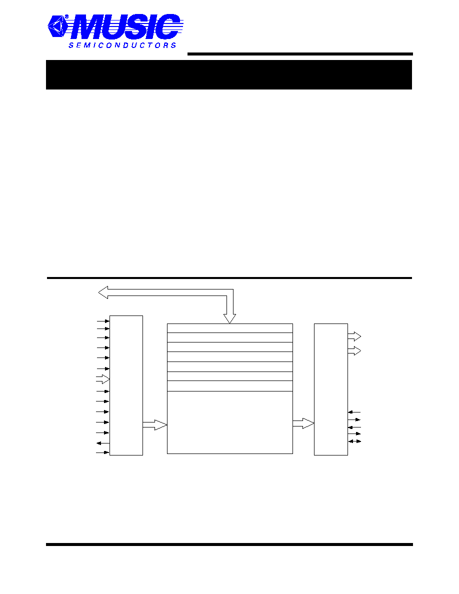
Figure 1: Block Diagram
DQ31≠0
/VB
AA Bus
PA3≠0
/MM
/RESET
TCLK
TMS
TDI
TDO
/TRST
CONTROL
AND
ADDRESS
DECODER
PRIORITY
ENCODER
AND
FLAG
LOGIC
/E
/CS1
/CS2
/W
/OE
/AV
AC Bus
/DSC
INSTRUCTION REGISTER
DEVICE SELECT REGISTER
STATUS REGISTER
CONFIGURATION REGISTER
ADDRESS REGISTER
MASK REGISTERS 1≠7
COMPARAND REGISTER
4 K x 64 Word
(MUAC4K64)
8 K x 64 Word
(MUAC8K64)
Address Database
/M F
/M I
/F F
/FI
MUAC Routing CoProcessor (RCP) Family
MUAC Routing CoProcessor (RCP) Family
MUAC Routing CoProcessor (RCP) Family
MUAC Routing CoProcessor (RCP) Family

MUAC Routing CoProcessor (RCP) Family
General Description
2
Rev. 4a
GENERAL DESCRIPTION
The MUAC RCP family consists of 4K and 8K x 64-bit
Routing CoProcessors (RCPs) with a 32-bit wide data
interface and a 32-bit ternary compare instruction. The
device is designed for use in layer 3 switches, routers, and
layer 2 switches to provide very high throughput address
translation using tables held in external RAM. The MUAC
RCP has a fully deterministic search time, independent of
the size of the list and the position of the data in the list.
This unique feature guarantees that the wire speed address
recognition does not impact the latency or induce some
jitter on the latency of the global system. Address fields
from the packet header are compared against a list of
entries stored in the array. As a result of the comparison,
the MUAC RCP generates an index that is used to access
an external RAM where port mapping data and other
associated information is stored.
A set of control states provides a powerful and flexible
control interface to the MUAC RCP. This control structure
allows memory read and write, register read and write,
data move, comparison, validity control, addressing
control, and initialization operations.
The MUAC RCP architecture uses direct hardware control
of the device and an independent bus for returning match
results. Software control is also supported for systems
where maximum performance is not needed.
OPERATIONAL OVERVIEW
The MUAC RCP is designed to act as an address
translator for lookup tables in layer 3 switches, routers,
and layer 2 switches. Refer to Figure 2 for a simplified
block diagram of a switch. During normal operation, the
controller extracts the address information from an
arriving packet to form the comparand, which is then
compared against the contents of the MUAC RCP. The
MUAC RCP generates an index that is used to access the
data in an external RAM, which holds the destination port
for accessing the network. The controller reads the data
from the RAM and forwards the packet.
A unique feature of the MUAC RCP is its ternary
comparison that processes IPv4 CIDR addresses in a
single cycle. The bits of each MUAC RCP word are
paired, such that each pair can contain two binary values
(0,1) or one ternary (0,1,X= "Don't Care") value. A
ternary value uses two bits, pairing bit n from the first 32
bits (31-0) with bit n+32. When storing a ternary 0 or 1,
the value to be stored is written into bit n (0<=n<=31), and
the complement of the value is written to bit n+32. Thus, a
ternary 0 written to ternary pair 7 would consist of a 0
stored in bit 7 and a 1 stored in bit 39. When storing a
ternary X, 0 is written to both bits in the pair.
Using bit pairs that are 32 bits apart simplifies the
computation of the pair by a processor. Assume that the
ternary value we wish to store is contained in two 32-bit
processor words. Word A contains the value to be stored
and word M contains a mask value, with a 0 in each
position at which an X is to be stored. The value to be
written to bits 31-0 of the MUAC RCP is (A&M) and the
value to be written to bits 63-32 of the MUAC RCP is
(~A&M).
A special instruction, CMPT DQ, performs the ternary
comparison processing for IPv4 CIDR addresses. The data
on the DQ bus are used directly as both the comparand and
compare mask bits 31≠0, and the one's complement of the
DQ bus data are used as both the comparand and compare
mask bits 63≠32. As a result, this instruction matches a
DQ bit of 0 with bit pairs storing both 0 and X, and a DQ
bit of 1 matches bit pairs storing both 1 and X.
IPv4 CIDR addresses are prioritized by placing their
ternary-encoded values into the MUAC RCP memory
such that entries with longer netmasks (longer matches)
have higher priority (lower indices). Thus, when the
MUAC RCP performs a ternary comparison, it will return
the index of the longest matching entry. Typically, the
system is initialized by a processor that writes routing
table information into the MUAC RCP. The index at
which a write takes place is driven onto the PA:AA bus, so
that output port data can be written simultaneously into the
external RAM at the correct index.
The validity of a location in the Address Database is
determined by an extra bit called the Validity bit. This bit is
set and reset either with an index or an associative match.
Therefore, when a new entry is written to the database, its
Validity bit is set valid.
When a database location is deleted, the Validity bit for that
entry is reset, and the index of the location is driven onto
the Active Address bus. This simple mechanism allows
easy maintenance of the tables in both the database and the
external RAM.
The MUAC RCP supports simple daisy chained vertical
cascading that serves to prioritize multiple devices and
provides system-level match and full indication. If the
slight timing overhead associated with the daisy chain is
unacceptable, the MUAC RCP is designed to facilitate
external prioritization across multiple devices.
For layer 2 applications, the MAC addresses are processed
in a binary mode, and the MUAC RCP looks for an exact
match. An MUAC RCP can be used to process both MAC
addresses and IPv4 CIDR in the same device.

Operational Overview
MUAC Routing CoProcessor (RCP) Family
Rev. 4a
3
Figure 2: Switch Block Diagram
Controller
RAM
Switch
Fabric
MUAC
Switch Control
and Packet
Data
Network
Address
Data
RCP
Control
Packet Stream
RAM
Address

MUAC Routing CoProcessor (RCP) Family
Pin Descriptions
4
Rev. 4a
PIN DESCRIPTIONS
Note: Signal names that start with a slash ("/") are active LOW. All signals are 3.3V CMOS level. Never leave inputs floating. The
CAM architecture draws large currents during compare operations, mandating the use of good layout and bypassing techniques. Refer
to the Electrical Characteristics section for more information.
DQ31≠0 (Data Bus, Three-state, Common
Input/ Output)
The DQ31≠0 lines convey data to and from the MUAC
RCP. When the /E input is HIGH the DQ31≠0 lines are
held in their high-impedance state. The /W input
determines whether data flows to or from the device on the
DQ31≠0 lines. The source or destination of the data is
determined by the AC bus, DSC, and the /AV line. During
a Write cycle, data on the DQ31≠0 lines is registered by
the falling edge of /E.
AC12≠0/AC11≠0 (Address/Control Bus,
Input)
When Hardware control is selected, the AC bus conveys
address or control information to the MUAC RCP,
depending on the state of the /AV input. When /AV is
LOW then the AC b us carries an address; when /AV is
HIGH the AC bus carries control information. Data on the
AC bus is registered by the falling edge of /E. When
software control is selected, the state of the AC bus does
not affect the operation of the device.
DSC (Data Segment Control, Input)
When DQ bus access to a 64 bit register or memory word
is performed, the DSC input determines whether bits 31≠0
(DSC LOW) or bits 63≠32 (DSC HIGH) are accessed.
Access to 32 bit registers require that DSC be held LOW.
AA12≠0/AA11≠0 (Active Address, Output)
The AA b us conveys the Match address, the Next Free
address, or Random Access address, depending on the
most recent memory cycle. The /OE input enables the AA
bus; when the /OE input is HIGH, the AA bus is in its
high-impedance state; when /OE is LOW the AA bus is
active. In a vertically cascaded system after a Comparison
cycle, Write at Next Free Address cycle or Read/Write at
Highest-Priority match, only the highest-priority device
will enable its AA bus, regardless of the state of the /OE
input. In the event of a mismatch in the Address Database
after a Compare cycle, or after a Write at Next Free
Address cycle into an already full system, the
lowest-priority device will drive the AA bus with all 1s.
The AA bus is latched when /E is LOW, and are free to
change only when /E is HIGH.
Figure 3: MUAC RCP Pinout
82
83
84
85
86
87
88
89
90
91
92
93
94
95
96
97
98
81
31
10 0
99
33
34
35
36
37
38
39
40
41
42
43
44
45
46
47
48
49
50
32
TCLK
TMS
TDI
DQ0
DQ1
DQ2
DQ3
VDD
DQ4
DQ5
DQ6
DQ7
VSS
DQ8
DQ9
DQ10
DQ11
VDD
DQ12
DQ13
DQ14
DQ15
VSS
VSS
VSS
AC11
AC10
AC9
AC8
AC7
AC6
VDD
AC5
AC4
AC3
AC2
AC1
AC0
TDO
AA12/NC*
80
79
78
77
76
75
74
73
72
71
70
69
68
67
66
65
64
63
62
61
60
59
58
57
56
55
54
53
52
51
DQ16
DQ17
DQ18
DQ19
VDD
DQ20
DQ21
DQ22
DQ23
VSS
DQ24
DQ25
DQ26
DQ27
VDD
DQ28
DQ29
DQ30
DQ31
VSS
/E
/W
/CS1
/CS2
/OE
VSS
/AV
/VB
/
RESET
/TRST
1
2
3
4
5
6
7
8
9
10
11
12
13
14
15
16
17
18
19
20
21
22
23
24
25
26
27
28
29
30
VSS
VSS
AA12/NC*
AA8
VSS
AA7
AA6
AA5
AA4
VDD
AA3
AA2
AA1
AA0
VSS
/MF
/FF
VDD
/M
I
/FI
VSS
/MM
DSC
PA3
PA2
PA1
PA0
AA10
AA9
AA11
MUAC RCP
100-Pin TQFP
(Top View)
* NC on MUAC4K64

Pin Descriptions
MUAC Routing CoProcessor (RCP) Family
Rev. 4a
5
PA3≠0 (Page Address, Output)
The PA3≠0 lines convey Page Address information. When
the /OE input is HIGH, the PA3≠0 outputs are in their
high-impedance state; when /OE is LOW the PA3≠0 lines
carry the Page Address value held in the Configuration
register. The PA3≠0 lines are latched when /E is LOW, and
are free to change only when /E is HIGH. The Page
Address value of the currently active or highest-priority
responding device is output at the same time, and under
the same conditions, as the AA bus is active.
/E (Chip Enable, Input)
The /E input is the main chip enable and synchronizing
control for the MUAC RCP. When /E is HIGH, the chip is
disabled and the DQ31≠0 lines are held in their
high-impedance state. The falling edge of /E registers the
/W, /CS1, /CS2, /AV, /AC bus, DSC, and the /VB and
DQ31≠0 lines for a Write cycle. /E being LOW causes the
results of the previous comparison or memory access to be
latched on the PA:AA bus; when /E goes HIGH the latches
opens allowing the new comparison results or random
access memory address to flow to the PA:AA bus.
/CS1, /CS2 (Chip Select 1, Chip Select 2,
Inputs)
The /CS1 and /CS2 inputs enable the MUAC RCP. If
either /CS1 or /CS2 are LOW, the device is selected for a
Read, Write, or Compare cycle through the DQ31≠0 lines,
or for an internal data transfer. The /CS1 and /CS2 lines do
not have any effect on the PA:AA bus. The state of the
/CS1 and /CS2 lines is registered by the falling edge of /E.
/W (Write Enable, Input)
The /W input determines the direction of data transfer on
the DQ31≠0 lines during Read, Write, and Data Move
cycles. When /W is LOW, data flows into the DQ31≠0
lines; when /W is HIGH, data flows out. The /W line also
conditions the control state present on the AC bus and
DSC lines. The state of the /W line is registered by the
falling edge of /E.
/OE (Output Enable, Input)
The /OE input enables the PA:AA bus. When /OE is
HIGH, PA:AA bus are in their high-impedance state.
When /OE is LOW, PA:AA bus are active, and convey the
results of the last Comparison Cycle Match address or
Memory Access address. In a vertically cascaded system,
only the PA:AA bus of the highest-priority device will be
activated by /OE being LOW; in lower-priority devices,
the PA:AA bus remains in high-impedance regardless of
the state of /OE.
/AV (Address Valid, Input)
When Hardware control is selected, the /AV input
determines whether the AC bus carries address or control
information. When /AV is LOW, the AC bus conveys a
memory address; when /AV is HIGH, the AC bus conveys
control information. The state of the /AV line is registered
by the falling edge of /E. When software control is
selected, the /AV line distinguishes between instructions
and data on the DQ31≠0 lines; when /AV is LOW, data is
present on the DQ31≠0 lines; when /AV is HIGH, an
instruction is present on the DQ11≠0 lines.
/VB (Validity Bit, Three-state, Common
Input/Output)
During accesses over the DQ31≠0 lines, the /VB line
conveys validity information to and from the MUAC RCP.
During a Write cycle (/W=LOW), when /VB is LOW the
addressed location is set valid; when /VB is HIGH it is set
empty. During a Read cycle (/W=HIGH), the validity of
the addressed location is read on the /VB line. During a
Write cycle, the state of the /VB line is registered by the
falling edge of /E.
/MF (Match Flag, Output)
The /MF output indicates whether a valid match has
occurred during the previous Comparison cycle. If the
/MF output is HIGH at the end of a Comparison cycle,
then no match occurred; if it is LOW then either a match
occurred within the device, or the /MI input is LOW,
conditioned by the /MF output from a higher-priority
device in the system. The state of the /MF line will not
change until after the rising edge of /E during the
Comparison cycle. Note that /MF indicates the results of
the most recent Comparison cycle; it will not change when
the PA:AA bus carry an address other than the Match
address.
/MI (Match Input, Input)
The /MI input receives match information from the next
higher-priority MUAC RCP in a vertically cascaded
system to provide system-level prioritization. When the
/MI input is HIGH, the /MF output will only go LOW if
there is a match during a Comparison cycle; when the /MI
input is LOW, the /MF output will go LOW. The /MF
output from one device is connected to the /MI input of the
next lower-priority device. The /MI pin of the
highest-priority device must be tied HIGH.