 | –≠–ª–µ–∫—Ç—Ä–æ–Ω–Ω—ã–π –∫–æ–º–ø–æ–Ω–µ–Ω—Ç: CS6703 | –°–∫–∞—á–∞—Ç—å:  PDF PDF  ZIP ZIP |
3UHOLPLQDU\
200Mbps Fiber-Optic VCSEL/Laser Driver
CS6703
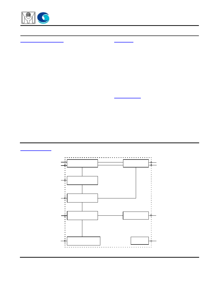
BLOCK DIAGRAM
GENERAL DESCRIPTION
Myson-Century Technology
FEATURES
APPLICATIONS
USA:
4020 Moorpark Avenue Suite 115
San Jose, CA, 95117
Tel: 408-243-8388 Fax: 408-243-3188
sales@myson.com.tw
www.myson.com.tw
Rev.0.6 January 2002
page 1 of 7
Myson-Century Technology, Inc.
Taiwan:
No. 2, Industry East Rd. III,
Science-Based Industrial Park, Hsin-Chu, Taiwan
Tel: 886-3-5784866 Fax: 886-3-5784349
The CS6703 is a high-speed fiber optic VCSEL
driver ideally suited for applications up to 400Mbps.
The CS6703 is programmable and has fully
differential PECL data inputs and CMOS control
inputs.
The bias and modulation current of the CS6703
can be set independently via two external resistors;
the rise/fall times can also be adjusted using external
resistors.
Normally the CS6703 is direct coupled to PECL
inputs, however if AC coupling is desired, a 2/3 V
DD
bias point is recommended for operation. Please
refer to the application schematic for more details.
∑ Rise/fall time < 700ps, suitable for applications up
to 400Mbps.
∑ Independently programmable laser bias and mod-
ulation current: bias current to 60mA and modula-
tion current to 40mA.
∑ Differential PECL inputs.
∑ Programmable rise/fall times.
∑ Supports both 3.3 and 5 Volt operation.
∑ Available as die or QSOP-16 package.
DINP
DINN
PREDRIVER
MODP
DCB
IXMT
MODN
ROFS
RMOD
RDCB
DCBIAS DRIVER
MODULATION SET
CONTROL LOGIC
BIAS SET
OUTPUT DRIVER
ENABLE
IBIAS
BANDGAP
VREF
RISE/FALL SET
CS6703
∑ FDDI
∑ SDH STM-1
∑ SONET OC-3
∑ Fast Ethernet
∑ Fiber Channel 100
∑ 155 Mbps ATM
∑ 155 Mbps SDH/SONET
∑ VCSEL Driver Transmitters

3UHOLPLQDU\
CS6703
page 2 of 7
Myson-Century Technology
DIE CONNECTION DIAGRAM
Figure-1
PIN CONNECTION DIAGRAM
Figure-2 QSOP-16
RMOD
RDCB
V
DDO
ENABLE
V
DDO
1672
µ
m
2020
µ
m
DINP
ROFS
VREF
V
SSA
V
SSA
DINN
DCB
V
SSO2
MODN MODP
V
SSO1
V
SSB
V
DDA
V
SSB
V
DDA
DINP
DINN
V
SSA
VREF
RMOD
RDCB
ROFS
V
DDO
V
SSO1
MODP
MODN
V
SSO2
DCB
V
SSB
ENABLE
16
15
14
13
12
11
10
9
1
2
3
4
5
6
7
8
CS6703

3UHOLPLQDU\
CS6703
page 3 of 7
Myson-Century Technology
PIN DESCRIPTION
Name
Pin
Description
V
DDA
1
Input section V
cc
pin. Connect to most positive supply voltage.
DINP
2
Differential data input pin. Complementary to pin DINN.
DINN
3
Inverse Differential data input pin. Complementary to pin DINP.
V
SSA
4
Input section ground pin. Connect to most negative supply voltage.
VREF
5
Reference voltage output pin (approximately 1.8V). Connect a capacitor between this pin and
ground.
RMOD
6
Laser modulation current input set pin. Connect a resistor between this pin and ground.
RDCB
7
Laser bias current input set pin. Connect a resistor between this pin and ground.
ROFS
8
Rise/fall time set point input pin. Connect a resistor which is not less than 10k
between this pin
and ground, or leave as an open circuit.
ENABLE
9
Enable input pin (TTL active high).
V
SSB
10
Output section ground pin. Connect to most negative supply voltage.
DCB
11
Laser DC bias current pin.
V
SSO2
12
Output section ground pin. Connect to most negative supply voltage.
MODN
13
Inverse driver output stage pin. See application schematic.
MODP
14
Driver output stage pin. See application schematic.
V
SSO1
15
Output section ground pin. Connect to most negative supply voltage.
V
DDO
16
Output section power pin. Connect to most positive supply voltage.

3UHOLPLQDU\
CS6703
page 4 of 7
Myson-Century Technology
FUNTIONAL DESCRIPTION
CS6703 consists of a laser bias generator, a modulation current driver, and a rise/fall time adjustment circuit.
Laser bias driver
The laser bias current is adjusted by a resistor Rdcb
set
which is connected between pin RDCB and ground.
I
bias
= 210/Rdcb
set
: for 3.3V.
I
bias
= 220/Rdcb
set
: for 5V.
Modulation Current driver
The modulation current is adjusted by a resistor Rmod
set
which is connected between pin RMOD and ground.
I
mod
= 436/Rmod
set
: for 3.3V.
I
mod
= 477/Rmod
set
: for 5V.
Rise/fall time adjustment
The rise/fall time of the CS6703 can be adjusted by a resistor R
offset
which is connected between pin ROFS and
ground.
Figure-3 R
offset
V.S. Rise/Fall time
90k
700
690
680
670
660
650
640
R
ofsset
(
)
ps
6k
20k
30k
40k
70k
80k
60k
50k
10k 15k
Time
Resistance

3UHOLPLQDU\
CS6703
page 5 of 7
Myson-Century Technology
ABSOLUTE MAXIMUM RATINGS
RECOMMENDED OPERATING CONDITIONS
ELECTRICAL CHARACTERISTICS
Symbol
Parameter
Rating
Unit
V
CC
Power supply (V
CC
- Gnd)
6
V
T
a
Operating ambient
-40 to +85
∞
C
T
stg
Storage temperature
-65 to +150
∞
C
Symbol
Parameter
Rating
Unit
V
CC
Power supply (V
CC
- Gnd)
3 to 5.5
V
T
a
Operating ambient temperature
-40 to +85
∞
C
Symbol
Parameter
Min
Typ
Max
Unit
Ibias
Range of programmable laser bias current
-
-
60
mA
Imod
Range of programmable modulation current
-
-
45
mA
Vih
PECL input high
-
V
CC
- 0.95
-
V
Vil
PECL input low
-
V
CC
- 1.75
-
V
I
CC
Supply current
-
Imod+Ibias
+15
-
mA
Tr/Tf
Rise/fall time
-
700
-
ps