 | –≠–ª–µ–∫—Ç—Ä–æ–Ω–Ω—ã–π –∫–æ–º–ø–æ–Ω–µ–Ω—Ç: MTD907 | –°–∫–∞—á–∞—Ç—å:  PDF PDF  ZIP ZIP |
MYSON
TECHNOLOGY
MTD907
Ethernet Encoder/decoder and 10BaseT
Transceiver with Built-in Waveform Shaper
This datasheet contains new product information. Myson Technology reserves the rights to modify the product specification without notice.
No liability is assumed as a result of the use of this product. No rights under any patent accompany the sale of the product.
MTD907 Revision 4.5 01/23/1997
1/14
FEATURES
∑
Pin-out and functionally compatible with Level One LXT907.
∑
Built-in UTP waveform shaping function - no external filters required.
∑
Integrated Manchester encoder/decoder.
∑
10Base-T compliant transceiver and AUI transceiver.
∑
Full duplex capability.
∑
Automatic and manual interface selection (AUI/TP).
∑
Automatic TP polarity detection and correction.
∑
Heartbeat enable/disable function and jabber disable function.
∑
Drives 4 LED status indicators.
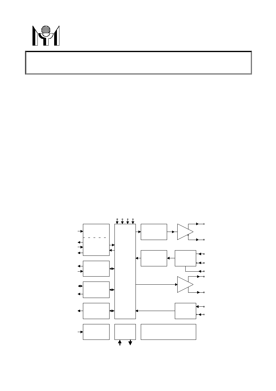
GENERAL DESCRIPTION
MTD907 is an integrated Ethernet Endec and 10Base-T transceiver with built-in UTP transmission waveform
shaping function. The integrated encoder/decoder conforms to IEEE802.3 standards and provides all needed
active circuitry with which to interface the majority of IEEE802.3-conforming controllers to either the 10Base-T
media or attachment unit interface (AUI). The functions provided by MTD907 include Manchester
encoding/decoding, jabber detection, automatic media selection, reception squelch and transmission
waveform shaping, automatic UTP polarity detection and correction for the UTP media.
BLOCK DIAGRAM
COLLISION
LOGIC
LED/STATUS
LOGIC
REMOTE
SIGNALING
TEST LOGIC
XCAL
OSC
MEDIA
SELECTION
AND
CONTROL
WAVEFORM
SHAPING
LINKTEST
POLARITY
DETECT
AMP
AC/DC
SQUELCH
AMP
AC/DC
SQUELCH
REFERENCE Circuit
MODE
CONTROL
MANCHESTER
CODER/
DECODER
MD0, MD1
TXC
TXC, TXE
CRS, RXC,
RXD
COL, JAB
DSQ
LEDR, LEDL,
LEDC, LEDT
JAB, PLR
RLD,
RJAB,
RCMPT
TST
TRST
LBK
AUT
PAULTE
X2
X1
DIP, CIP
DIN, CIN
DOP
DON
RDP
RDN
NTH
TPA, TPB
TNA, TNB

MYSON
TECHNOLOGY
MTD907
MTD907 Revision 4.5 01/23/1997
2/14
1.0 PIN CONNECTION
44-pin PLCC
MTD907
44-pin PLCC
RDN
RDP
DSQ
TNB
TNA
VDD2
VSS2
TP A
TP B
PLR
RJAB
RLD
LTE
JAB
TST
TXC
TXD
TXE
X1
X2
COL
AUT
MD1
MD0
NTH
CIN
CIP
VDD1
DON
DOP
DIN
DIP
PAU
LEDR
LEDT
LEDL
LEDC
LBK
VSS1
TRST
RCMPT
RXD
CRS
RXC
6 5 4 3 2 1 44 43 42 41 40
7
8
9
10
11
12
13
14
15
16
17
39
38
37
36
35
34
33
32
31
30
29
18 19 20 21 22 23 24 25 26 27 28
1.0 PIN DESCRIPTIONS
No
Symbol
I/O
Name
Description
1
34
VDD1
VDD2
-
Positive Power
Supply
+5 Volt power supplies.
2
3
CIP
CIN
I
I
Collision Input
Pair
AUI transceiver CI circuit differential input pair.
4 NTH
I
Normal
Threshold
Active high input, selects normal TP input threshold;
when NTH=0, the TP input threshold is reduced 4.5dB.
5
6
MD0
MD1
I
I
Mode
Selection
Mode selection pins. Determines controller compatibility
mode: mode 00 is for AMD, 01 for Intel, 10 for Fujitsu, 11
for NSC.
7 RLD
O
Remote Link
Down
Active high output. Signifies when the remote port is in
link down condition.
8 LTE
I
Link Test
Enabler
Active high input. Enables the link test when high; when
low, disables the TP link test.
9 JAB
O
Jabber
Indicator
Active high output. High output indicates jabber
condition.
10 TST
I
Test
Active high input internally pulled low. This pin is used in
test mode only.
11 TXC
O
Transmit Clock 10 MHz clock output. Should be directly connected to
the controller to synchronize transmission operation.
12 TXD
I
Transmit Data
Input signal, NRZ data from the controller.
13 TXE
I
Transmission
Enabler
Active high input. Enables data transmission and begins
jabber timer; should be synchronized with TXC by the
controller.
14
15
X1
X2
O
I
Crystal
Oscillator
Built-in crystal oscillator. A 20 MHz crystal must be
connected across these 2 pins or an external clock must
be applied to X2 with X1 left open.
16 COL
O
Collision
Detection
Output signal; drives controller collision detection input.

MYSON
TECHNOLOGY
MTD907
MTD907 Revision 4.5 01/23/1997
3/14
17 AUT
I
Automatic Port
Selection
Active high input. When active, MTD907 defaults to the
AUI port if the TP link test fails. If driven low, the port
selection is determined by the PAU pin.
18 LEDR/
JABDIS
O
I
Receive LED,
Disable Jabber
Active low output driver for receiving the LED indicator.
The LED 'on' time is extended by at least 80 ms.
When externally tied or driven low, disables the internal
jabber timer.
19 LEDT/
PWDN
O
I
Transmit LED,
Power Down
Active low output driver for LED transmission indicator.
The LED 'on' time is extended by at least 80ms.
When externally tied or driven low, forces MTD907 into
power-down state.
20 LEDL/
LPSS
O
I
Link LED,
Link Pass
Active low output driver for link integrity LED indicator.
When externally tied or driven low, forces MTD907 into
'link pass' state.
21 LEDC/
FDX
O
I
Collision LED,
Full Duplex
Active low output driver for collision indicator LED. The
LED on time is extended by at least 80 ms.
When externally tied low, enables MTD907 for full duplex
operation by disabling internal TP loopback and TP
collision detection functions.
22 LBK
I
Loopback
Active high input; enables internal loopback mode.
23
33
VSS1
VSS2
-
Negative
Power Supply
Power supply ground.
24 TRST
I
Test Mode
Reset
Active high test mode reset signal. Only recognized in
test mode (TST pin high) and internally pulled low.
25 RCMPT
O
Remote
Compatible
Active high output; indicating TP transceiver at the
remote end is compatible with remote signaling.
26 RXD
O
Received Data
Output signal; recovers received data. Should be
connected directly to controller.
27 CRS
O
Carrier Sense
Output signal; detects incoming network traffic. Should
be connected directly to controller.
28 RXC
O
Received
Clock
Output signal; recovers received clock. Should be
connected directly to controller.
29 RJAB
O
Remote
Jabber
Active high output signal; indicates when the remote end
is in jabber state.
30 PLR
O
Polarity
Reversal
Active high output signal; indicates when the TP polarity
is reversed.
31
32
35
36
TPB
TPA
TNA
TNB
O
O
O
O
Twisted-pair
Transmission
Pairs A & B
Two differential driver pairs (A and B) for the TP cable.
The outputs are pre-equalized, thus no external filters
are required. The TPX pins and TNX pins must be
shorted together with a 24.9W 1% to match the 100W TP
impedance.
37 DSQ
I
Disable SQE
Active high input. When driven high, selects MTD907 for
hub/switch/repeater operation by disabling signal quality
test (heartbeat).
38
39
RDP
RDN
I
I
Receive Data
Input Pair (TP)
Differential input pair for TP cable. The reception filter is
integrated on-chip. No external filter is required.
40 PAU
I
Select
Port/AUI
Recognized only if the AUT pin is low. PAU=1 selects
AUI port, PAU=0 selects TP port. It is recommended
that you tie this pin to ground if driving AUT pin high.
41
42
DIP
DIN
I
I
AUI Reception
Pair
Differential input pair from the AUI transceiver DI circuit.
43
44
DOP
DON
O
O
AUI
Transmission
Pair
Differential output pair to the AUI transceiver DO circuit.

MYSON
TECHNOLOGY
MTD907
MTD907 Revision 4.5 01/23/1997
4/14
2.0 CONTROLLER COMPATIBILITY MODE DESCRIPTIONS
Mode
Controllers:
MD0
MD1
1
Advanced Micro Devices AM7990 or compatible controllers.
0
0
2
Intel 82586 or 82596, or compatible controllers.
0
1
3
Fujitsu MB86950 or MB86960, Seeq 8005 or compatible continuous
clock-type controllers.
1
0
4
National Semiconductor 8390, TI TMS380C26 or compatible controllers.
1
1
3.0 ABSOLUTE MAXIMUM RATINGS
DC Supply Voltage (Vcc)
-0.5V to +7V
DC Input Voltage (Vin)
-0.5V to Vcc+0.5V
Storage Temperature
-65
o
C to 150
o
C
Operating Temperature
0
o
C to 70
o
C
4.0 OPERATING CONDITIONS
Parameter
Symbol
Min
Typ
Max
Unit
Test Conditions
Power Supply Voltage
Vcc
4.75
5
5.25
V
Operating Temperature
Top
0
-
70
o
C
Icc
-
35
55
mA
Idle
Icc
-
60
80
mA
Transmitting on TP
Icc
-
50
70
mA
Transmitting on AUI
Supply Current
Icc
-
3
6
mA
Power-down mode
5.0 ELECTRICAL CHARACTERISTICS (under operating conditions)
Parameter
Symbol
Min
Typ
Max
Unit
Test Conditions
Input Low Voltage
V
IL
-
-
0.8
V
Input High Voltage
V
IH
2.0
-
-
V
Output Low Voltage
V
OL
-
-
0.4
V
Iol=1.6mA
Output High Voltage
V
OH
2.4
-
-
V
Iol=40uA
Output Low Voltage (LED)
V
OL
-
-
0.7
V
Iol=10mA
T
R
-
3
12
ns
Cload=20pF
Output Rise Time (TXC, RXC)
T
R
-
2
8
ns
TTL load
T
F
-
3
12
ns
Cload=20pF
Output Fall Time (TXC, RXC)
T
F
-
2
8
ns
TTL load
X2 Rise Time (external clock)
-
-
-
10
ns
X2 Duty Cycle (external clock)
-
-
50/50
40/60
%
6.0 AUI ELECTRICAL CHARACTERISTICS (under operating conditions)
Parameter
Symbol
Min
Typ
Max
Unit
Test Conditions
Input Low Current
I
L
-
-
-700
uA
Input High Current
I
H
-
-
500
uA
Differential Output Voltage
V
OD
550
-
1200
mV
Differential Squelch Threshold
V
DS
150
220
350
mV
5 MHz square wave

MYSON
TECHNOLOGY
MTD907
MTD907 Revision 4.5 01/23/1997
5/14
7.0 TP ELECTRICAL CHARACTERISTICS (under operating conditions
)
Parameter
Symbol
Min
Typ
Max
Unit
Test Conditions
Transmit Output Impedance
Zout
-
5
-
W
Peak Differential Output
Voltage
Vod
3.3
3.5
3.7
V
Load=100 W
Transmit Timing Jitter
Addition
-
-
6.4
10
+/-
ns
Internal MAU
Transmit Timing Jitter
Added by MAU and PLS
Sections
-
-
3.5
5.5
+/-
ns
After IEEE 802.3-
specified TP line model
Receive Input Impedance
Zin
-
20
-
kW
Between input pairs
Vds
300
420
585
mV
5MHz square wave
input, NTH=1
Differential Squelch
Threshold
Vds
180
250
345
mV
5MHz square wave
input, NTH=0
8.0 SWITCHING CHARACTERISTICS (under operating conditions)
Jabber Timing:
Parameter
Symbol
Min
Typ
Max
Unit
Maximum Transmission Time before Jabber
-
20
-
150
ms
Unjab Time
-
250
-
750
ms
Link Integrity Pulse Timing:
Parameter
Symbol
Min
Typ
Max
Unit
Link Loss Time
-
63
-
64
ms
Transmit Link Integrity Timing
-
8
-
24
ms
Receive Link Integrity Pulse Timing
-
3.1
-
63
ms
Start-of-Frame Timing, AUI
Parameter
Symbol
Min
Typ
Max
Unit
Decoder Acquisition Time
t
DATA
-
700
1100
ns
CD Turn-on Delay
t
CD
-
50
200
ns
Start-of-Frame Timing, TP
Parameter
Symbol
Min
Typ
Max
Unit
Decoder Acquisition Time
t
DATA
-
1000
1700
ns
CD Turn-on Delay
t
CD
-
400
550
ns
RXC Timing
Parameter
Symbol
Typ
Mode
1
Mode
2
Mode3
Mode
4
Unit
Receive Data Setup from RXC
t
RDS
Min.
43
30
30
30
ns
Receive Data Hold from RXC
t
RDH
Min.
10
30
30
30
ns
RXC Shut-off Delay from CRS
Assertion
t
SWS
Typ.
-
-
+/-100
-
ns
RXC Hold after CRS Turn-off
t
RCH
-
8
1
-
8
bt
RXD Data through Delay
t
RD
Max.
400
375
375
375
ns
CRS Turn-off Delay
t
CRSOFF
Max.
500
475
475
475
ns
RXC Switching Delay after CD Off
t
SWE
Typ.
-
-
120
-
ns

MYSON
TECHNOLOGY
MTD907
MTD907 Revision 4.5 01/23/1997
6/14
Transmission Timing
Parameter
Symbol
Min
Typ
Max
Unit
TXE Setup from TXC
t
EHCH
22
-
-
ns
TXD Setup from TXC
t
DACH
22
-
-
ns
TXE Hold from TXC
t
CHEL
5
-
-
ns
TXD Hold from TXC
t
CHDU
5
-
-
ns
Transmission Start-up Delay, AUI
t
STUD
-
200
450
ns
Transmission Start-up Delay, TP
t
STUD
-
350
450
ns
Transmission through Delay, AUI
t
TPD
-
-
300
ns
Transmission through Delay, TP
t
TPD
-
-
350
ns
COL and Loopback Timing
Parameter
Symbol
Min
Typ
Max
Unit
COL Turn-on Delay
t
COLD
-
-
500
ns
COL Turn-off Delay
t
COLOFF
-
-
500
ns
COL (SQE) Delay after TXE Off
t
SQED
0.65
-
1.6
us
COL (SQE) Pulse Duration
t
SQEP
500
-
1500
ns
LBK Setup from TXE
t
KHEH
10
25
-
ns
LBK Hold after TXE
t
KHEL
10
0
-
ns
9.0 TIMING DIAGRAM
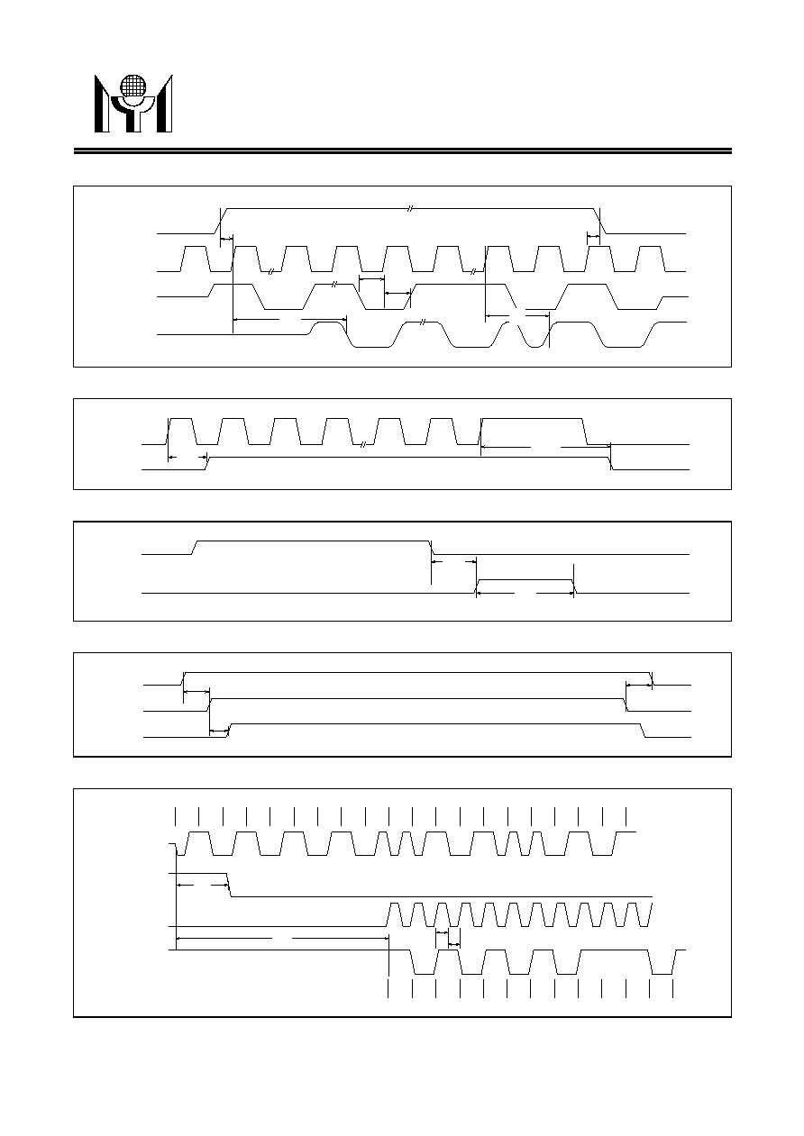
Mode 1, RXC - Start of Frame Timing
1
0
1
0
1
0
1
0
1
1
1
0
1
0
0
0
1
0
1
0
TPIP/TPIN
or DIP/DIN
CRS
RXC
RXD
t
DATA
1
0
1
0
1
0
1
1
1
0
1
1
0
t
RDS
t
RDH
t
CRS
Mode 1, RXC - End of Frame Timing
1
0
1
0
1
0
1
0
0
1
0
1
0
1
0
1
0
0
t
RD
t
CDOFF
t
RCH
TPIP/TPIN
or DIP/DIN
CRS
RXC
RXD
MYSON
TECHNOLOGY
MTD907
MTD907 Revision 4.5 01/23/1997
7/14
Mode 1, Transmission Timing
t
EHCH
t
STUD
t
DSCH
t
TPD
t
CHEL
TXE
TXC
TXD
TPO
t
CHDU
Mode 1, Collision Detection Timing
t
COLD
t
COLOFF
CI
COL
Mode 1, HBT/CI Output Timing
t
SQED
t
SQEP
TXE
COL
Mode 1, Loopback Timing
t
KHEL
t
CAEA
t
KHEH
LBK
TXE
CRS
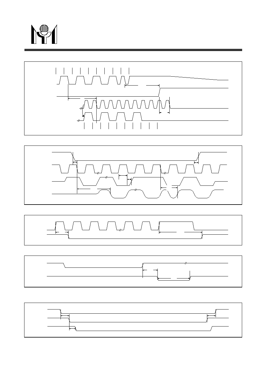
Mode 2, RXC - Start of Frame Timing
1
0
1
0
1
0
1
0
1
1
1
0
1
0
0
0
1
0
1
0
TPIP/TPIN
or DIP/DIN
CRS
RXC
RXD
t
DATA
1
0
1
0
1
0
1
1
1
0
1
1
0
t
RDS
t
RDH
t
CRS
MYSON
TECHNOLOGY
MTD907
MTD907 Revision 4.5 01/23/1997
8/14
Mode 2, RXC - End of Frame Timing
1
0
1
0
1
0
1
0
0
1
0
1
0
1
0
1
0
0
t
RD
t
CDOFF
t
RCH
TPIP/TPIN
or DIP/DIN
CRS
RXC
RXD
Mode 2, Transmission Timing
t
EHCH
t
STUD
t
DSCH
t
TPD
t
CHEL
TXE
TXC
TXD
TPO
t
CHDU
Mode 2, Collision Detection Timing
t
COLD
t
COLOFF
CI
COL
Mode 2, HBT/CI Output Timing
t
SQED
t
SQEP
TXE
COL
Mode 2, Loopback Timing
t
KHEL
t
CAEA
t
KHEH
LBK
TXE
CRS

MYSON
TECHNOLOGY
MTD907
MTD907 Revision 4.5 01/23/1997
9/14
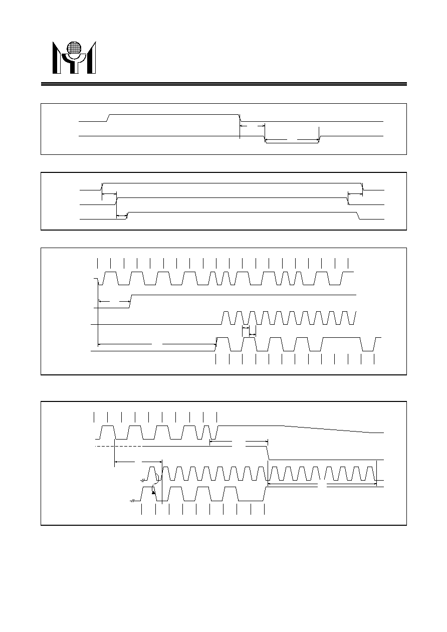
Mode 3, RXC - Start of Frame Timing
1
0
1
0
1
0
1
0
1
1
1
0
1
0
0
0
1
0
1
0
TPIP/TPIN
or DIP/DIN
CRS
RXC
RXD
t
DATA
1
0
1
0
1
0
1
1
1
0
1
1
0
t
RDS
t
RDH
t
CRS
t
SWS
Generated form TCLK
Recovered form Input Data Stream
Mode 3, RXC - End of Frame Timing
1
0
1
0
1
0
1
0
0
1
0
1
0
1
0
1
0
0
t
RD
t
CDOFF
t
SWE
TPIP/TPIN
or DIP/DIN
CRS
RXC
RXD
Recovered Clock
Generated from TXC
Mode 3, Transmission Timing
t
EHCH
t
STUD
t
DSCH
t
TPD
t
CHEL
TXE
TXC
TXD
TPO
t
CHDU
Mode 3, Collision Detection Timing
t
COLD
t
COLOFF
CI
COL
MYSON
TECHNOLOGY
MTD907
MTD907 Revision 4.5 01/23/1997
10/14
Mode 3, HBT/CI Output Timing
t
SQED
t
SQEP
TXC
COL
Mode 3, Loopback Timing
t
KHEL
t
CAEA
t
KHEH
LBK
TXE
CRS
Mode 4, RXC - Start of Frame Timing
1
0
1
0
1
0
1
0
1
1
1
0
1
0
0
0
1
0
1
0
TPIP/TPIN
or DIP/DIN
CRS
RXC
RXD
t
DATA
1
0
1
0
1
0
1
1
1
0
1
1
0
t
RDS
t
RDH
t
CRS
Mode 4, RXC - End of Frame Timing
1
0
1
0
1
0
1
0
0
1
0
1
0
1
0
1
0
0
t
RD
t
CDOFF
t
RCH
TPIP/TPIN
or DIP/DIN
CRS
RXC
RXD

MYSON
TECHNOLOGY
MTD907
MTD907 Revision 4.5 01/23/1997
11/14
Mode 4, Transmission Timing
t
EHCH
t
STUD
t
DSCH
t
TPD
t
CHEL
TXE
TXC
TXD
TPO
t
CHDU
Mode 4, Collision Detection Timing
t
COLD
t
COLOFF
CI
COL
Mode 4, HBT/CI Output Timing
t
SQED
t
SQEP
TXE
COL
Mode 4, Loopback Timing
t
KHEL
t
CAEA
t
KHEH
LBK
TXE
CRS
10.0 FUNCTIONAL DESCRIPTION
MTD907 is an Ethernet Endec and 10BaseT transceiver with a built-in waveform shaper that performs the
Media Attachment Unit (MAU) and Physical Layer Signaling (PLS) functions as defined in the IEEE802.3
specification.
MTD907 can function as either a PLS-only device interfacing a supported controller to an AUI cable or as an
integrated PLS/MAU interfacing a supported controller to the TP cable. In the following functional descriptions,
aII functions are defined as seen from the controller side of the interface.
Controller Compatibility
MTD907 is configurable for interfacing with common industrial standard Ethernet controllers. The mode
selection pins, MD0 and MD1, provide the mode configuration capability as tabulated in Section 2.0. The timing
specification of different controller modes is specified in Section 8.0's RXC timing. Applicable timing diagrams
for each of the supported controller modes are included in Section 9.0.

MYSON
TECHNOLOGY
MTD907
MTD907 Revision 4.5 01/23/1997
12/14
Transmission Function
MTD907 samples TXD data from the controller at the rising edge of the TXC signal and then performs the
Manchester encoding on the input data stream. The encoded data is then transmitted through either the AUI
port or the TP cable network . The built-in waveform-shaping circuits produce pre-distorted TP output
waveform comforming to the jitter template specified in IEEE802.3. No external filter is required in MTD907
applications. If LTE is enabled and the TP port is selected as the network media, MTD907 transmits link
integrity test pulses at regular intervals during idle periods. Due to its voltage drive and TP output drivers' low
output impedence, the driving end source resistance is decided by external resistors.
Jabber Control Function
The jabber control function of MTD907 closely follows the IEEE 802.3 specification. The MTD907 built-in
watchdog timer prevents the DTE from continuous transmission. When the TXE input is asserted for longer
than the time limit, both transmission and loopback functions are disabled, and the JAB output pin will be
asserted. Once MTD907 enters the jabber state, it will exit it only if the TXE signal remains idle for a period of
250-750ms.
The jabber function of MTD907 can be disabled by externally pulling the LEDR pin low.
SQE Function
MTD907 supports the signal quality error (SQE) function, which can be disabled through DSQ input. If the SQE
function is enabled (DSQ=0), MTD907 will transmit the SQE signal after every successful 10BaseT
transmission. This SQE signal will be a 10 +/- 5 bit time assertion of the COL output pin. If the AUI port is
selected as the transmission media, the SQE is determined by the external MAU.
When using MTD907 in hub or switch applications, the SQE function must be disabled (DSQ=1).
Reception Function
MTD907's reception function recovers both the clock and data from the incoming Manchester-encoded data
stream from either the AUI or TP port. The recovered clock and data are sent to the controller through the RXC
and RXD pins, respectively.
Internal filter and squelch functions are integrated in MTD907 in order to discriminate noise from valid TP
signals. No external reception filter is needed. If the incoming signal from either the AUI or TP input exceeds
the squelch requirements, the CRS pin will be asserted and internal timing recovery circuits will be activated. A
fast lock-on PLL will typically lock on to the input signal in 5-bit time. If the input signal drops below the squelch
threshold or signal transitions are absent for 8-bit time (typical), the internal circuit will return to its idle state.
TP Interface Polarity Correction Function
The MTD907 TP interface polarity correction function detects and corrects TP polarity error using both TP link
pulses and end-of-frame data. The TP polarity is internally decided as being reversed only if 8 consecutive link
pulses or end-of-frame data are received with a polarity opposite to the expected polarity. Upon detecting TP
polarity reversal, MTD907 will automatically exchange the received TP data polarity. This correction function is
always active.
Collision Detection Function
The collision detection function is applicable only if MTD907 is used as PLS/MAU in a standard 10BaseT
network. A collision is detected if valid data is present simultaneously on both TP transmission and TP
reception circuits. MTD907 reports this to the controller via the assertion of the COL output. If MTD907 is used
as PLS only, i.e. external MAU, then the collision detection is based on valid signals from the AUI port.
If MTD907 is configured to function as a full-duplex TP transceiver by externally pulling the LEDC pin low, the
collision detection function for TP will be disabled internally. Also, if the MTD907 LBK pin is driven high, all
collision function is disabled.
Loopback Function

MYSON
TECHNOLOGY
MTD907
MTD907 Revision 4.5 01/23/1997
13/14
MTD907 has 4 different loopback modes. If the TP port and half-duplex mode are selected, MTD907 provides
the normal loopback function as defined in 10BaseT standards. If the TP port and full-duplex mode are
selected, the internal loopback is disabled, allowing external loopback through TP ports. If the AUI interface is
selected and LBK=0, the external AUI loopback mode is in effect. If LBK is driven high, the internal collision
detection function is disabled, and the transmission data is forced to loop back through internal Manchester
ENDEC with disregard as to which interface port is selected.
Link Integrity Test
The MTD907 link integrity test is implemented as specified in IEEE802.3 10BaseT standards. This function is
enabled when input pin 8 (LTE) is driven high. While LTE=1, MTD907 will recognize link integrity pulses
received in absence of a valid TP data packet. If both link integrity pulses and TP data packets are not detected
within 65-66ms, MTD907 will enter a link-fail state and will disable the transmission and normal loopback
functions. After it enters such a state, MTD907 will exit the link-fail state if one valid TP packet or 2 or more link
integrity pulses are received. Link integrity pulses received within an interval of 4ms will be ignored by MTD907.
Remote Signaling
The link integrity pulses transmitted by MTD907 include encoded local status information by varying the link
pulse intervals. This feature is implemented in such a way that MTD907 is compatible with any chip that uses
the same signaling scheme, such as many of the Level One products.
Three different pieces of status information are encoded and are described as follows. Local link-down is
encoded as link pulse interval sequences of 10ms-15ms-20ms. Local jabber is encoded as link pulse interval
sequences of 10ms-20ms-15ms. Remote-signaling capability is encoded as a link pulse interval sequence of
10ms-20ms. MTD907 will detect and decode link pulses, thus encoding and reporting them through the RLD,
RJAB and RCMPT output pins, respectively.
11.0 Comparison of MTD907 and Level One LXT901/LXT907
Waveform Synthesis Method
The main difference between MTD907 and Level One LXT901/LXT907 is the waveform synthesis method used.
Level One products use a table-look-up method with a 5-bit DAC operating at 70MHz. MTD907 uses a delay
cell based 16-tab FIR filter operating at 160MHz to synthesize the pre-distorted transmission waveforms
required by 10BaseT standards with much refined waveform.
Mode1 and Mode4 End-of-Frame RXC Timing
Eight end-of-frame RXC pulses are provided for better controller interfacing for Mode1 and Mode 4 style timing.
MTD907 vs LXT901
These 2 devices share the same functionality except for Pin 37. LXT901 uses this pin as a UTP/STP selection
input while MTD907 uses this pin as DSQ to disable or enable the built-in SQE function. For typical LXT901
UTP applications, this pin is tied high in order to select UTP interface. For these applications, MTD907 should
be a drop-in replacement for LXT901 if the attached controller does not check the SQE signal.
MTD907 vs LXT907
The only noticeable difference between these 2 devices is that when LXT907 enters the power-down mode, it
will drive the LEDL low periodically, while MTD907 disables all output pins once forced into the power-down
mode.
MYSON
TECHNOLOGY
MTD907
MTD907 Revision 4.5 01/23/1997
14/14
12.0 APPLICATIONS
Please see the attached application schematics.
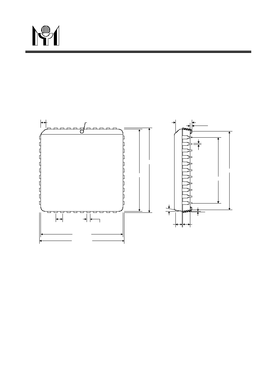
13.0 PACKAGE DIMENSION
44 PIN PLCC
Unit: Inch
PIN #1 HOLE
0.653 +/-0.003
0.690 +/-0.005
0.6902 +/-0.005
0.653 +/-0.003
0.045*45
0
0.180 MAX.
0.020 MIN.
0.610 +/-0.02
0.500
0.070
0.070
7
0
TYP.
0.010
0.050 TYP.
0.013~0.021 TYP.
0.026~0.032 TYP.