 | –≠–ª–µ–∫—Ç—Ä–æ–Ω–Ω—ã–π –∫–æ–º–ø–æ–Ω–µ–Ω—Ç: MTD971 | –°–∫–∞—á–∞—Ç—å:  PDF PDF  ZIP ZIP |
MYSON
TECHNOLOGY
MTD971
(Preliminary)
100BaseTX PMD
This datasheet contains new product information. Myson Technology reserves the rights to modify the product specification
without notice. No liability is assumed as a result of the use of this product. No rights under any patent accompany the sale of the
product.
MTD971 Revision 2.52 03/05/1997
1/9
FEATURES
∑
Complies with X3T12 FDD over copper (TP-PMD) standards.
∑
Complies with IEEE 802.3 Fast Ethernet 100Base-TX standards.
∑
Integrated UTP receiver with adaptive equalization for CAT-5 cable.
∑
Intelligent squelching for signal detection status and LED output.
∑
ECL level NRZI to MLT-3 level signal coding and decoding.
∑
Integrated UTP transmitter with current mode output.
∑
Transmitter enabler control for a high impedance state.
∑
External loopback control for diagnostics.
∑
Minimum external component connections for sharing termination and magnetics with most 10-
BaseT transceivers.
∑
28-pin PLCC packages.
GENERAL DESCRIPTION
MTD971 integrates all necessary functions for TP-PMD standards and is specifically designed for
100BaseTX Fast Ethernet transceiver applications. The receiving function includes built-in adaptive
equalization and DC wandering compensation circuits for Category-5 UTP cable, MLT-3 to NRZI
decoding circuits, and ECL level output buffer. The transmission function includes an ECL input buffer,
an NRZI to MLT-3 converter, and a differential current output amplifier.
MTD971 provides an easy media interface with most 10BaseT transceivers or 100Base PHY/PMA
devices, such as MTD972. In general, by sharing a common termination network and magnetics with the
10BaseT media interface, a minimum external component count and low EMI can be achieved.
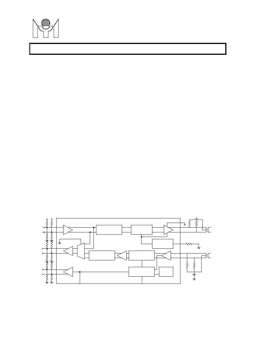
BLOCK DIAGRAM
+
-
+
-
+
-
MUX
MLT-3 TO NRZI
ENCODER
NRZI TO MLT-3
ENCODER
+
-
EQUALIZATION
FILTER
WAVEFORM
SHAPING
gm
+
-
+
-
TRANSMIT
REFERENCE
RECEIVE
REF
ADAPTIVE
CONTROL
XOEN
TXOP
TXON
XREF
TPIP
TPIN
EQSL
SDSTN
SDOP
SDON
RXOP
RXON
TXIP
TXIN
LBKN
R3
160
R1
160
R2
260
R4
260
R7
160
R5
160
R6
260
R8
260
R7
160
R5
160
R6
260
R8
260
RT1
50
RT2
50
2K
RXREF
RT4
50
RT3
50
1:1CT
1:1CT
CCM
0.1u
PHY/PMA INTERFACE
MEDIA INTERFACE
MYSON
TECHNOLOGY
MTD971
(Preliminary)
MTD971 Revision 2.52 03/05/1997
2/9
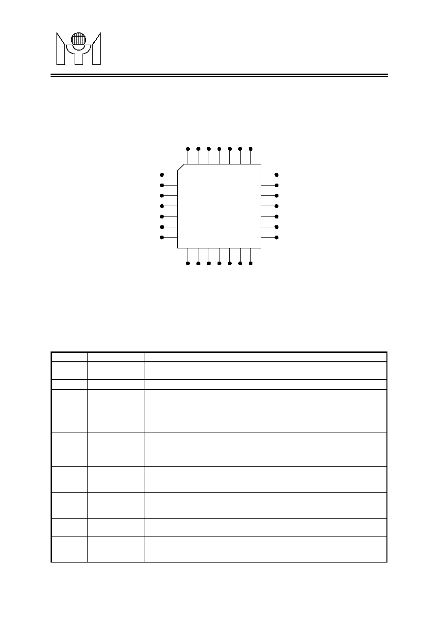
1.0 CONNECTION DIAGRAM
28-pin PLCC
MTD971
VCCR1
GNDR1
TPIP
TPIN
GNDR2
VCCR2
N.C.
RXOP
RXON
VCCE
GNDE
SDON
SDOP
LBKN
SDSTN
VCCX3
GNDX3
TXIP
TXIN
EQSL
XOEN
VCCX1
XREF
GNDX1
TXON
TXOP
GNDX2
VCCX2
1
22
15
8
2.0 PIN DESCRIPTIONS
Name
Pin#
I/O
Description
TPIP,
TPIN
2,1
I
UTP Differential Receiving Inputs. These differential inputs connect to
the UTP media through an isolation transformer for data reception.
N.C.
26
N.C.
TXOP,
TXON
9,8
O
UTP Differential Transmission Outputs. These differential outputs
connect to the UTP media through an isolation transformer for data
transmission. The output provides a differential current sink and should be
biased by two 50 Ohm external termination resistors from TXOP and TXON
to +5V.
XREF
6
I
Transmission Reference. An external precision resistor connected
between XREF and 0V provides the current reference for the transmission
output current. Typically a 2.0KOhm 1% resistor that yields a +/- 40 mA
differential current output on TXOP and TXON should be used.
XOEN
18
I
Transmission Output Enabler. A TTL level input that should be low for
normal transmission functions. When XOEN is high, the transmission
output is put in high impedance mode.
TXIP,
TXIN
15,16
I
Transmission Differential Data Inputs. ECL level inputs that receive
NRZI data from PHY/PMA and convert it into MLT-3 format for
transmission.
RXOP,
RXON
25,24
O
Receiving Differential Data Outputs. ECL level outputs that receive data
in NRZI format.
SDOP
SDON
20,21
O
Signal Detection Differential Outputs. ECL level outputs as the signal
detection status from the UTP media. The presence of signal detection is
determined by comparing the received media energy with an internal fixed

MYSON
TECHNOLOGY
MTD971
(Preliminary)
MTD971 Revision 2.52 03/05/1997
3/9
threshold.
SDSTN
12
O
Signal Detection Status. An open-collector output for signal detection
status. When presence of signal detection is determined, this output is
pulled low. This can be used to drive an LED status indicator or connected
directly to a PHY/PMA device.
EQSL
17
I
Equalization Selection. This is a 3-level CMOS input for determining the
level of equalization. When EQSL is pulled up above 4.2 V, no receiving
equalization is performed on a received signal. When EQSL is pulled down
below 0.8V, full equalization is performed on a received signal. The
adaptive equalization is selected when this pin is left floating.
LBKN
19
I
Loopback Enabler. This is a TTL level input which controls the loopback
function for diagnostic purposes. LBKN should be low for normal operation.
When LBKN is high, MTD971 is in loopback mode. In this mode, the
transmission data presented on TXIP and TXIN is directly routed back to
RXOP and RXON. SDOP and SDON are forced to assume an asserted
state in loopback mode.
VCC
4,5,11,13,
23, 27
P
+5V power supply.
GND
3,7,10,14,
22, 28
P
0V power supply.
3.0 FUNCTIONAL DESCRIPTIONS
MTD971 is an integrated TP-PMD transceiver compliant with 100BaseTX Fast Ethernet standards,
which allows a 125Mbaud/100Mbs data rate with length up to 100m over Category 5 unshielded twisted
cable.
Transmission Path
The transmission path receives transmitted data from PHY through TXIP/TXIN differential ECL pins.
The data from PHY in NRZI format is converted to MLT-3 format by extracting the data edges in the data
stream. To minimize EMI, a waveform shaping circuit is used to control the edge rate of the output
waveform. An output buffer in transconductance amplifier form is used to provide the differential current
output on TXOP and TXON pins.
Because the output is a differential current sink source, external load resistors of 50 Ohm should be
connected from TXOP/TXON to the +5V supply.
These 2 resistors also set the source termination resistor value to 100 Ohm for driving the UTP cable
under 1:1 isolation transformer. The center-tap of the transformer should also be connected to +5V in
order to prevent the droop of output level and common mode transient in the data stream.
The transmission output current level is determined by an internal reference circuit and an external
precision resistor. For 100BaseTX, a 2K Ohm precision resistor should be connected between the
XREF pin and 0V. This provides for a differential transmission current of 40 mA or 2V p-p on the
differential transmission output when properly terminated.
For MTD971 implementation of MLT-3 format, the mid-level is generated by sinking equal amounts of
current on TXOP and TXON pins. Thus, the transmission output buffer is always active during normal
operation. The current drain in the idle state may thus interfere with other circuits sharing the termination
resistors and isolation transformer. To complete the shutting off of the transmission output buffer, set
XOEN to high. This will put the transmission output TXOP and TXON in the high impedance state.
XOEN should be low for normal 100 Mbps operation. XOEN is typically controlled by the PHY device,
which selects the operation speed of the transceiver. Because MTD971 provides the output in the
current source mode and can be put into a high impedance state, it can be easily connected with a
10BaseT transceiver with a current source output by sharing the same load resistors and isolation

MYSON
TECHNOLOGY
MTD971
(Preliminary)
MTD971 Revision 2.52 03/05/1997
4/9
magnetics.
MYSON
TECHNOLOGY
MTD971
(Preliminary)
MTD971 Revision 2.52 03/05/1997
5/9
Receiving Path
The signal received from the UTP cable is coupled to the TPIP and TPIN pins differentially through a 1:1
isolation transformer. To provide proper termination for the cable, two 50 Ohm resistors should be used
across TPIP and TPIN with the center connection connected to a 0.1u capacitor.
The received differential signal is first buffered by an amplifier. An equalization filter is used to
compensate for the cable loss. The amplifier also outputs to an adaptive control circuit, which compares
the received signal with an internal reference to determine the cable length and set the level of
equalization accordingly. The level of equalization can be optionally forced by the EQSL pin. Forcing
EQSL low/high will turn the equalization fully on/off, respectively. Allowing EQSL to float will allow
equalization in the adaptive mode.
Signal detection status is determined by the adaptive control circuit. A built-in hysteresis is implemented
in the signal detection circuits. The signal detection status is asserted when a received signal exceeds
750 mV p-p and is deserted when it is below 250 mV p-p. An open-drain output, SDSTN, is provided for
driving an LED display. It can also be used to connect to the PHY/PMA device directly. Differential ECL
level outputs, SDOP and SDON, are also implemented for interfacing with PHY/PMA.
The differential signal after equalization is then sliced and fed into MLT-3 to the NRZI converter. The
conversion occurs by adding the complementary signals with respect to the mid-point of the signal swing.
A multiplexer is used between the received NRZI data and the output ECL buffer. The multiplexer is
controlled by the loopback enabler pin, LBKN. When LBKN is high, loopback is enabled, then the data on
TXIP and TXIN is directly routed back to RXOP and RXON for diagnostic purposes. Signal detection
status is also asserted in the loopback mode. LBKN should be low for normal operations.
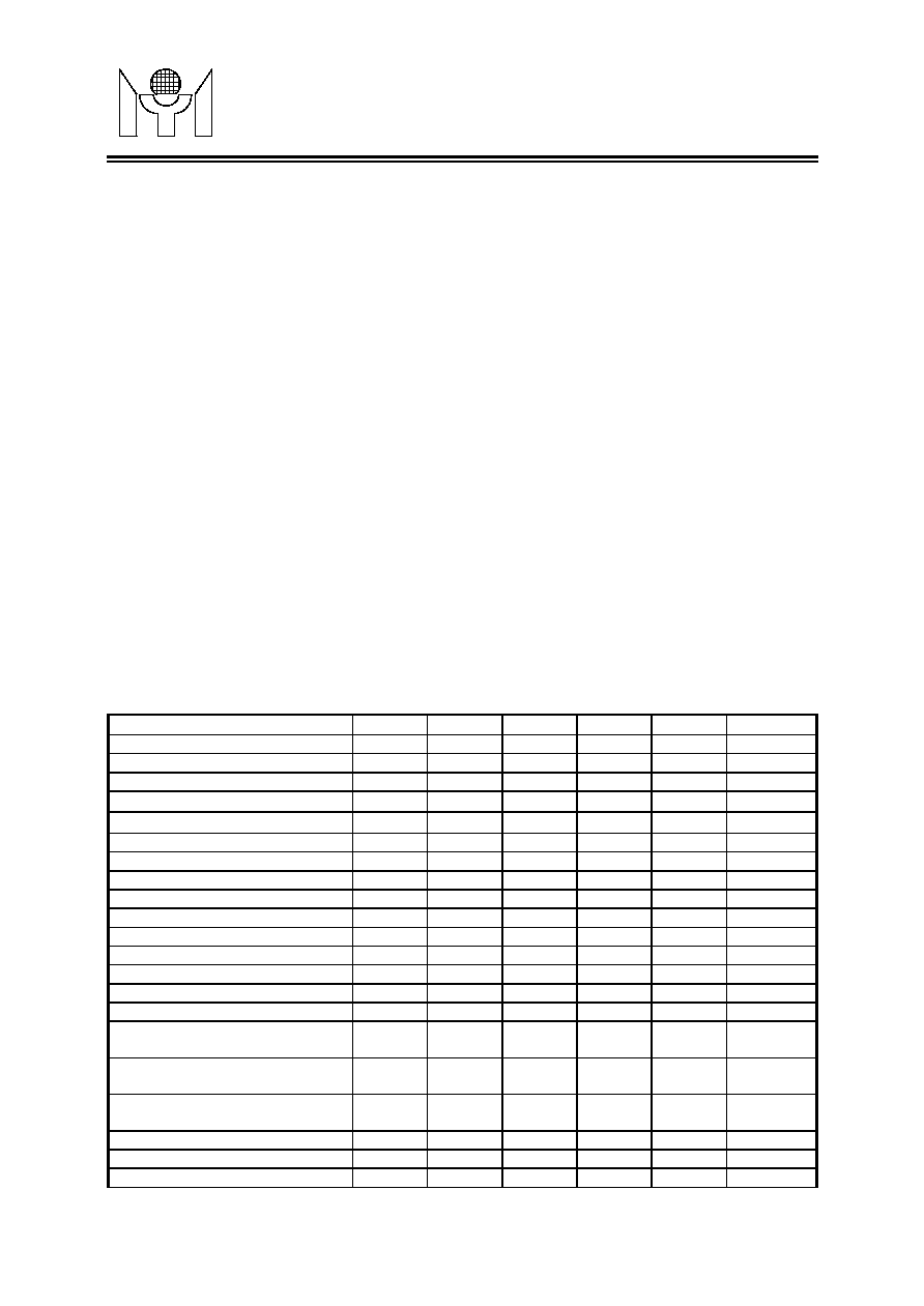
4.0 ELECTRONIC CHARACTERISTICS
DC Characteristics
Parameter
Symbol
Min
Typ
Max
Unit
Note
Supply Current, internal
Icc1
-
70
85
mA
1
Supply Current, transmission
Icc2
-
110
125
mA
2
Supply Current, all
Icc3
-
165
180
mA
3
TTL Input High Level for LBKN
VIH,T
2.2
-
-
V
TTL Input Low Level for LBKN
VIL,T
-
-
0.8
V
Output Low Level for SDSTN
VOL,T
-
-
0.8
V
(IOL=4mA)
CMOS Input High Level for EQSL
VIH,C
4.0
-
-
V
CMOS Input Float Level for EQSL
VIF,C
1.5
2.5
3.5
V
CMOS Input Low Level for EQSL
VIL,C
-
-
1.0
V
Input Leakage Current for EQSL
IIL
-0.5
-
0.5
mA
ECL Common Mode Input Level
VIC,E
2.2
-
Vcc
V
4
ECL Differential Input Level
VID,E
0.4
-
1.5
V
4
ECL Common Mode Input Current
IIC,E
-
25
50
uA
4
ELC Output High Level
VOH,E
-1.025
-
-0.880
V
5
ECL Output Low Level
VOL,E
-1.810
-
-1.620
V
5
Transmission Output Current
Differential
IXMT
38
40
42
mA
6
Transmission Output Current
Mismatch
IXMT,M
-0.8
0
0.8
mA
6
Transmission Output Current
Offset
IXMT,O
-0.5
0
0.5
mA
7
Receiving Common Mode Range
VIC,R
2.2
3.2
4.2
V
8
Receiving Input Bias Current
IIB,R
-
10
20
uA
8
Receiving Differential Input Level
VID,R
-
-
1.5
V
8