MTP805 / MTP805A / MTP805M
8051 Embedded USB/PS2 Keyboard/Mouse Controller
sales@myson.com.tw
www.myson.com.tw
Rev. 1.2 December 2002
page 1 of 21
Myson Century, Inc.
Taiwan:
No. 2, Industry East Rd. III,
Science-Based Industrial Park, Hsin-Chu, Taiwan
Tel: 886-3-5784866 Fax: 886-3-5784349
USA:
4020 Moorpark Avenue Suite 115
San Jose, CA, 95117
Tel: 408-243-8388 Fax: 408-243-3188
GENERAL DESCRIPTION
The MTP805/MTP805A/MTP805M micro-controller is
an 8051 CPU core embedded device specially
tailored to USB/PS2 Keyboard/Mouse applications. It
includes an 8051 CPU core, 256-byte SRAM, Low
Speed USB Interface and an 8K-byte internal
program Flash-ROM.
FEATURES
∑ 8051 core, 6MHz operating frequency.
∑ 256-byte RAM, 8K-byte program Flash-ROM
(MTP805M) or 8K-byte program Mask-ROM
(MTP805, MTP805A).
∑ Compliant with Low Speed USB Spec.1.1
including 3 Endpoints: one is Control endpoint (8-
byte IN & 8-byte OUT FIFOs), the other two are
Interrupt endpoints (8-byte IN FIFOs).
∑ Built-in 5V-to-3.3V regulator for USB Interface.
∑ Suspend / Resume operation.
∑ Idle and Power down mode wake-up by interrupt.
∑ 8 dedicated Key scan input pins and 18/19 Key
scan output pins.
∑ Built-in low power reset circuit and Watchdog timer.
∑ PS2 compatible mouse interface.
∑ PS2 compatible keyboard interface share with
USB interface.
∑ CPU clock can be double by S/W setting.
∑ I/O pads tolerate to 5V voltage.
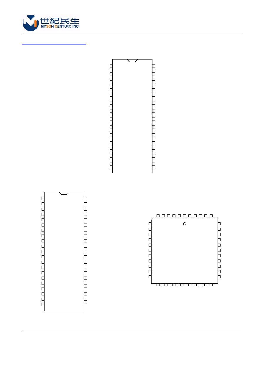
∑ Available in die form, 40-pin PDIP, 42-pin SDIP or
44-pin PLCC package.
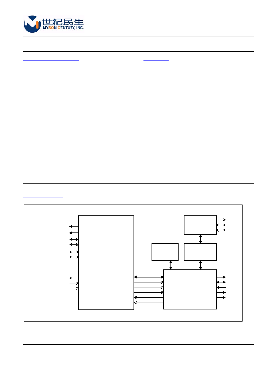
BLOCK DIAGRAM
P1.0~7
8051
KSO0~7
P2.0~7
KSO8~15
P3.0
MSDATA
P3.1
MSCLK
P3.4
PS2CLK
P3.5
PS2DATA
OSC2
OSC1
RESET
DBUS
P0.0~7
/RD
/WR
ALE
/INT0
/INT1
P3.7
P3.6
ALE
P3.2
P3.3
XFR
SIE
XCVR
KSO16~17
GPIO0~1
KSI0~7
LED0~2
GPO0
V33
DP
DM
WDT
MTP805 / MTP805A / MTP805M
page 2 of 21
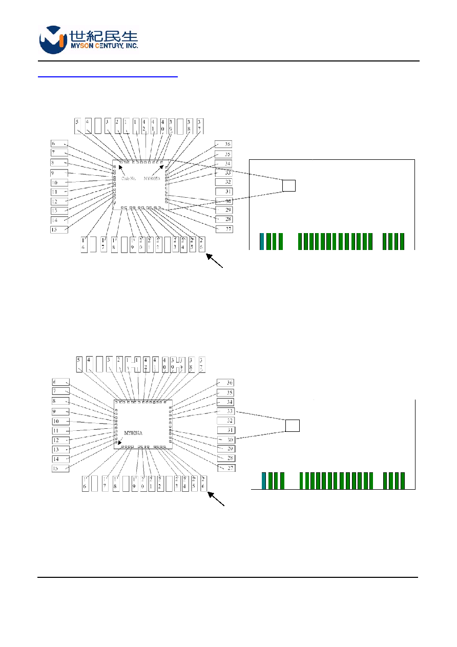
PIN CONNECTION (TOP VIEW)
MTP805S/
MTP805AS/
MTP805MS
42-Pin
SDIP
40
1
39
38
37
36
35
34
33
32
31
30
29
28
27
26
25
24
23
22
21
2
3
4
5
6
7
8
9
10
11
12
13
14
15
16
17
18
19
20
DM/PS2DATA
V33
DP/PS2CLK
VDD
LED1
LED2
LED0
GPO0/LED3
MSDATA
GPIO1
MSCLK
KSO10
KSO16
KSO9
KSO15
KSO13
KSO12
KSO14
KSO11
42
41
KSO17
GPIO0
MTP805V/
MTP805AV/
MTP805MV
44-Pin
PLCC
7
8
9
10
11
12
13
14
15
16
17
39
38
37
36
35
34
33
32
31
30
29
KSO
10
24
KSO
11
KSO
12
KSO
9
KSO
13
KSO
14
NC
KSO
5
KSO
6
KSO
7
KSO
8
23
22
21
20
28
27
26
25
KSI1
6
5
4
3
2
1
44
43
42
41
40
KSI0
RST
OS
C2
OS
C1
VSS
DP/PS2CLK
DM/PS2DAT
A
V33
VDD
NC
19
18
KSI2
KSI3
KSI5
KSI6
KSI7
KSO0
KSO1
KSO2
KSO3
KSO4
KSI4
KSO16
KSO15
KSO17
GPIO0
LED0
LED1
LED2
MSCLK
MSDATA
GPO0/LED3
GPIO1
VSS
OSC1
OSC2
RST
KSI0
KSI1
KSI2
KSI3
KSI4
KSI5
KSI6
KSI7
KSO0
KSO1
KSO2
KSO3
KSO4
KSO5
KSO6
KSO7
KSO8
MTP805N/
MTP805AN/
MTP805MN
40-Pin
PDIP
40
1
39
38
37
36
35
34
33
32
31
30
29
28
27
26
25
24
23
22
21
2
3
4
5
6
7
8
9
10
11
12
13
14
15
16
17
18
19
20
VSS
OSC1
OSC2
RST
KSI0
KSI1
KSI2
KSI3
KSI4
KSI5
KSI6
KSI7
KSO0
KSO1
KSO2
KSO3
KSO4
KSO5
KSO6
KSO7
DM/PS2DATA
V33
DP/PS2CLK
VDD
LED1
LED2
LED0
GPO0/LED3
MSDATA
KSO17
MSCLK
KSO16
KSO14
KSO13
KSO15
KSO12
KSO10
KSO9
KSO11
KSO8
MTP805 / MTP805A / MTP805M
page 5 of 21
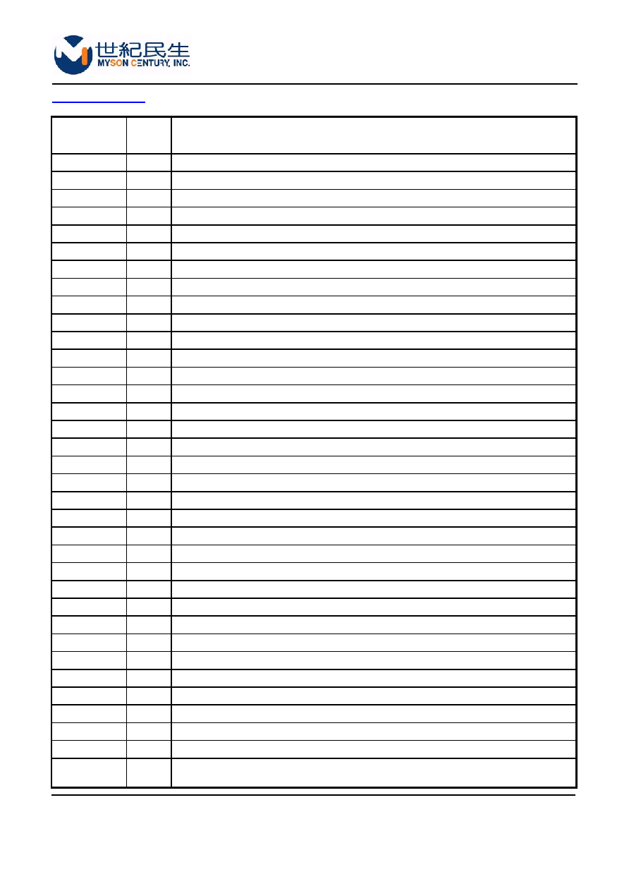
PIN DESCRIPTION
Name Type
Description
VSS -
Ground.
OSC1 I
Oscillator
input.
OSC2 O
Oscillator
output.
RST
I
Active high reset. (with internal pull-down resistor)
KSI0
I
Key scan input 0. (Schmitt-trigger with 10K/33K/50K pull-up resistor)
KSI1
I
Key scan input 1. (Schmitt-trigger with 10K/33K/50K pull-up resistor)
KSI2
I
Key scan input 2. (Schmitt-trigger with 10K/33K/50K pull-up resistor)
KSI3
I
Key scan input 3. (Schmitt-trigger with 10K/33K/50K pull-up resistor)
KSI4
I
Key scan input 4. (Schmitt-trigger with 10K/33K/50K pull-up resistor)
KSI5
I
Key scan input 5. (Schmitt-trigger with 10K/33K/50K pull-up resistor)
KSI6
I
Key scan input 6. (Schmitt-trigger with 10K/33K/50K pull-up resistor)
KSI7
I
Key scan input 7. (Schmitt-trigger with 10K/33K/50K pull-up resistor)
KSO0
O
Key scan output 0 (8051's P1.0). (Pseudo open-drain)
KSO1
O
Key scan output 1 (8051's P1.1). (Pseudo open-drain)
KSO2
O
Key scan output 2 (8051's P1.2). (Pseudo open-drain)
KSO3
O
Key scan output 3 (8051's P1.3). (Pseudo open-drain)
KSO4
O
Key scan output 4 (8051's P1.4). (Pseudo open-drain)
KSO5
O
Key scan output 5 (8051's P1.5). (Pseudo open-drain)
KSO6
O
Key scan output 6 (8051's P1.6). (Pseudo open-drain)
KSO7
O
Key scan output 7 (8051's P1.7). (Pseudo open-drain)
KSO8
O
Key scan output 8 (8051's P2.0). (Pseudo open-drain)
KSO9
O
Key scan output 9 (8051's P2.1). (Pseudo open-drain)
KSO10
O
Key scan output 10 (8051's P2.2). (Pseudo open-drain)
KSO11
O
Key scan output 11 (8051's P2.3). (Pseudo open-drain)
KSO12
O
Key scan output 12 (8051's P2.4). (Pseudo open-drain)
KSO13
O
Key scan output 13 (8051's P2.5). (Pseudo open-drain)
KSO14
O
Key scan output 14 (8051's P2.6). (Pseudo open-drain)
KSO15
O
Key scan output 15 (8051's P2.7). (Pseudo open-drain)
KSO16
I/O
Key scan output 16. (Pseudo open-drain)
KSO17
I/O
Key scan output 17. (Pseudo open-drain)
GPIO0
I/O
General purpose I/O 0. (Pseudo open-drain)
GPIO1
I/O
General purpose I/O 1. (Pseudo open-drain)
MSDATA
I/O
Mouse data (8051's P3.0). (Pseudo open-drain)
MSCLK
I/O
Mouse clock (8051's P3.1). (Pseudo open-drain)
GPO0/LED3
O
General purpose output 0; or output pin to drive LED3.
(Open-drain with 420 ohm serial resistor)