 | ÐлекÑÑоннÑй компоненÑ: MTV212M | СкаÑаÑÑ:  PDF PDF  ZIP ZIP |
þÿ
MTV212M64
8051 Embedded Monitor Controller MTP Type
sales@myson.com.tw
www.myson.com.tw
Rev. 1.3 August 2002
page 1 of 27
Myson Century, Inc.
Taiwan:
No. 2, Industry East Rd. III,
Science-Based Industrial Park, Hsin-Chu, Taiwan
Tel: 886-3-5784866 Fax: 886-3-5784349
USA:
4020 Moorpark Avenue Suite 115
San Jose, CA, 95117
Tel: 408-243-8388 Fax: 408-243-3188
FEATURES
·
8051 core, 12MHz operating frequency.
·
1024-byte RAM, 64K-byte program Flash-ROM.
·
·
Maximum 14 channels of 9V open-drain PWM DAC.
·
Maximum 32 bi-directional I/O pins.
·
SYNC processor for composite separation/insertion, H/V polarity/frequency check, polarity adjustment and
programmable clamp pulse output.
·
Built-in self-test pattern generator with three free-running timings.
·
Built-in low power reset circuit.
·
Compliant with VESA DDC1/2B/2Bi/2B+ standard.
·
Dual slave IIC addresses.
·
Single master IIC interface for internal device communication.
·
4-channel 6-bit ADC.
·
Watchdog timer with programmable interval.
·
Compliant with Low Speed USB Spec.1.1 including 2 Endpoints: one is Control endpoint (8-byte IN & 8-byte
OUT FIFOs), the other one is Interrupt endpoint (8-byte IN FIFO).
·
Built-in 3.3V regulator for USB Interface.
·
40-pin DIP, 42-pin SDIP or 44-pin PLCC package.
GENERAL DESCRIPTIONS
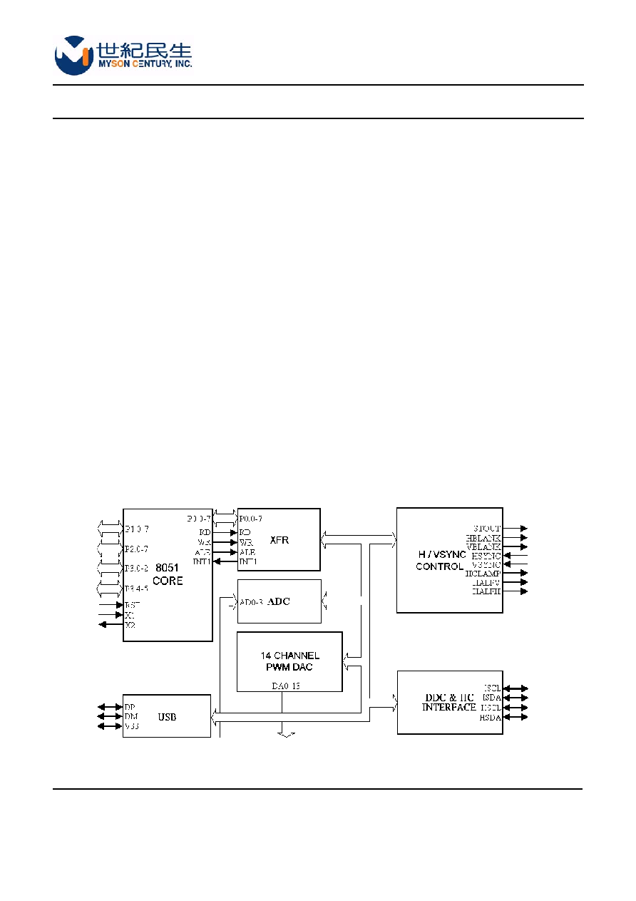
The MTV212M micro-controller is an 8051 CPU core embedded device specially tailored to Monitor
applications. It includes an 8051 CPU core, 1024-byte SRAM, SYNC processor, 14 built-in PWM DACs, VESA
DDC interface, 4-channel A/D converter, Low Speed USB Interface and a 64K-byte internal program Flash-
ROM.
BLOCK DIAGRAM
MTV212M64
Page 2 of 27
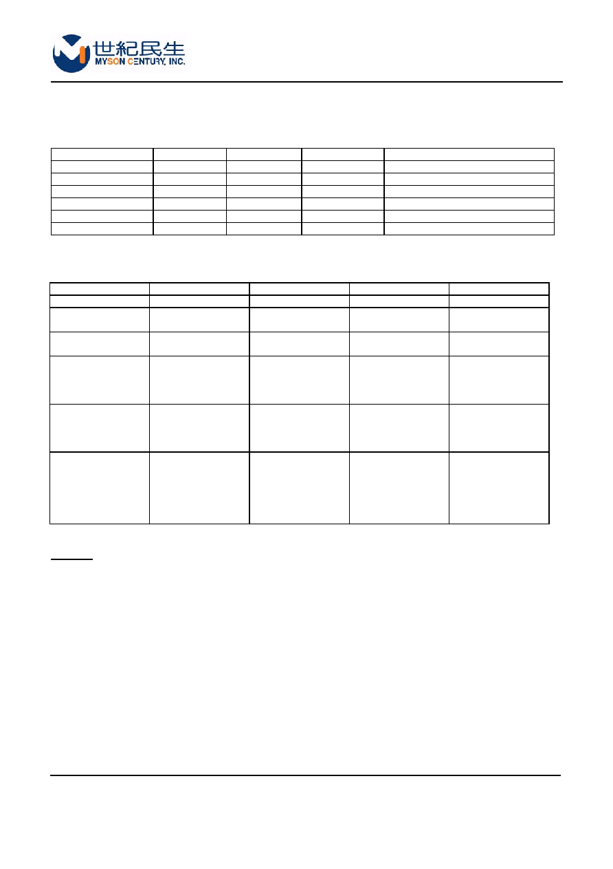
DEVICE SUMMARY
The MTV212M is the MTP (Multi-Time Programming) type device for all of MTV212A mask ROM derivatives,
the memory size and package differences please see the table below:
Part Number
USB
ROM
RAM
Package
MTV212A16
No
16K
256
PDIP40, SDIP42, PLCC44
MTV212A24
No
24K
512
PDIP40, SDIP42, PLCC44
MTV212A32
No
32K
512
PDIP40, SDIP42, PLCC44
MTV212A32U
Yes
32K
768
PDIP40, SDIP42, PLCC44
MTV212A48U
Yes
48K
768
PDIP40, SDIP42, PLCC44
MTV212A64U
Yes
64K
1024
PDIP40, SDIP42, PLCC44
The use of Auxiliary RAM (AUXRAM) is limited for targeted mask ROM, the allowable XBANK (35h) bank
selection is defined as the table below:
Part Number
RAM
Xbnk2 Xbnk1 Xbnk0
MTV212A16
256
- - -
MTV212A24
512 0 0 0
0 0 1
MTV212A32
512 0 0 0
0 0 1
MTV212A32U
768 0 0 0
0 0 1
0 1 0
0 1 1
MTV212A48U
768 0 0 0
0 0 1
0 1 0
0 1 1
MTV212A64U
1024
0 0 0
0 0 1
0 1 0
0 1 1
1 0 0
1 0 1
Remark:
The major pin connection differences between USB (MTV212M64U) and non-USB (MTV212M64) types are
pin# 4, #5 and #6 for SDIP42 and PLCC44. The pin name of USB device is V33CAP(#4), VM(#5) and VP(#6),
while NC (No Connection) for non-USB device.
PIN CONNECTION
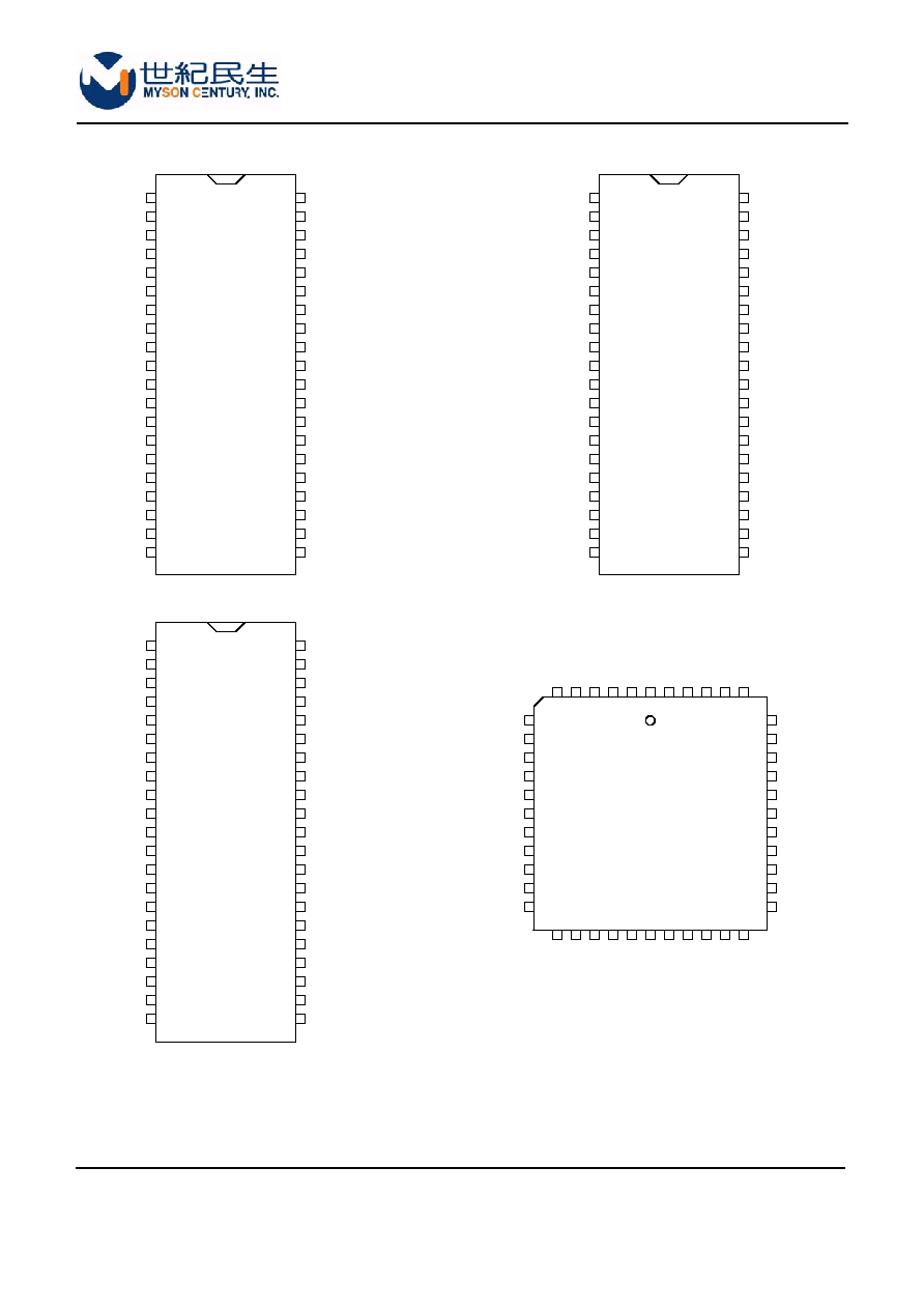
MTV212M64
Page 3 of 27
MTV212M
40 Pin
PDIP #1
Non-USB
DA2/P5.2
40
1
39
38
37
36
35
34
33
32
31
30
29
28
27
26
25
24
23
22
21
2
3
4
5
6
7
8
9
10
11
12
13
14
15
16
17
18
19
20
DA1/P5.1
DA0/P5.0
RST
VDD
VSS
X2
X1
ISDA/P3.4/T0
ISCL/P3.5/T1
STOUT/P4.2
P2.2/AD2
P1.0
P1.1
P3.2/INT0
P1.2
P1.3
P1.4
P1.5
P1.6
HSYNC
DA3/P5.3
VSYNC
DA4/P5.4
DA8/HALFH
DA9/HALFV
DA5/P5.5
HBLANK/P4.1
DA7/HCLAMP
DA6/P5.6
VBLANK/P4.0
P2.7/DA13
P2.5/DA11
P2.4/DA10
P2.6/DA12
HSCL/P3.0/Rxd
P2.0/AD0
P2.1/AD1
HSDA/P3.1/Txd
P1.7
MTV212M
40 Pin
PDIP #2
USB
DA2/P5.2
40
1
39
38
37
36
35
34
33
32
31
30
29
28
27
26
25
24
23
22
21
2
3
4
5
6
7
8
9
10
11
12
13
14
15
16
17
18
19
20
DA1/P5.1
DA0/P5.0
RST
VDD
VSS
X2
X1
ISDA/P3.4/T0
ISCL/P3.5/T1
STOUT/P4.2
P2.2/AD2
P1.0
P1.1
P3.2/INT0
P1.2
P1.3
V33CAP
DM
DP
HSYNC
DA3/P5.3
VSYNC
DA4/P5.4
DA8/HALFH
DA9/HALFV
DA5/P5.5
HBLANK/P4.1
DA7/HCLAMP
DA6/P5.6
VBLANK/P4.0
P1.6
P1.4
P2.4/DA10
P1.5
HSCL/P3.0/Rxd
P2.0/AD0
P2.1/AD1
HSDA/P3.1/Txd
P1.7
MTV212M
42 Pin
SDIP
USB
or
Non-USB
DA2/P5.2
40
1
39
38
37
36
35
34
33
32
31
30
29
28
27
26
25
24
23
22
21
2
3
4
5
6
7
8
9
10
11
12
13
14
15
16
17
18
19
20
DA1/P5.1
DA0/P5.0
RST
VDD
VSS
X2
X1
ISDA/P3.4/T0
ISCL/P3.5/T1
STOUT/P4.2
P2.2/AD2
P1.0
P1.1
P3.2/INT0
P1.2
P1.3
V33CAP/NC
DM/NC
DP/NC
HSYNC
DA3/P5.3
VSYNC
DA4/P5.4
DA8/HALFH
DA9/HALFV
DA5/P5.5
HBLANK/P4.1
DA7/HCLAMP
DA6/P5.6
VBLANK/P4.0
P1.6
P2.4/DA10
P1.5
HSCL/P3.0/Rxd
P2.0/AD0
P2.1/AD1
HSDA/P3.1/Txd
P1.7
42
41
P2.5/DA11
P2.6/DA12
P1.4
MTV212M
44 Pin
PLCC
USB
or
Non-USB
7
8
9
10
11
12
13
14
15
16
17
39
38
37
36
35
34
33
32
31
30
29
P1.6
24
P1.7
P2.1/AD1
P1.5
P2.0/AD0
HSDA/P3.1/Txd
P1.1
P3.2/INT0
P1.2
P1.3
P1.4
23
22
21
20
28
27
26
25
DP/NC
6
5
4
3
2
1
44
43
42
41
40
DM/NC
V33CAP/NC
DA0/P5.0
DA1/P5.1
DA2/P5.2
VSYNC
HSYNC
DA3/P5.3
DA4/P5.4
DA5/P5.5
19
18
RST
VDD
VSS
X2
X1
ISDA/P3.4/T0
ISCL/P3.5/T1
STOUT/P4.2
P2.2/AD2
P1.0
P2.3/AD3
P2.4/DA10
HSCL/P3.0/Rxd
P2.5/DA11
P2.6/DA12
DA8/HALFH
DA9/HALFV
HBLANK/P4.1
DA7/HCLAMP
DA6/P5.6
VBLANK/P4.0
P2.7/DA13
MTV212M64
Page 4 of 27
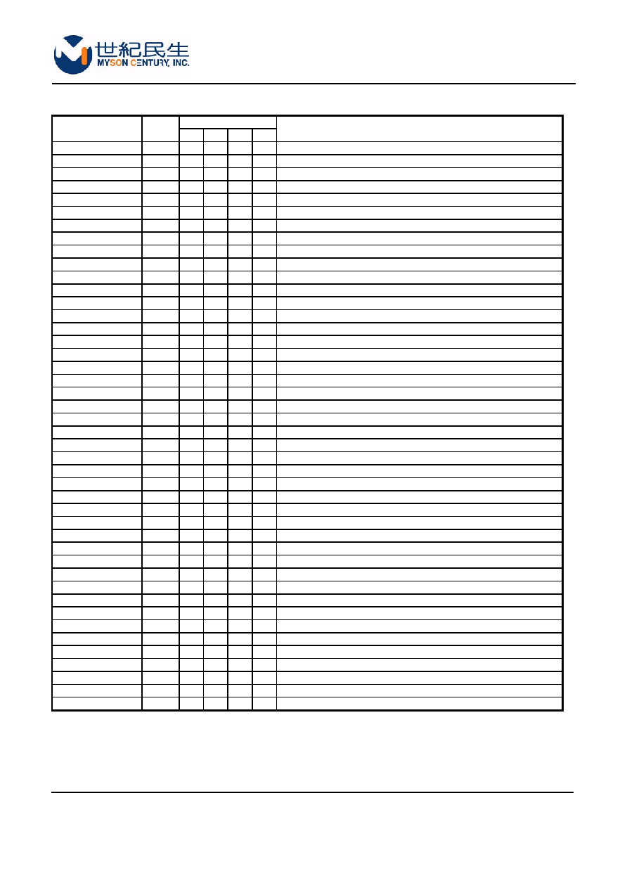
PIN DESCRIPTION
Pin#
Name Type
40 40 42 44
Description
DA2/P5.2
I/O
1
1
1
1
PWM DAC output / General purpose I/O (open drain).
DA1/P5.1
I/O
2
2
2
2
PWM DAC output / General purpose I/O (open drain).
DA0/P5.0
I/O
3
3
3
3
PWM DAC output / General purpose I/O (open drain).
V33CAP/NC
I/O
-
4
4
4
3.3V Regulator Capacitor connection or NC.
DM/NC
I/O - 5 5 5
USB
DM
or
NC.
DP/NC
I/O
-
6
6
6
USB DP or NC.
RST
I 4 7 7 7
Active
high
reset.
VDD
- 5 8 8 8
Positive
Power
Supply.
P2.3/AD3
I/O
-
-
-
9
General purpose I/O / ADC Input.
VSS
- 6 9 9 10 Ground.
X2
O 7 10 10 11 Oscillator
output.
X1
I
8 11 11 12 Oscillator
input.
ISDA/P3.4/T0
I/O
9
12 12 13 Master IIC data / General purpose I/O / T0.
ISCL/P3.5/T1
I/O
10 13 13 14 Master IIC clock / General purpose I/O / T1.
STOUT/P4.2
O
11 14 14 15 Self-test video output / General purpose Output.
P2.2/AD2
I/O
12 15 15 16 General purpose I/O / ADC Input.
P1.0
I/O 13 16 16 17 General
purpose
I/O.
P1.1
I/O 14 17 17 18 General
purpose
I/O.
P3.2/INT0
I
15 18 18 19 General purpose Input / INT0.
P1.2
I/O 16 19 19 20 General
purpose
I/O.
P1.3
I/O 17 20 20 21 General
purpose
I/O.
P1.4
I/O 18 21 21 22 General
purpose
I/O.
P1.5
I/O 19 22 22 23 General
purpose
I/O.
P1.6
I/O 20 23 23 24 General
purpose
I/O.
P1.7
I/O 21 24 24 25 General
purpose
I/O.
P2.1/AD1
I/O
22 25 25 26 General purpose I/O / ADC Input.
P2.0/AD0
I/O
23 26 26 27 General purpose I/O / ADC Input.
HSDA/P3.1/Txd
I/O
24 27 27 28 Slave IIC data / General purpose I/O / Txd.
HSCL/P3.0/Rxd
I/O
25 28 28 29 Slave IIC clock / General purpose I/O / Rxd.
P2.4/DA10
I/O
26 29 29 30 General purpose I/O / PWM DAC output (open drain).
P2.5/DA11
I/O
27
-
30 31 General purpose I/O / PWM DAC output (open drain).
P2.6/DA12
I/O
28
-
31 32 General purpose I/O / PWM DAC output (open drain).
P2.7/DA13
I/O
29
-
-
33 General purpose I/O / PWM DAC output (open drain).
DA6/P5.6
I/O
30 30 32 34 PWM DAC output / General purpose I/O (open drain).
DA7/HCLAMP
O
31 31 33 35 PWM DAC output / Hsync clamp pulse output (open drain).
VBLANK/P4.0
O
32 32 34 36 Vertical blank / General purpose Output.
HBLANK/P4.1
O
33 33 35 37 Horizontal blank / General purpose Output.
DA9/HALFV
O
34 34 36 38 PWM DAC output / Vsync half freq. output (open drain).
DA8/HALFH
O
35 35 37 39 PWM DAC output / Hsync half freq. output (open drain).
DA5/P5.5
I/O
36 36 38 40 PWM DAC output / General purpose I/O (open drain).
DA4/P5.4
O
37 37 39 41 PWM DAC output / General purpose I/O (open drain).
DA3/P5.3
O
38 38 40 42 PWM DAC output / General purpose I/O (open drain).
HSYNC
I
39 39 41 43 Horizontal SYNC or Composite SYNC Input.
VSYNC
I 40 40 42 44 Vertical
SYNC
input.
MTV212M64
Page 5 of 27
FUNCTIONAL DESCRIPTIONS
1. 8051 CPU Core
MTV212M includes all 8051 functions with the following exceptions:
1.1 PSEN, ALE, RD and WR pins are disabled. The external RAM access is restricted to XFRs within the
MTV212M.
1.2 Port0, port3.3, port3.6 and port3.7 are not general-purpose I/O ports. They are dedicated to monitor special
application.
1.3 INT1 input pin is not provided, it is connected to special interrupt sources.
1.4 Port2 are shared with special function pins.
In addition, there are 2 timers, 5 interrupt sources and serial interface compatible with the standard 8051.
Note: All registers listed in this document reside in external RAM area (XFR). For internal RAM memory map
please refer to 8051 spec.
2. Memory Allocation
2.1 Internal Special Function Registers (SFR)
The SFR is a group of registers that are the same as standard 8051.
2.2 Internal RAM
There are total 256 bytes internal RAM in MTV212M, same as standard 8052.
2.3 External Special Function Registers (XFR)
The XFR is a group of registers allocated in the 8051 external RAM area 00h - 7Fh. Most of the registers are
used for monitor control or PWM DAC. Program can initialize Ri value and use "MOVX" instruction to access
these registers.
2.4 Auxiliary RAM (AUXRAM)
There are total 768 bytes auxiliary RAM allocated in the 8051 external RAM area 80h - FFh. The AUXRAM is
divided into six banks, selected by XBANK register. Program can initialize Ri value and use "MOVX" instruction
to access the AUXRAM.
00h
7Fh
80h
FFh
Internal RAM
Accessible by
indirect
addressing only
(Using
MOV A,@Ri
instruction)
Internal RAM
Accessible by
direct and indirect
addressing
SFR
Accessible by
direct addressing