Stock No. 23087-03 12/00
Subject to change without notice
1
EM033C08
NanoAmp Solutions, Inc.
1982 Zanker Road, San Jose, CA 95112
ph: 408-573-8878, FAX: 408-573-8877
www.nanoamp.com
EM033C08
Low Power 32Kx8 SRAM
Overview
The EM033C08 is an integrated memory device
containing a low power 256 Kbit Static Random
Access Memory organized as 32,768 words by 8
bits. The device is fabricated using an advanced
CMOS process and NanoAmp's high-speed/low-
power circuit technology. This device is designed
to be quite effective in battery powered products
with it's very low operating and standby currents. It
is also capable of full operation at voltages as low
as 1.5 volts. The device pinout is fully compatible
with NanoAmp's EM02R2XX family of Combination
RAM and ROM products making it very easy to
substitute an SRAM only device where the ROM is
unneccessary in the application. This device is
extremely stable over broad temperature and volt-
age ranges.
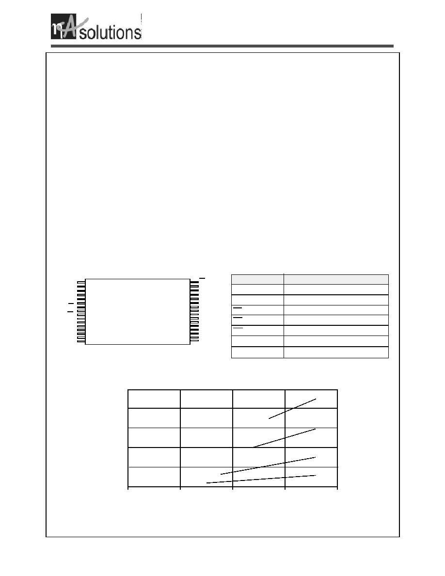
FIGURE 1: Pin Configuration
Features
�
Extended Operating Voltage Range
1.5 to 3.6 V
�
Very Low Standby Voltage
1.2 V
�
Extended Temperature Range
-20
o
to +80
o
C
�
Fast Cycle Time
100 ns (@ 2.7V)
�
Very Low Operating Current
I
CC
< 1 mA typical at 3V, 1 Mhz
�
Very Low Standby Current
I
SB
= 100 nA typical
�
Available in 32-pin STSOP package
TABLE 1: Pin Descriptions
EM033C08
STSOP
2
3
4
5
1
6
7
8
9
10
11
12
13
14
15
16
23
18
17
22
21
20
19
27
26
25
24
31
30
29
28
32
A11
A 9
A8
A13
WE
VCC
V S S
A14
A12
A7
A6
A5
A4
A2
A10
C E
VSS
A3
A1
A 0
D0
D1
D2
D3
D4
D5
D6
D7
OE
VCC
V S S
V S S
Pin Name
Pin Function
A0-A14
Address Inputs
D0-D7
Data Inputs/Outputs
CE
Chip Enable (Active Low)
OE
Output Enable (Active Low)
WE
Write Enable (Active Low)
V
CC
Power
V
SS
Ground
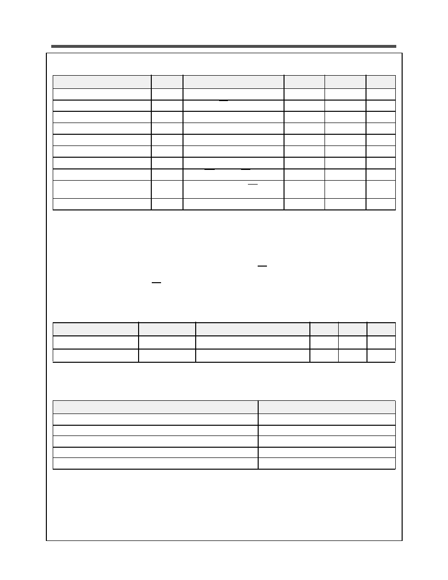
FIGURE 1: Operating Envelope
8
4
0
T
y
p
i
c
a
l
I
C
C
(
m
A
)
8 Mhz
2.5 Mhz
1 Mhz
V
CC
(V)
5 Mhz
6
2
0
1
2
3
4

Stock No. 23087-03 12/00
Subject to change without notice
2
EM033C08
NanoAmp Solutions, Inc.
FIGURE 2: Functional Block Diagram
FIGURE 3: Functional Description
*The device will consume active power in this mode whenever addresses are changed
TABLE 2: Absolute Maximum Ratings*
*Stresses greater than those listed above may cause permanent damage to the device. This is a stress rating only and
functional operation of the device at these or any other conditions above those indicated in the operating section of this
specification is not implied. Exposure to absolute maximum rating conditions for extended periods may affect reliability.
CE
WE
OE
D0-D7
MODE
POWER
H
X
X
High Z
Standby
Standby
L
H
H
High Z
Standby
Standby*
L
H
L
Data Out
READ
Active -> Standby*
L
L
X
Data In
WRITE
Active -> Standby*
Item
Symbol
Rating
Unit
Voltage on any pin relative to V
SS
V
IN,OUT
�0.3 to V
CC
+0.3
V
Voltage on V
CC
Supply Relative to V
SS
V
CC
�0.3 to 4.6
V
Power Dissipation
P
D
500
mW
Storage Temperature
T
STG
�40 to +125
o
C
Operating Temperature - Extended Commercial
T
A
-20 to +80
o
C
Control
Logic
32K x 8
RAM Array
Address
Decode
Logic
Address
Inputs
A
0
- A
14
CE
WE
OE
Input/
Output
Mux
and
Buffers
Data I/O
D0 - D7
Stock No. 23087-03 12/00
Subject to change without notice
3
EM033C08
NanoAmp Solutions, Inc.
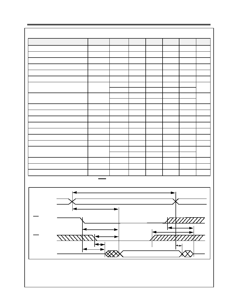
TABLE 3: Operating Characteristics (Over specified temperature range)
Notes:
Note 1. Operating current is a linear function of frequency and voltage. You may calculate operating current using the
formula shown with operating frequency (f) expressed in Mhz and operating voltage (V) in volts. Example: Operating
at 2 Mhz and 2.0 volts will draw a maximum current of 0.3*2*2 = 1.2 mA.
Note 2. This device assumes a standby mode whenever Chip Enable (CE) is disabled (high). It will also automatically
go into a standby mode whenever all input signals are quiescent (not toggling) whenever an access or write cycle is
completed regardless of the state CE. In order to achieve low standby current all input levels must be within 0.2 volts
of either V
CC
or GND.
TABLE 4: Capacitance*
Note: These parameters are verified in device characterization and are not 100% tested
TABLE 5: Timing Test Conditions
Item
Symbol
Test Conditions
Min.
Max.
Unit
Supply Voltage
V
CC
1.5
3.6
V
Data Retention Voltage
V
DR
CE = V
CC
1.2
3.6
V
Input High Voltage
V
IH
0.7V
CC
V
CC
+0.3
V
Input Low Voltage
V
IL
�0.3
0.3V
CC
V
Output High Voltage
V
OH
I
OH
= 200
�
A
V
CC
�0.2
V
Output Low Voltage
V
OL
I
OL
= �200
�
A
0.2
V
Input Leakage Current
I
LI
V
IN
= 0 to V
CC
1
�
A
Output Leakage Current
I
LO
OE = V
IH
or CE = 1
1
�
A
Operating Supply
Current (Note 1)
I
CC
V
IN
= V
CC
or 0V, CE = 0
0.3 * f * V
mA
Standby Current (Note 2)
I
SB
V
IN
= V
CC
or 0V
10
�
A
Item
Symbol
Test Condition
Min
Max
Unit
Input Capacitance
C
IN
V
IN
= 0V, f = 1 Mhz, T
A
= 25
o
C
5
pF
I/O Capacitance
C
I/O
V
IN
= 0V, f = 1 Mhz, T
A
= 25
o
C
5
pF
Item
Input Pulse Level
0.1V
CC
to 0.9 V
CC
Input Rise and Fall Time
5ns
Input and Output Timing Reference Levels
0.5V
CC
Output Load
CL = 30pF
Operating Temperature (Unless otherwise stated)
-20 to +80
o
C
Stock No. 23087-03 12/00
Subject to change without notice
4
EM033C08
NanoAmp Solutions, Inc.
TABLE 6: Timing
FIGURE 4: Read Cycle Timing (WE = V
IH
)
Item
Symbol
Min/Max
1.5V
1.8V
2.4V
2.7-3.6V
Units
Read Cycle Time
t
RC
Min
750
250
150
100
ns
Address Access Time
t
AA
Max
750
250
150
100
ns
Chip Enable Access Time
t
CE
Max
750
250
150
100
ns
Output Enable to Valid Output
t
OE
Max
250
70
50
30
ns
Chip Enable to Low-Z output
t
LZ
Min
0
0
0
0
ns
Output Enable to Low-Z Output
t
OLZ
Min
0
0
0
0
ns
Chip Enable to High-Z Output
t
HZ
Min
0
0
0
0
ns
Max
100
50
40
25
Output Disable to High-Z Output
t
OHZ
Min
0
0
0
0
ns
Max
100
50
40
25
Output Hold from Address Change
t
OH
Min
40
20
15
10
ns
Write Cycle Time
t
WC
Min
750
250
150
100
ns
Chip Enable to End of Write
t
CW
Min
750
250
150
100
ns
Address Valid to End of Write
t
AW
Min
750
250
150
100
ns
Address Set-Up Time
t
AS
Min
0
0
0
0
ns
Write Pulse Width
t
WP
Min
400
150
75
50
ns
Write Recovery Time
t
WR
Min
0
0
0
0
ns
Write to High-Z Output
t
WHZ
Min
0
0
0
0
ns
Max
150
70
50
30
Data to Write Time Overlap
t
DW
Min
400
150
75
50
ns
Data Hold from Write Time
t
DH
Min
75
35
20
15
ns
End Write to Low-Z Output
t
OW
Min
40
20
15
10
ns
A0-A14
CE
OE
D0-D7
t
RC
t
CS
t
OE
t
OHZ
t
HZ
t
AA
Data Valid
t
LZ
t
OH
t
OLZ
Stock No. 23087-03 12/00
Subject to change without notice
5
EM033C08
NanoAmp Solutions, Inc.
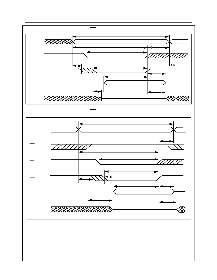
FIGURE 5: Write Cycle Timing (OE fixed)
FIGURE 6: Write Cycle Timing (OE clock)
A0-A14
CE
WE
Data In
Data Out
t
WP
t
DW
t
DH
Data Valid
High-Z
t
WHZ
t
OW
t
WC
t
AW
t
CW
t
WR
t
AS
t
OH
A0-A14
OE
CE
WE
Data In
Data Out
t
WC
t
A W
t
CW
t
W P
t
WHZ
t
DW
t
DH
Data
High-Z
t
W R
t
OHZ
t
O W
t
AS
Stock No. 23087-03 12/00
Subject to change without notice
6
EM033C08
NanoAmp Solutions, Inc.
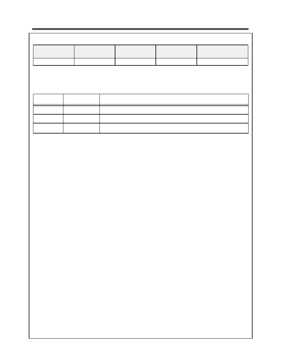
TABLE 7: Ordering Information
* Please use this part number when ordering this product. This number will be marked on the device package.
TABLE 8: Revision History
� 1998-2001 Nanoamp Solutions, Inc. All rights reserved.
NanoAmp Solutions, Inc. ("NanoAmp") reserves the right to change or modify the in-
formation contained in this datasheet and the products described therein, without prior
notice. NanoAmp does not convey any license under its patent rights nor the rights of
others. Charts, drawings and schedules contained in this datasheet are provided for
illustration purposes only and they vary depending upon specific applications.
NanoAmp makes no warranty or guarantee regarding suitability of these products for
any particular purpose, nor does NanoAmp assume any liability arising out of the ap-
plication or use of any product or circuit described herein. NanoAmp does not autho-
rize use of its products as critical components in any application in which the failure of
the NanoAmp product may be expected to result in significant injury or death, including
life support systems and critical medical instruments.
Part Number*
Package
Temperature
Range
Voltage
Range
Speed (@ 2.7V+)
EM033C08N
32 pin STSOP
-20 to +80
o
C
1.5 to 3.6 V
100 ns
Revision #
Date
Change Description
01
Dec 98
Initial Release
02
Oct 00
Tie pin 30 to Vcc
03
Dec 00
Tie pins 6, 10, 11 to Vss, eliminated T
ASC
and T
AHC