Stock No. 23149-04 09/01
Preliminary - Subject to Change Without Notice
1
EM128P16
Preliminary
NanoAmp Solutions, Inc.
1982 Zanker Road, San Jose, CA 95112
ph: 408-573-8878, FAX: 408-573-8877
www.nanoamp.com
EM128P16 Family
128Kx16 bit Ultra-Low Power Asynchronous Static RAM
Overview
The EM128P16 is an integrated memory device
containing a low power 2 Mbit Static Random
Access Memory organized as 131,072 words by 16
bits. The device is fabricated using NanoAmp's
advanced CMOS process and high-speed/ultra
low-power/low-voltage circuit technology. The
device pinout is compatible with other standard
128K x 16 SRAMs.
Designed for compatibility with the Intersil PRISM
chipset.
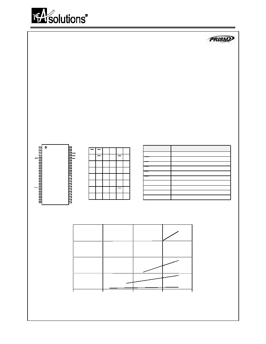
FIGURE 1: Pin Configurations
Features
�
Wide Voltage Range:
2.7 to 3.6 Volts
�
Extended Temperature Range:
-40 to +85
o
C
�
Fast Cycle Time:
T
ACC
< 35 ns @ 2.7V
�
Very Low Operating Current:
I
CC
< 5 mA typical at 3.3V, 10 Mhz
�
Very Low Standby Current:
I
SB
= 1
�
�
A
typical @ 55
o
C
�
44-Pin TSOP, 48-Pin BGA Available
TABLE 1: Pin Descriptions
FIGURE 2: Operating Envelope
PIN
ONE
1
2
3
4
5
6
7
8
9
10
11
12
13
14
15
16
17
18
19
20
21
22
A
4
A
3
A
2
A
1
A
0
C E
I/O
0
I/O
1
I/O
2
I/O
3
VCC
VSS
I/O
4
I/O
5
I/O
6
I/O
7
WE
A
16
A
15
A
14
A
13
A
12
44
43
42
41
40
39
38
37
36
35
34
33
32
31
30
29
28
27
26
25
24
23
A
5
A
6
A
7
OE
U B
L B
I/O
15
I/O
14
I/O
13
I/O
12
VSS
VCC
I/O
11
I/O
10
I/O
9
I/O
8
NC
A
8
A
9
A
10
A
11
NC
E
M
1
2
8
P
1
6
T
T
S
O
P
LB
OE
A
0
A
1
A
2
NC
I/O
8
UB
A
3
A
4
C E
I/O
0
I/O
9
I/O
10
A
5
A
6
I/O
1
I/O
2
V
SS
I/O
11
NC
A
7
I/O
3
V
CC
V
CC
I/O
12
NC
A
16
I/O
4
V
SS
I/O
14
I/O
13
A
14
A
15
I/O
5
I/O
6
I/O
15
NC
A
12
A
13
WE
I/O
7
NC
A
8
A
9
A
10
A
11
NC
48 Pin BGA (top)
A
B
C
D
E
F
G
H
1 2 3 4 5 6
6 x 8 mm
Pin Name
Pin Function
A
0
-A
16
Address Inputs
WE
Write Enable Input
CE
Chip Enable Input
OE
Output Enable Input
LB
Lower Byte Enable Input
UB
Upper Byte Enable Input
I/O
0
-I/O
15
Data Inputs/Outputs
NC
Not Connected
V
C C
Power
V
SS
Ground
20
5
T
y
p
i
c
a
l
I
C
C
(
m
A
)
40 MHz
10 MHz
1 MHz
V
CC
(V)
20 MHz
15
0
1
2
3
4
10
0
Stock No. 23149-04 09/01
Preliminary - Subject to Change Without Notice
2
NanoAmp Solutions, Inc.
EM128P16
Preliminary
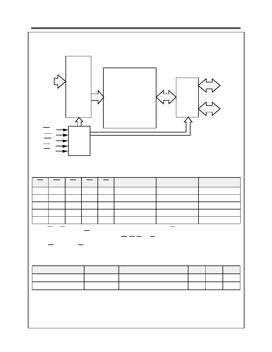
FIGURE 3: Functional Block Diagram
TABLE 2: Functional Description
1. When UB and LB are in select mode (low), I/O
0
- I/O
15
are affected as shown. When LB only is in the select mode only I/O
0
- IO
7
are affected as shown. When UB is in the select mode only I/O
8
- I/O
15
are affected as shown.
2. When the device is in standby mode, control inputs (WE, OE, UB, and LB), address inputs and data input/outputs are internally
isolated from any external influence and disabled from exerting any influence externally.
3. When WE is invoked, the OE input is internally disabled and has no effect on the circuit.
4. The device will consume active power in this mode whenever addresses are changed. Data inputs are internally isolated from any
external influence.
TABLE 3: Capacitance*
Note: These parameters are verified in device characterization and are not 100% tested
Control
Logic
Decode
Logic
Address
Inputs
A
0
- A
17
CE
WE
OE
Input/
Output
Mux
and
Buffers
I/O
0
- I/O
7
UB
LB
I/O
8
- I/O
15
Address
128K x 16
Memory
Array
CE
WE
OE
UB
LB
I/O
0
- I/O
15
1
MODE
POWER
H
X
X
X
X
High Z
Standby
2
Standby
X
X
X
H
H
High Z
Active
Active
L
L
X
3
L
1
L
1
Data In
Write
3
Active -> Standby
4
L
H
L
L
1
L
1
Data Out
Read
Active -> Standby
4
L
H
H
L
1
L
1
High Z
Active
Standby
4
Item
Symbol
Test Condition
Min
Max
Unit
Input Capacitance
C
IN
V
IN
= 0V, f = 1 MHz, T
A
= 25
o
C
8
pF
I/O Capacitance
C
I/O
V
IN
= 0V, f = 1 MHz, T
A
= 25
o
C
8
pF
Stock No. 23149-04 09/01
Preliminary - Subject to Change Without Notice
3
NanoAmp Solutions, Inc.
EM128P16
Preliminary
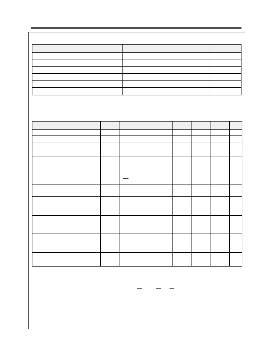
TABLE 4: Absolute Maximum Ratings*
* Stresses greater than those listed above may cause permanent damage to the device. This is a stress rating only and functional
operation of the device at these or any other conditions above those indicated in the operating section of this specification is not
implied. Exposure to absolute maximum rating conditions for extended periods may affect reliability.
TABLE 5: Operating Characteristics (Over specified Temperature Range)
1. Operating current is a linear function of operating frequency and voltage. You may calculate operating current using the formul a
shown with operating frequency (f) expressed in MHz and operating voltage (V) in volts. Example: When operating at 10 MHz at
3.0 volts the device will draw a maximum active current of 0.2*3*10 = 6.0 mA. This parameter is specified with the outputs dis-
abled to avoid external loading effects. The user must add current required to drive output capacitance expected in the actual s ys-
tem.
2. This device assumes a standby mode if the chip is disabled (CE high or UB and LB high). It will also automatically go into a
standby mode whenever all input signals are quiescent (not toggling) regardless of the state of CE, UB and LB. In order to
achieve low standby current all inputs must be within 0.2 volts of either VCC or VSS.
3. The Chip is Disabled when CE is high or when both UB and LB are high. The Chip is Enabled when CE is low and UB or LB are
low.
Item
Symbol
Rating
Unit
Voltage on any pin relative to V
SS
V
IN,OUT
�0.3 to V
CC
+0.3
V
Voltage on V
CC
Supply Relative to V
SS
V
CC
�0.3 to 4.0
V
Power Dissipation
P
D
500
mW
Storage Temperature
T
STG
-40 to 125
o
C
Operating Temperature
T
A
-40 to +85
o
C
Soldering Temperature and Time
T
SOLDER
260
o
C, 10sec(Lead only)
o
C
Item
Symbol
Test Conditions
Min
Typ
Max
Unit
Supply Voltage
V
CC
2.7
3.6
V
Data Retention Voltage
V
DR
Chip Disabled (Note 3)
1.8
V
Input High Voltage
V
IH
0.7V
CC
V
CC
+0.5
V
Input Low Voltage
V
IL
�0.5
0.3V
CC
V
Output High Voltage
V
OH
I
OH
= 0.2mA
V
CC
�0.3
V
Output Low Voltage
V
OL
I
OL
= -0.2mA
0.3
V
Input Leakage Current
I
LI
V
IN
= 0 to V
CC
0.5
�
A
Output Leakage Current
I
LO
OE = V
IH
or Chip Disabled
0.5
�
A
Read/Write Operating Supply Cur-
rent (Note 1)
I
CC1
V
IN
= V
IH
or V
IL
Chip Enabled, IOL = 0
0.25fV
mA
Read/Write Quiescent Operating
Supply Current (Note 2)
I
CC3
V
IN
= V
CC
or 0V
Chip Enabled, IOL = 0 f = 0,
t
A
= 85
o
C, VCC = 3.6 V
40
�
A
Operating Standby Current
(Note 2)
I
SB1
V
IN
= V
CC
or 0V
Chip Disabled
t
A
= 55
o
C, VCC = 3.3V
1
�
A
Maximum Standby Current
(Note 2)
I
SB2
V
IN
= V
CC
or 0V
Chip Disabled
t
A
= 85
o
C, VCC = 3.6V
40
�
A
Maximum Data Retention Current
(Note 2)
I
DR
Vcc = 2.0V, V
IN
= V
CC
or 0
Chip Disabled, t
A
= 85
o
C
10
�
A
Stock No. 23149-04 09/01
Preliminary - Subject to Change Without Notice
4
NanoAmp Solutions, Inc.
EM128P16
Preliminary
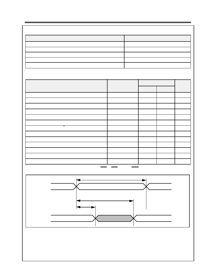
TABLE 6: Timing Test Conditions
TABLE 7: Read Cycle Timing
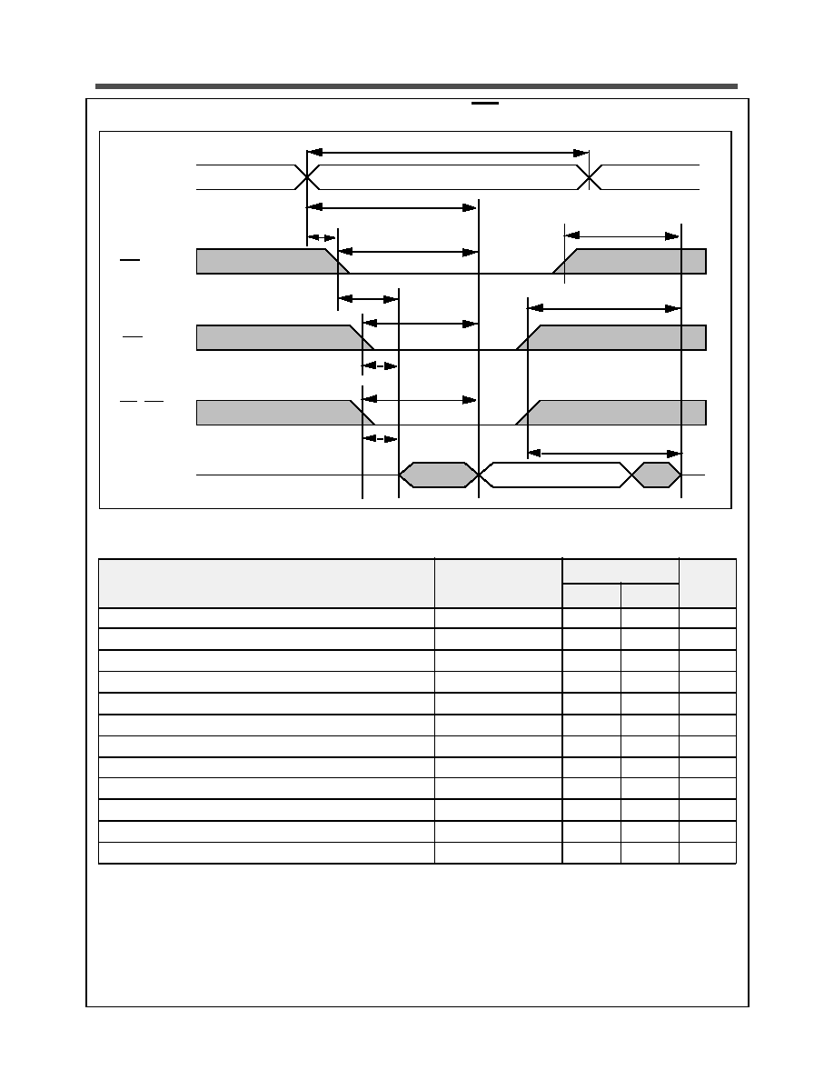
FIGURE 4: Timing of Read Cycle (1) (CE = OE = V
IL
, WE = V
IH
)
Item
Input Pulse Level
0.1V
CC
to 0.9 V
CC
Input Rise and Fall Time
5ns
Input and Output Timing Reference Levels
0.5 V
CC
Output Load
CL = 30pF
Operating Temperature
-40 to +85
o
C
Item
Symbol
2.7 - 3.6 V
Units
Min.
Max.
Read Cycle Time
t
RC
35
ns
Address Access Time
t
AA
35
ns
Chip Enable to Valid Output
t
CO
35
ns
Output Enable to Valid Output
t
OE
20
ns
Byte Select to Valid Output
t
LB
, t
UB
35
ns
Read Address Setup
t
ASR
-2
ns
Chip Enable to Low-Z output
t
LZ
5
ns
Output Enable to Low-Z Output
t
OLZ
3
ns
Byte Select to Low-Z Output
t
LBZ
, t
UBZ
3
ns
Chip Disable to High-Z Output
t
HZ
15
ns
Output Disable to High-Z Output
t
OHZ
15
ns
Byte Select Disable to High-Z Output
t
LBHZ
, t
UBHZ
15
ns
Output Hold from Address Change
t
OH
5
ns
Address
Data Out
t
RC
t
AA
t
OH
Data Valid
Previous Data Valid
Stock No. 23149-04 09/01
Preliminary - Subject to Change Without Notice
5
NanoAmp Solutions, Inc.
EM128P16
Preliminary
FIGURE 5: Timing Waveform of Read Cycle (2) (WE = V
IH
)
TABLE 8: Write Cycle Timing
Item
Symbol
2.7 - 3.6 V
Units
Min.
Max.
Write Cycle Time
t
WC
35
ns
Chip Enable to End of Write
t
CW
35
ns
Address Valid to End of Write
t
AW
20
ns
Byte Select to End of Write
t
LBW
, t
UBW
35
ns
Write Pulse Width
t
WP
20
ns
Address Setup Time
t
AS
0
ns
Byte Select Setup Time
t
LBWS
, t
UBWS
0
ns
Write Recovery Time
t
WR
0
ns
Write to High-Z Output
t
WHZ
10
ns
Data to Write Time Overlap
t
DW
20
ns
Data Hold from Write Time
t
DH
0
End Write to Low-Z Output
t
OW
5
ns
Address
LB, UB
OE
Data Valid
t
RC
t
AA
t
CO
t
HZ(1,2)
t
OHZ(1)
t
LBHZ,
t
UBHZ
t
OLZ
t
OE
t
LZ(2)
High-Z
Data Out
t
LB,
t
UB
t
LBLZ,
t
UBLZ
CE
t
ASR

Stock No. 23149-04 09/01
Preliminary - Subject to Change Without Notice
6
NanoAmp Solutions, Inc.
EM128P16
Preliminary
FIGURE 6: Timing Waveform of Write Cycle (1) (WE control)
FIGURE 7: Timing Waveform of Write Cycle (2) (CE Control)
Address
Data In
CE
LB, UB
Data Valid
t
WC
t
AW
t
CW
t
WR
t
WHZ
t
DH
High-Z
WE
Data Out
High-Z
t
O W
t
A S
t
WP
t
DW
t
LBW
, t
UBW
t
LBWS
, t
UBWS
Address
WE
Data Valid
t
W C
t
AW
t
CW
t
W R
t
DH
LB, UB
Data In
High-Z
t
A S
t
WP
t
LZ
t
DW
t
LBW
, t
UBW
Data Out
t
WHZ
CE
t
LBWS
, t
UBWS

Stock No. 23149-04 09/01
Preliminary - Subject to Change Without Notice
7
NanoAmp Solutions, Inc.
EM128P16
Preliminary
FIGURE 8: 44-LEAD TSOP PACKAGE (T44)
Note:
1. ALL DIMENSIONS IN INCHES (MILLIMETERS)
2. PACKAGE DIMENSIONS EXCLUDE MOLDING FLASH
P
I
N
O
N
E
0.730(18.53)
0.720(18.23)
0.405(10.28)
0.395(10.03)
SEE DETAIL B
0.049(1.25)
0.037(.939)
0.471(11.95)
0.455(11.55)
0.018(.457)
0.012(.305)
0.031(.800)
DETAIL B
0.024(.61)
0.016(.407)
0
o
-5
o
0.010(.254)
0.005(.127)
0.008(0.20)
0.000(0.00)

Stock No. 23149-04 09/01
Preliminary - Subject to Change Without Notice
8
NanoAmp Solutions, Inc.
EM128P16
Preliminary
FIGURE 9: BALL GRID ARRAY PACKAGING
TABLE 9: Dimensions (mm)
SIDE VIEW
TOP VIEW
BOTTOM VIEW
E
D
A1 BALL PAD
CORNER (3)
0.70�0.05
1.24 max.
0.20�0.04
0.15
0.05
Z
Z
1. .30 DIA. TYP
1. DIMENSION IS MEASURED AT THE
MAXIMUM SOLDER BALL DIAMETER.
PARALLEL TO PRIMARY Z.
2. PRIMARY DATUM Z AND SEATING
PLANE ARE DEFINED BY THE SPHERI-
CAL CROWNS OF THE SOLDER
BALLS.
3. A1 BALL PAD CORNER I.D. TO BE
MARKED BY INK.
2. SEATING PLANE - Z
SD
SE
e
K TYP
J TYP
e
A1 BALL PAD
CORNER
D
E
e = 0.75
BALL
MATRIX
TYPE
SD
SE
J
K
6
8
0.375
0.375
1.125
1.375
FULL
Stock No. 23149-04 09/01
Preliminary - Subject to Change Without Notice
9
NanoAmp Solutions, Inc.
EM128P16
Preliminary
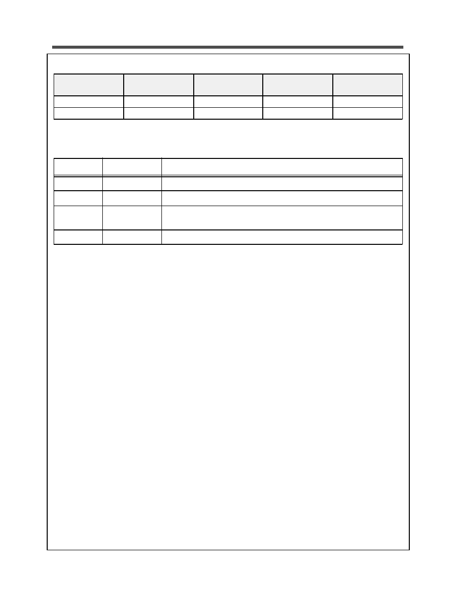
TABLE 10: Ordering Information
* This part number must appear on your order.
TABLE 11: Revision History
� 2001 Nanoamp Solutions, Inc. All rights reserved. PRISM is a registered trademark
of Intersil Americas, Inc.
NanoAmp Solutions, Inc. ("NanoAmp") reserves the right to change or modify the in-
formation contained in this datasheet and the products described therein, without prior
notice. NanoAmp does not convey any license under its patent rights nor the rights of
others. Charts, drawings and schedules contained in this datasheet are provided for
illustration purposes only and they vary depending upon specific applications.
NanoAmp makes no warranty or guarantee regarding suitability of these products for
any particular purpose, nor does NanoAmp assume any liability arising out of the ap-
plication or use of any product or circuit described herein. NanoAmp does not autho-
rize use of its products as critical components in any application in which the failure of
the NanoAmp product may be expected to result in significant injury or death, including
life support systems and critical medical instruments.
Part Number*
Package
Temperature
Range
Voltage
Range
Speed
EM128P16B
48 pin BGA
-40 to +85
o
C
2.7 to 3.6 V
35 ns
EM128P16T
44 pin TSOP
-40 to +85
o
C
2.7 to 3.6 V
35 ns
Revision #
Date
Change Description
01
June 2001
Initial Preliminary Release
02
August 2001
Modified cycle time, other minor edits
03
August 2001
Modified Figure 1 (BGA), Table 2, Table 5, Figure 6, Figure 8, Figure
9, voltage range, cycle time
04
Sept 2001
Added read address setup