NanoAmp Solutions, Inc.
1982 Zanker Road, San Jose, CA 95112
ph: 408-573-8878, FAX: 408-573-8877
www.nanoamp.com
N01L0850C2A
Stock No. 23172-02 11/02
1
The specifications of this device are subject to change without notice. For latest documentation see http://www.nanoamp.com.
1Mb Ultra-Low Power Asynchronous CMOS SRAM
128Kx8 bit
Overview
The N01L0850C2A is an integrated memory
device containing a 1 Mbit Static Random Access
Memory organized as 131,072 words by 8 bits. The
device is designed and fabricated using
NanoAmp's advanced CMOS technology to
provide both high-speed performance and ultra-low
power. The device operates with two chip enable
(CE1 and CE2) controls and output enable (OE) to
allow for easy memory expansion. The
N01L0850C2A is optimal for various applications
where low-power is critical such as battery backup
and hand-held devices. The device can operate
over a very wide temperature range of -40
o
C to
+85
o
C and is available in a JEDEC standard 32-pin
SOP package.
Features
∑ Wide Power Supply Range
4.5 to 5.5 Volts Very low standby current
0.8µA at 5.0V (Typical)
∑ Very low operating current
10.0mA at 5.0V and 1µs (Typical)
∑ Simple memory control
Dual Chip Enables (CE1and CE2)
Output Enable (OE) for memory expansion
∑ Low voltage data retention
Vcc = 1.5V
∑ Very fast output enable access time
40ns OE access time
∑ Automatic power down to standby mode
∑ TTL compatible three-state output driver
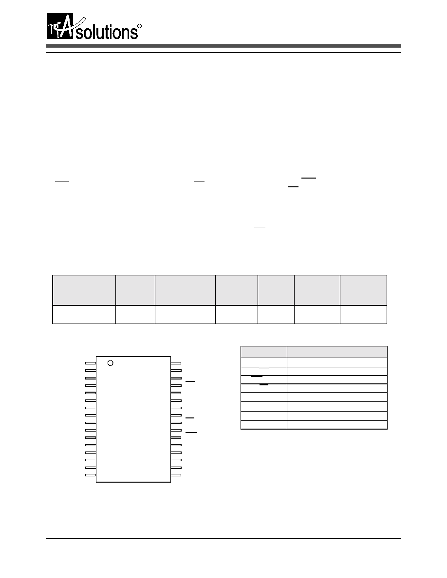
Pin Configuration
Product Family
Part Number
Package
Type
Operating
Temperature
Power
Supply (Vcc)
Speed
Standby
Current (I
SB
),
Typical
Operating
Current (Icc),
Typical
N01L0850C2AS-70I 32 - SOP I
-40
o
C to +85
o
C
4.5V - 5.5V
70ns
0.8
µ
A
10 mA @
1MHz
N01L0850C2A
SOP
NC
A16
A14
A12
A7
A6
A5
A4
A3
A2
A1
A0
I/O0
I/O1
I/O2
Vss
Vcc
A15
CE2
WE
A13
A8
A9
A11
OE
A10
CE1
I/O7
I/O6
I/O5
I/O4
I/O3
1
2
3
4
5
6
7
8
9
10
11
12
13
14
15
16
32
31
30
29
28
27
26
25
24
23
22
21
20
19
18
17
Pin Descriptions
Pin Name
Pin Function
A
0
-A
16
Address Inputs
WE
Write Enable Input
CE1, CE2
Chip Enable Input
OE
Output Enable Input
I/O
0
-I/O
7
Data Inputs/Outputs
V
CC
Power
V
SS
Ground
NC
Not Connected
Stock No. 23172-02 11/02
2
The specifications of this device are subject to change without notice. For latest documentation see http://www.nanoamp.com.
NanoAmp Solutions, Inc.
N01L0850C2A
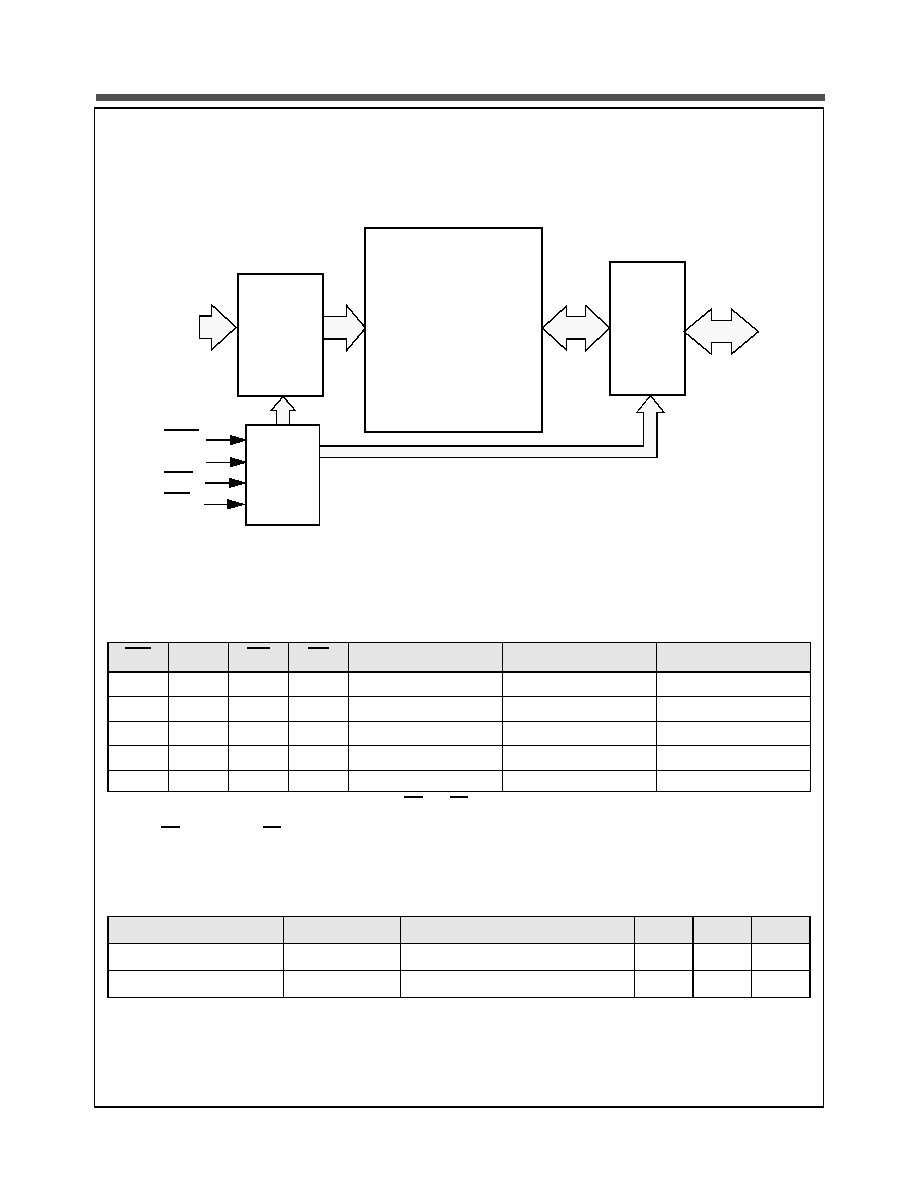
Functional Block Diagram
Functional Description
CE1
CE2
WE
OE
I/O
0
- I/O
7
MODE
POWER
H
X
X
X
High Z
Standby
1
1. When the device is in standby mode, control inputs (WE and OE), address inputs and data input/outputs are internally isolated
from any external influence and disabled from exerting any influence externally.
Standby
X
L
X
X
High Z
Standby
1
Standby
L
H
L
X
2
2. When WE is invoked, the OE input is internally disabled and has no effect on the circuit.
Data In
Write
2
Active
L
H
H
L
Data Out
Read
Active
L
H
H
H
High Z
Active
Active
Capacitance
1
1. These parameters are verified in device characterization and are not 100% tested
Item
Symbol
Test Condition
Min
Max
Unit
Input Capacitance
C
IN
V
IN
= 0V, f = 1 MHz, T
A
= 25
o
C
6
pF
I/O Capacitance
C
I/O
V
IN
= 0V, f = 1 MHz, T
A
= 25
o
C
8
pF
Control
Logic
Decode
Logic
Address
Inputs
A
0
- A
16
Input/
Output
Mux
and
Buffers
I/O
0
- I/O
7
Address
128K x 8 bit
RAM Array
CE1
CE2
WE
OE

Stock No. 23172-02 11/02
3
The specifications of this device are subject to change without notice. For latest documentation see http://www.nanoamp.com.
NanoAmp Solutions, Inc.
N01L0850C2A
Absolute Maximum Ratings
1
1. Stresses greater than those listed above may cause permanent damage to the device. This is a stress rating only and functional
operation of the device at these or any other conditions above those indicated in the operating section of this specification is not
implied. Exposure to absolute maximum rating conditions for extended periods may affect reliability.
Item
Symbol
Rating
Unit
Voltage on any pin relative to V
SS
V
IN,OUT
≠0.5 to V
CC
+0.5
V
Power Dissipation
P
D
600
mW
Storage Temperature
T
STG
≠40 to 125
o
C
Operating Temperature
T
A
-40 to +85
o
C
Soldering Temperature and Time
T
SOLDER
240
o
C, 10sec(Lead only)
o
C
Operating Characteristics (Over Specified Temperature Range)
Item
Symbol
Test Conditions
Min.
Typ
1
1. Typical values are measured at Vcc=Vcc Typ., T
A
=25∞C and not 100% tested.
Max
Unit
Supply Voltage
V
CC
4.5
5.0
5.5
V
Data Retention Voltage
V
DR
Chip Disabled
2
1.5
V
Input High Voltage
V
IH
2.2
V
CC
+0.2
V
Input Low Voltage
V
IL
≠0.5
0.8
V
Output High Voltage
V
OH
I
OH
= 1mA
2.4
V
Output Low Voltage
V
OL
I
OL
= -2mA
0.4
V
Input Leakage Current
I
LI
V
IN
= 0 to V
CC
1
µ
A
Output Leakage Current
I
LO
OE = V
IH
or Chip Disabled
1
µ
A
Read/Write Operating Supply Current
@ 70 nS Cycle Time
2
I
CC2
V
CC
=5.0 V, V
IN
=V
IH
or V
IL
Chip Enabled, I
OUT
= 0
35.0
mA
Maximum Standby Current
2
2. This device assumes a standby mode if the chip is disabled (CE1 high or CE2 low). In order to achieve low standby current all
inputs must be within 0.2 volts of either VCC or VSS.
I
SB
VIN
Vcc-0.2V or
0.2V
Chip Disabled
t
A
= 85
o
C, V
CC
= 3.6 V
0.8
5
µ
A
Maximum Data Retention Current
2
I
DR
VIN
Vcc-0.2V or
0.2V
Chip Disabled, t
A
= 85
o
C
0.5
µ
A

Stock No. 23172-02 11/02
4
The specifications of this device are subject to change without notice. For latest documentation see http://www.nanoamp.com.
NanoAmp Solutions, Inc.
N01L0850C2A
Timing Test Conditions
Item
Input Pulse Level
0.1V
CC
to 0.9 V
CC
Input Rise and Fall Time
5ns
Input and Output Timing Reference Levels
0.5 V
CC
Output Load
CL = 100pF
Operating Temperature
-40 to +85
o
C
Timing
Item
Symbol
Min
Max
Units
Read
Cycle
Read Cycle Time
t
RC
70
ns
Address Access Time
t
AA
70
ns
Chip Enable to Valid Output
t
CO
70
ns
Output Enable to Valid Output
t
OE
40
ns
Chip Enable to Low-Z output
t
LZ
10
ns
Output Enable to Low-Z Output
t
OLZ
10
ns
Chip Disable to High-Z Output
t
HZ
0
40
ns
Output Disable to High-Z Output
t
OHZ
0
35
ns
Output Hold from Address Change
t
OH
10
ns
Write
Cycle
Write Cycle Time
t
WC
70
ns
Chip Enable to End of Write
t
CW
70
ns
Address Valid to End of Write
t
AW
70
ns
Write Pulse Width
t
WP
50
ns
Address Setup Time
t
AS
0
ns
Write Recovery Time
t
WR
0
ns
Write to High-Z Output
t
WHZ
30
ns
Data to Write Time Overlap
t
DW
30
ns
Data Hold from Write Time
t
DH
0
ns
End Write to Low-Z Output
t
OW
5
ns

Stock No. 23172-02 11/02
5
The specifications of this device are subject to change without notice. For latest documentation see http://www.nanoamp.com.
NanoAmp Solutions, Inc.
N01L0850C2A
Timing of Read Cycle (CE1 = OE = V
IL
, WE = CE2 = V
IH
)
Timing Waveform of Read Cycle (WE=V
IH
)
Address
Data Out
t
RC
t
AA
t
OH
Data Valid
Previous Data Valid
Address
OE
Data Valid
t
RC
t
AA
t
CO
t
HZ
t
OHZ
t
OLZ
t
OE
t
LZ
High-Z
Data Out
CE1
CE2

Stock No. 23172-02 11/02
6
The specifications of this device are subject to change without notice. For latest documentation see http://www.nanoamp.com.
NanoAmp Solutions, Inc.
N01L0850C2A
Timing Waveform of Write Cycle (WE control)
Timing Waveform of Write Cycle (CE1 Control)
Address
Data In
CE1
CE2
Data Valid
t
WC
t
AW
t
CW
t
WR
t
WHZ
t
DH
High-Z
WE
Data Out
High-Z
t
OW
t
AS
t
WP
t
DW
Address
WE
Data Valid
t
WC
t
AW
t
CW
t
WR
t
DH
Data In
High-Z
t
AS
t
WP
t
LZ
t
DW
Data Out
t
WHZ
CE1
(for CE2 Control, use
inverted signal)

Stock No. 23172-02 11/02
7
The specifications of this device are subject to change without notice. For latest documentation see http://www.nanoamp.com.
NanoAmp Solutions, Inc.
N01L0850C2A
Timing Waveform for Data Retention Mode
Data Retention Characteristics
Item
Symbol
Test Conditions
Min.
Max
Unit
Power Supply Vcc
V
DR
CE1
Vcc-0.2V, CE2
0.2V,
VIN
Vcc-0.2V or
0.2V
1.5
V
Data Retention Current
I
CCDR
CE1
Vcc-0.2V, CE2
0.2V,
VIN
Vcc-0.2V or
0.2V
0.5
µ
A
Chip Disabled to Data Retention Time
t
cdr
0
nS
Data Retention Recovery Time
t
r
70
ns
Vcc
CE1
t
cdr
t
r
Data Retention Mode
Vcc
Vcc
VIH
VIH
Vcc
CE2
t
cdr
t
r
Data Retention Mode
Vcc
Vcc
VIL
VIL
CE1
Vcc-0.2V
CE2
0.2V
VDR
1.5V
VDR
1.5V

Stock No. 23172-02 11/02
8
The specifications of this device are subject to change without notice. For latest documentation see http://www.nanoamp.com.
NanoAmp Solutions, Inc.
N01L0850C2A
32-Lead SOP Package
Note:
1. All dimensions in millimeters
20.447±0.127
14.097±0.305
11.303±0.127
0.35 - 0.50
1.397±0.203
0
o
-10
o
1.27±0.152
0.834±0.25
0.229±0.127
2.680±0.140
2.821±0.176
Seating plane - 0.1 max
Stock No. 23172-02 11/02
9
The specifications of this device are subject to change without notice. For latest documentation see http://www.nanoamp.com.
NanoAmp Solutions, Inc.
N01L0850C2A
Ordering Information
© 1999 - 2001 Nanoamp Solutions, Inc. All rights reserved.
NanoAmp Solutions, Inc. ("NanoAmp") reserves the right to change or modify the information contained in this data sheet and the products described therein, without prior notice.
NanoAmp does not convey any license under its patent rights nor the rights of others. Charts, drawings and schedules contained in this data sheet are provided for illustration pur-
poses only and they vary depending upon specific applications.
NanoAmp makes no warranty or guarantee regarding suitability of these products for any particular purpose, nor does NanoAmp assume any liability arising out of the application
or use of any product or circuit described herein. NanoAmp does not authorize use of its products as critical components in any application in which the failure of the NanoAmp
product may be expected to result in significant injury or death, including life support systems and critical medical instruments.
Revision History
Revision #
Date
Change Description
01
Sept 2002
Initial Release
02
Nov. 2002
Replaced Isb and Icc on Product Family table with typical values
N01L0850C2AS-70I