1
Stock No. 23134-E 9/02
N02C1630E1AM
Advance Information
Advance - Subject to Change without Notice
NanoAmp Solutions, Inc.
1982 Zanker Road, San Jose, CA 95112
ph: 408-573-8878, FAX: 408-573-8877
www.nanoamp.com
FLASH AND SRAM COMBO MEMORY
N02C1630E1AM
Low Voltage, Extended Temperature
FEATURES
∑ Organization: 1,048K x 16 (Flash)
128K x 16 (SRAM)
∑ Basic configuration:
Flash
Thirty-nine erase blocks
≠ Eight 4K-word parameter blocks
≠ Thirty-one 32K-word main memory blocks
SRAM
2Mb SRAM for data storage
≠ 128K-words
∑ F_V
CC
, F_V
PP
, S_V
CC
voltages
2.7V (MIN)/3.3V (MAX) F_V
CC
read voltage
2.7V (MIN)/3.3V (MAX) S_V
CC
read voltage
1.8V (TYP) F_V
PP
(in-system PROGRAM/ERASE)
12V ±5% (HV) F_V
PP
(production programming
compatibility)
1.0V (MIN) S_V
CC
(SRAM data retention)
∑ Asynchronous access time
Flash access time: 90ns @ 2.7V F_V
CC
SRAM access time: 85ns @ 2.7V S_V
CC
∑ Low power consumption
∑ Enhanced WRITE/ERASE suspend option
∑ Read/Write SRAM during program/erase of Flash
∑ 128-bit chip OTP protection register for security
purposes
∑ Cross-compatible command set support
∑ PROGRAM/ERASE cycles
100,000 WRITE/ERASE cycles per block
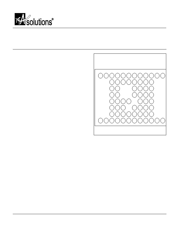
BALL ASSIGNMENT
66-Ball FBGA (Top View)
OPTIONS
MARKING
∑ Timing
90ns
-9
∑ Boot Block
Top
T
Bottom
B
∑ Operating Temperature Range
Industrial Temperature (-40
o
C to +85
o
C)
I
Part Number Example:
N02C1630E1AM-9TI
NC
F_WE #
NC
NC
A16
S_Vss
F_WP #
S_LB#
A18
A11
A15
A14
A13
A12
F_Vss
NC
NC
1 2 3 4 5
6 7 8
9 10 11
12
A
B
C
D
E
F
G
H
A8
A10
A9
NC
F_RP#
F_Vpp
S_UB#
A17
A5
NC
NC
NC
NC
NC
S_OE #
A7
A4
A19
DQ15
DQ13
DQ12
S_W E#
DQ11
DQ9
A6
A0
A3
F_CE#
DQ6
S_CE2
DQ10
DQ8
A2
F_Vss
DQ14
DQ4
S_Vcc
DQ2
DQ0
A1
F_OE#
DQ7
DQ5
F_Vcc
DQ3
DQ1
S_CE1#
NC
NC
NC
F_WE #
NC
NC
A16
S_Vss
F_WP #
S_LB#
A18
A11
A15
A14
A13
A12
F_Vss
NC
NC
1 2 3 4 5
6 7 8
9 10 11
12
A
B
C
D
E
F
G
H
A8
A10
A9
NC
F_RP#
F_Vpp
S_UB#
A17
A5
NC
NC
NC
NC
NC
S_OE #
A7
A4
A19
DQ15
DQ13
DQ12
S_W E#
DQ11
DQ9
A6
A0
A3
F_CE#
DQ6
S_CE2
DQ10
DQ8
A2
F_Vss
DQ14
DQ4
S_Vcc
DQ2
DQ0
A1
F_OE#
DQ7
DQ5
F_Vcc
DQ3
DQ1
S_CE1#
NC
NC

2
Stock No. 23134-E 9/02
N02C1630E1AM
Advance
NanoAmp Solutions, Inc.
Advance - Subject to Change without Notice
GENERAL DESCRIPTION
The N02C1630E1AM, a combination of Flash and
SRAM memory, provides a compact, low-power
solution for systems where PCB real estate is at a
premium. The device contains a nonvolatile, electrically
block-erasable (flash), programmable, read-only memory
containing 16,777,216 bits organized as 1,048,576 words
(16 bits).
The device also provides soft protection for blocks by
configuring soft protection registers with dedicated com-
mand sequences. A 128-bit (OTP )one time programmable
register is provided.
The embedded WORD WRITE and BLOCK ERASE
functions are fully automated by an on-chip write state
machine (WSM). The WSM simplifies these operations and
relieves the system processor of secondary tasks. An
on-chip status register, can be used to monitor the WSM
status to determine the progress of a PROGRAM/ERASE
command.
The erase/program suspend functionality allows com-
patibility with existing EEPROM emulation software pack-
ages.
The device takes advantage of a dedicated power
source for the Flash device (F_V
CC
) and a dedicated
power source for the SRAM device (S_V
CC
), both at
2.7V≠3.3V for optimized power consumption and im-
proved noise immunity. The separate S_V
CC
pin for the
SRAM provides the data retention capability whenever
required. The data retention S_V
CC
is specified as low as
1.0V. The device supports two V
PP
voltages; in-circuit
V
PP
of 1.65V≠3.3V and production compatibility of 12V
±5%. The 12V ±5% V
PP
is supported for a maximum of 100
cycles and 10 cumulative hours.
The N02C1630E1AM contains an asynchronous 2Mb
SRAM organized as 128K-words by 16 bits. This device
is fabricated using an advanced CMOS process and high-
speed/ultra-low-power circuit technology.
The N02C1630E1AM is packaged in a 66-ball FBGA
package with 0.80mm pitch.

3
Stock No. 23134-E 9/02
N02C1630E1AM
Advance
NanoAmp Solutions, Inc.
Advance - Subject to Change without Notice
PART NUMBERING INFORMATION
NanoAmp's low-power devices are available with
several different combinations of features. Valid combi-
nations of features and their corresponding part numbers
are listed in Table 1.
Part Number Chart
N 02 C 16 30 E1 A M - 9T I
Die Revision
Package Type
Flash Density
NanoAmp Solutions
SRAM Density
I/O Organization
Operating Voltage
Flash/SRAM Combo
Performance & Boot Block
Operating Temperature
Table 1
Valid Part Number Combinations
BOOT
OPERATING
ACCESS
BLOCK
TEMPERATURE
PART NUMBER
TIME (ns)
RANGE
N02C1630E1AM-9BI
90
Bottom
-40
o
C to +85
o
C
N02C1630E1AM-9TI
90
Top
-40
o
C to +85
o
C

4
Stock No. 23134-E 9/02
N02C1630E1AM
Advance
NanoAmp Solutions, Inc.
Advance - Subject to Change without Notice
FLASH FUNCTIONAL BLOCK DIAGRAM
Address
Input
Buffer
X DEC
Y/Z DEC
Data Input
Buffer
APS
Control
Data
Comparator
Output
Multiplexer
Address
CNT WSM
Output
Buffer
Status
Reg.
ID
Reg.
WSM
Program/
Erase Change
Pump Voltage
Switch
Address Latch
DQ0-DQ15
DQ0-DQ15
CSM
RP#
CE#
X DEC
Y/Z DEC
WE#
OE#
I/O Logic
A0-A19
Address
Multiplexer
Bank b Blocks
Y/Z Gating/Sensing
Data
Register
Bank a Blocks
Y/Z Gating/Sensing
5
Stock No. 23134-E 9/02
N02C1630E1AM
Advance
NanoAmp Solutions, Inc.
Advance - Subject to Change without Notice
BALL DESCRIPTIONS
66-BALL FBGA
NUMBERS
SYMBOL
TYPE
DESCRIPTION
A4, A5, A6,
A0≠A19
Input
Address Inputs: Inputs for the addresses during READ and WRITE
A7, A8, B3, B4,
operations. Addresses are internally latched during READ and WRITE
B5, B6, E5, G3,
cycles. Flash: A0≠A19; SRAM: A0≠A16.
G4, G5, G6, G7,
G8, G9, H4, H5,
H6
H7
F_CE#
Input
Flash Chip Enable: Activates the device when LOW. When CE# is HIGH, the
device is disabled and goes into standby power mode.
H9
F_OE#
Input
Flash Output Enable: Enables flash output buffers when LOW. When F_OE#
is HIGH, the output buffers are disabled.
C3
F_WE#
Input
Flash Write Enable: Determines if a given cycle is a flash WRITE cycle.
F_WE# is active LOW.
D4
F_RP#
Input
Reset. When F_RP# is a logic LOW, the device is in reset, which drives the
outputs to High-Z and resets the WSM. When F_RP# is a logic HIGH, the
device is in standard operation. When F_RP# transitions from logic LOW to
logic HIGH, the device resets all blocks to locked and defaults to the read
array mode.
E3
F_WP#
Input
Flash Write Protect. Controls the lock down function of the flexible
locking feature.
G10
S_CE1#
Input
SRAM Chip Enable1: Activates the SRAM when it is LOW. HIGH level
deselects the SRAM and reduces the power consumption to standby
levels.
D8
S_CE2
Input
SRAM Chip Enable2: Activates the SRAM when it is HIGH. LOW level
deselects the SRAM and reduces the power consumption to standby
levels.
F5
S_OE#
Input
SRAM Output Enable: Enables SRAM output buffers when LOW. When
S_OE# is HIGH, the output buffers are disabled.
B8
S_WE#
Input
SRAM Write Enable: Determines if a given cycle is an SRAM WRITE cycle.
S_WE# is active LOW.
F3
S_LB#
Input
SRAM Lower Byte: When LOW, it selects the SRAM address lower byte
(DQ0≠DQ7).
F4
S_UB#
Input
SRAM Upper Byte: When LOW, it selects the SRAM address upper byte
(DQ8≠DQ15).
B7, B9, B10,
DQ0≠DQ15
Input/
Data Inputs/Outputs: Input array data on the second CE# and WE#
C7, C8, C9,
Output
cycle during PROGRAM command. Input commands to the command
C10, D7, E6,
user interface when CE# and WE# are active. Output data when CE#
E8, E9, E10,
and OE# are active.
F7, F8, F9, F10
(continued on next page)