NanoAmp Solutions, Inc.
1982 Zanker Road, San Jose, CA 95112
ph: 408-573-8878, FAX: 408-573-8877
www.nanoamp.com
N02L163WC2A
Stock No. 23140-04 1/02
1
The specifications of this device are subject to change without notice. For latest documentation see http://www.nanoamp.com.
2Mb Ultra-Low Power Asynchronous CMOS SRAM
128Kx16 bit
Overview
The N02L163WC2A is an integrated memory
device containing a 2 Mbit Static Random Access
Memory organized as 131,072 words by 16 bits.
The device is designed and fabricated using
NanoAmp's advanced CMOS technology to
provide both high-speed performance and ultra-low
power. The base design is the same as
NanoAmp's N02L1618N1A, which is processed to
operate at lower voltages. The device operates
with two chip enable (CE1 and CE2) controls and
output enable (OE) to allow for easy memory
expansion. Byte controls (UB and LB) allow the
upper and lower bytes to be accessed
independently and can also be used to deselect
the device. The N02L163WC2A is optimal for
various applications where low-power is critical
such as battery backup and hand-held devices.
The device can operate over a very wide
temperature range of -40
o
C to +85
o
C and is
available in JEDEC standard packages compatible
with other standard 128Kb x 16 SRAMs
Features
∑ Single Wide Power Supply Range
2.3 to 3.6 Volts
∑ Very low standby current
2.0µA at 3.0V (Typical)
∑ Very low operating current
2.0mA at 3.0V and 1µs (Typical)
∑ Very low Page Mode operating current
0.8mA at 3.0V and 1µs (Typical)
∑ Simple memory control
Dual Chip Enables (CE1 and CE2)
Byte control for independent byte operation
Output Enable (OE) for memory expansion
∑ Low voltage data retention
Vcc = 1.8V
∑ Very fast output enable access time
30ns OE access time
∑ Automatic power down to standby mode
∑ TTL compatible three-state output driver
∑ Compact space saving BGA package avail-
able
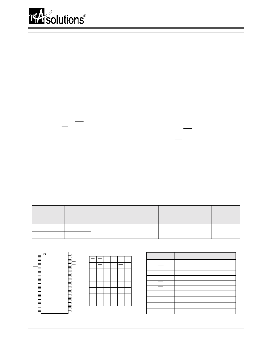
Pin Configuration
Product Family
Part Number
Package
Type
Operating
Temperature
Power
Supply (Vcc)
Speed
Standby
Current (I
SB
),
Max
Operating
Current (Icc),
Max
N02L163WC2AB
48 - BGA
-40
o
C to +85
o
C
2.3V - 3.6V
55ns @ 2.7V
70ns @ 2.3V
20
µ
A
4 mA @ 1MHz
N02L163WC2AT 44 - TSOP II
PIN
ONE
1
2
3
4
5
6
7
8
9
10
11
12
13
14
15
16
17
18
19
20
21
22
A
4
A
3
A
2
A
1
A
0
CE1
I/O
0
I/O
1
I/O
2
I/O
3
VCC
VSS
I/O
4
I/O
5
I/O
6
I/O
7
WE
A
16
A
15
A
14
A
13
A
12
44
43
42
41
40
39
38
37
36
35
34
33
32
31
30
29
28
27
26
25
24
23
A
5
A
6
A
7
OE
UB
LB
I/O
15
I/O
14
I/O
13
I/O
12
VSS
VCC
I/O
11
I/O
10
I/O
9
I/O
8
CE2
A
8
A
9
A
10
A
11
NC
N
0
2L16
3W
C
2
A
TSO
P
1
2
3
4
5
6
A
LB
OE
A
0
A
1
A
2
CE2
B
I/O
8
UB
A
3
A
4
CE1
I/O
0
C
I/O
9
I/O
10
A
5
A
6
I/O
1
I/O
2
D
V
SS
I/O
11
NC
A
7
I/O
3
V
CC
E
V
CC
I/O
12
NC
A
16
I/O
4
V
SS
F
I/O
14
I/O
13
A
14
A
15
I/O
5
I/O
6
G
I/O
15
NC
A
12
A
13
WE
I/O
7
H
NC
A
8
A
9
A
10
A
11
NC
48 Pin BGA (top)
6 x 8 mm
Pin Descriptions
Pin Name
Pin Function
A
0
-A
16
Address Inputs
WE
Write Enable Input
CE1, CE2
Chip Enable Input
OE
Output Enable Input
LB
Lower Byte Enable Input
UB
Upper Byte Enable Input
I/O
0
-I/O
15
Data Inputs/Outputs
V
CC
Power
V
SS
Ground
NC
Not Connected

Stock No. 23140-04 1/02
2
The specifications of this device are subject to change without notice. For latest documentation see http://www.nanoamp.com.
NanoAmp Solutions, Inc.
N02L163WC2A
Functional Block Diagram
Functional Description
CE1
CE2
WE
OE
UB
LB
I/O
0
- I/O
15
1
1. When UB and LB are in select mode (low), I/O
0
- I/O
15
are affected as shown. When LB only is in the select mode only I/O
0
- I/O
7
are affected as shown. When UB is in the select mode only I/O
8
- I/O
15
are affected as shown.
MODE
POWER
H
X
X
X
X
X
High Z
Standby
2
2. When the device is in standby mode, control inputs (WE, OE, UB, and LB), address inputs and data input/outputs are internally
isolated from any external influence and disabled from exerting any influence externally.
Standby
X
L
X
X
X
X
High Z
Standby
2
Standby
L
H
X
X
H
H
High Z
Standby
Standby
L
H
L
X
3
3. When WE is invoked, the OE input is internally disabled and has no effect on the circuit.
L
1
L
1
Data In
Write
3
Active
L
H
H
L
L
1
L
1
Data Out
Read
Active
L
H
H
H
L
1
L
1
High Z
Active
Active
Capacitance
1
1. These parameters are verified in device characterization and are not 100% tested
Item
Symbol
Test Condition
Min
Max
Unit
Input Capacitance
C
IN
V
IN
= 0V, f = 1 MHz, T
A
= 25
o
C
8
pF
I/O Capacitance
C
I/O
V
IN
= 0V, f = 1 MHz, T
A
= 25
o
C
8
pF
I/O
8
- I/O
15
Control
Logic
Page
Decode
Logic
Address
Inputs
A
4
- A
16
Input/
Output
Mux
and
Buffers
I/O
0
- I/O
7
Address
Word
Decode
Logic
Address
Address
Inputs
A
0
- A
3
8K Page
x 16 word
x 16 bit
RAM Array
Wo
r
d
M
u
x
CE1
CE2
WE
OE
UB
LB
Wo
r
d
M
u
x
Stock No. 23140-04 1/02
3
The specifications of this device are subject to change without notice. For latest documentation see http://www.nanoamp.com.
NanoAmp Solutions, Inc.
N02L163WC2A
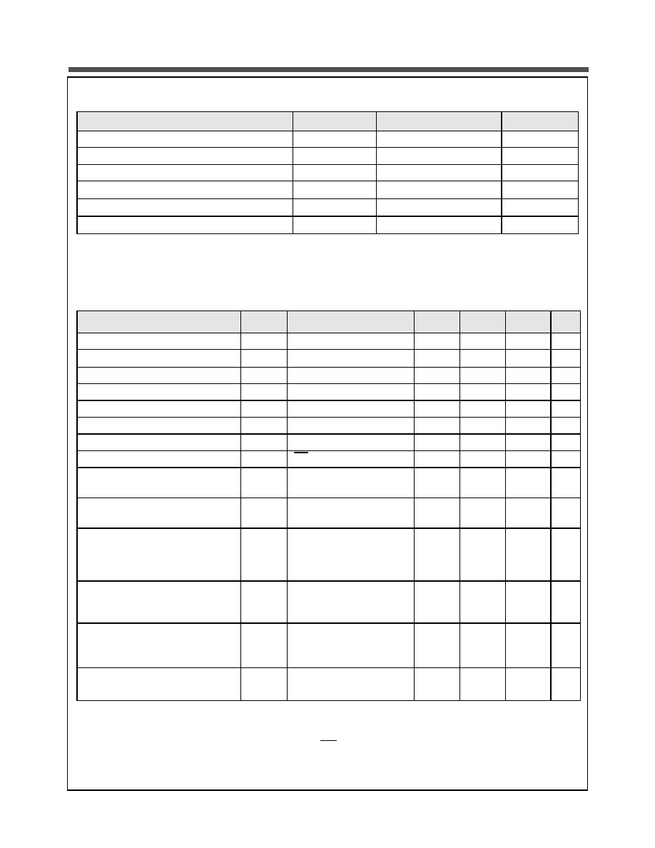
Absolute Maximum Ratings
1
1. Stresses greater than those listed above may cause permanent damage to the device. This is a stress rating only and functional
operation of the device at these or any other conditions above those indicated in the operating section of this specification is not
implied. Exposure to absolute maximum rating conditions for extended periods may affect reliability.
Item
Symbol
Rating
Unit
Voltage on any pin relative to V
SS
V
IN,OUT
≠0.3 to V
CC
+0.3
V
Voltage on V
CC
Supply Relative to V
SS
V
CC
≠0.3 to 4.5
V
Power Dissipation
P
D
500
mW
Storage Temperature
T
STG
≠40 to 125
o
C
Operating Temperature
T
A
-40 to +85
o
C
Soldering Temperature and Time
T
SOLDER
240
o
C, 10sec(Lead only)
o
C
Operating Characteristics (Over Specified Temperature Range)
Item
Symbol
Test Conditions
Min.
Typ
1
1. Typical values are measured at Vcc=Vcc Typ., T
A
=25∞C and not 100% tested.
Max
Unit
Supply Voltage
V
CC
2.3
3.0
3.6
V
Data Retention Voltage
V
DR
Chip Disabled
3
1.8
3.6
V
Input High Voltage
V
IH
1.8
V
CC
+0.3
V
Input Low Voltage
V
IL
≠0.3
0.6
V
Output High Voltage
V
OH
I
OH
= 0.2mA
V
CC
≠0.2
V
Output Low Voltage
V
OL
I
OL
= -0.2mA
0.2
V
Input Leakage Current
I
LI
V
IN
= 0 to V
CC
0.5
µ
A
Output Leakage Current
I
LO
OE = V
IH
or Chip Disabled
0.5
µ
A
Read/Write Operating Supply Current
@ 1
µ
s Cycle Time
2
2. This parameter is specified with the outputs disabled to avoid external loading effects. The user must add current required to drive
output capacitance expected in the actual system.
I
CC1
VCC=3.6 V, V
IN
=V
IH
or V
IL
Chip Enabled, I
OUT
= 0
2.0
4.0
mA
Read/Write Operating Supply Current
@ 70 ns Cycle Time
2
I
CC2
VCC=3.6 V, V
IN
=V
IH
or V
IL
Chip Enabled, I
OUT
= 0
12.0
16.0
mA
Page Mode Operating Supply Current
@ 70ns Cycle Time
2
(Refer to Power
Savings with Page Mode Operation
diagram)
I
CC3
VCC=3.6 V, V
IN
=V
IH
or V
IL
Chip Enabled, I
OUT
= 0
4.0
mA
Read/Write Quiescent Operating Sup-
ply Current
3
3. This device assumes a standby mode if the chip is disabled (CE1 high or CE2 low). In order to achieve low standby current all
inputs must be within 0.2 volts of either VCC or VSS.
I
CC4
V
CC
=3.6 V, V
IN
=V
IH
or V
IL
Chip Enabled, I
OUT
= 0,
f = 0
3.0
mA
Maximum Standby Current
3
I
SB1
V
IN
= V
CC
or 0V
Chip Disabled
t
A
= 85
o
C, VCC = 3.6 V
2.0
20.0
µ
A
Maximum Data Retention Current
3
I
DR
Vcc = 1.8V, V
IN
= V
CC
or 0
Chip Disabled, t
A
= 85
o
C
10.0
µ
A

Stock No. 23140-04 1/02
4
The specifications of this device are subject to change without notice. For latest documentation see http://www.nanoamp.com.
NanoAmp Solutions, Inc.
N02L163WC2A
Power Savings with Page Mode Operation (WE = V
IH
)
Note: Page mode operation is a method of addressing the SRAM to save operating current. The internal
organization of the SRAM is optimized to allow this unique operating mode to be used as a valuable power
saving feature.
The only thing that needs to be done is to address the SRAM in a manner that the internal page is left open
and 16-bit words of data are read from the open page. By treating addresses A0-A3 as the least significant
bits and addressing the 16 words within the open page, power is reduced to the page mode value which is
considerably lower than standard operating currents for low power SRAMs.
Page Address (A4 - A16)
LB, UB
OE
CE1
CE2
Word Address (A0 - A3)
Open page
Word 1
Word 2
Word 16
...

Stock No. 23140-04 1/02
5
The specifications of this device are subject to change without notice. For latest documentation see http://www.nanoamp.com.
NanoAmp Solutions, Inc.
N02L163WC2A
Timing Test Conditions
Item
Input Pulse Level
0.1V
CC
to 0.9 V
CC
Input Rise and Fall Time
5ns
Input and Output Timing Reference Levels
0.5 V
CC
Output Load
CL = 30pF
Operating Temperature
-40 to +85
o
C
Timing
Item
Symbol
2.3 - 3.6 V
2.7 - 3.6 V
Units
Min.
Max.
Min.
Max.
Read Cycle Time
t
RC
70
55
ns
Address Access Time
t
AA
70
55
ns
Chip Enable to Valid Output
t
CO
70
55
ns
Output Enable to Valid Output
t
OE
35
30
ns
Byte Select to Valid Output
t
LB
, t
UB
70
55
ns
Chip Enable to Low-Z output
t
LZ
10
10
ns
Output Enable to Low-Z Output
t
OLZ
5
5
ns
Byte Select to Low-Z Output
t
LBZ
, t
UBZ
10
10
ns
Chip Disable to High-Z Output
t
HZ
0
20
0
20
ns
Output Disable to High-Z Output
t
OHZ
0
20
0
20
ns
Byte Select Disable to High-Z Output
t
LBHZ
, t
UBHZ
0
20
0
20
ns
Output Hold from Address Change
t
OH
10
10
ns
Write Cycle Time
t
WC
70
55
ns
Chip Enable to End of Write
t
CW
50
40
ns
Address Valid to End of Write
t
AW
50
40
ns
Byte Select to End of Write
t
LBW
, t
UBW
50
40
ns
Write Pulse Width
t
WP
40
40
ns
Address Setup Time
t
AS
0
0
ns
Write Recovery Time
t
WR
0
0
ns
Write to High-Z Output
t
WHZ
20
20
ns
Data to Write Time Overlap
t
DW
40
35
ns
Data Hold from Write Time
t
DH
0
0
ns
End Write to Low-Z Output
t
OW
10
10
ns

Stock No. 23140-04 1/02
6
The specifications of this device are subject to change without notice. For latest documentation see http://www.nanoamp.com.
NanoAmp Solutions, Inc.
N02L163WC2A
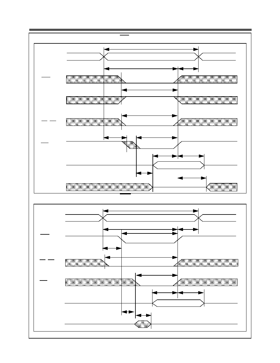
Timing of Read Cycle (CE1 = OE = V
IL
, WE = CE2 = V
IH
)
Timing Waveform of Read Cycle (WE=V
IH
)
Address
Data Out
t
RC
t
AA
t
OH
Data Valid
Previous Data Valid
Address
LB, UB
OE
Data Valid
t
RC
t
AA
t
CO
t
HZ
t
OHZ
t
LBHZ,
t
UBHZ
t
OLZ
t
OE
t
LZ
High-Z
Data Out
t
LB,
t
UB
t
LBLZ,
t
UBLZ
CE1
CE2
Stock No. 23140-04 1/02
7
The specifications of this device are subject to change without notice. For latest documentation see http://www.nanoamp.com.
NanoAmp Solutions, Inc.
N02L163WC2A
Timing Waveform of Write Cycle (WE control)
Timing Waveform of Write Cycle (CE1 Control)
Address
Data In
CE1
CE2
LB, UB
Data Valid
t
WC
t
AW
t
CW
t
WR
t
WHZ
t
DH
High-Z
WE
Data Out
High-Z
t
OW
t
AS
t
WP
t
DW
t
LBW
, t
UBW
Address
WE
Data Valid
t
WC
t
AW
t
CW
t
WR
t
DH
LB, UB
Data In
High-Z
t
AS
t
WP
t
LZ
t
DW
t
LBW
, t
UBW
Data Out
t
WHZ
CE1
(for CE2 Control, use
inverted signal)
Stock No. 23140-04 1/02
8
The specifications of this device are subject to change without notice. For latest documentation see http://www.nanoamp.com.
NanoAmp Solutions, Inc.
N02L163WC2A
44-Lead TSOP II Package (T44)
Note:
1. All dimensions in inches (Millimeters)
2. Package dimensions exclude molding flash
18.41±0.13
10.16±0.13
SEE DETAIL B
1.10±0.15
11.76±0.20
0.45
0.30
0.80mm REF
DETAIL B
0.80mm REF
0
o
-8
o
0.20
0.00
Stock No. 23140-04 1/02
9
The specifications of this device are subject to change without notice. For latest documentation see http://www.nanoamp.com.
NanoAmp Solutions, Inc.
N02L163WC2A
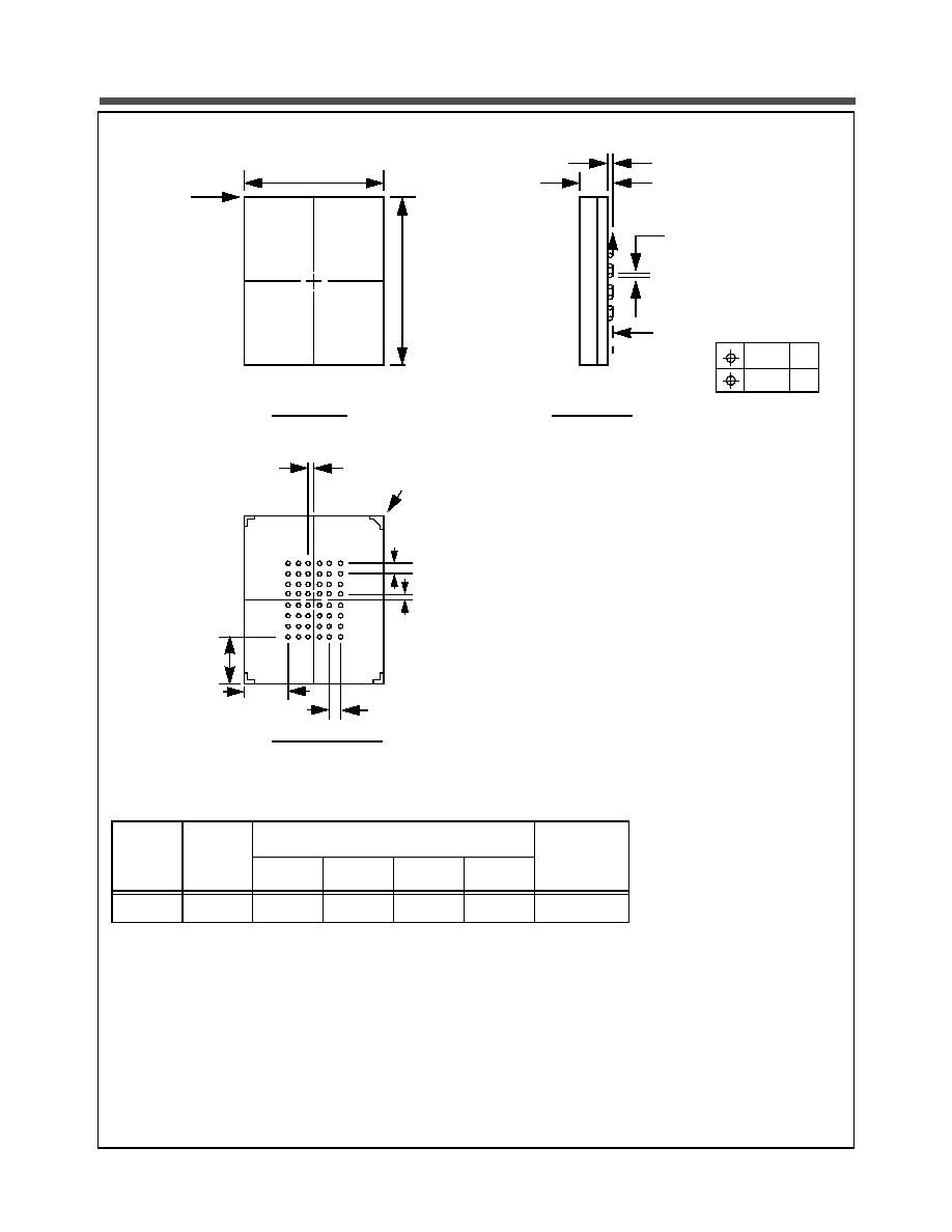
Ball Grid Array Package
Dimensions (mm)
D
E
e = 0.75
BALL
MATRIX
TYPE
SD
SE
J
K
6±0.10
8±0.10
0.375
0.375
1.125
1.375
FULL
SIDE VIEW
TOP VIEW
BOTTOM VIEW
E
D
A1 BALL PAD
CORNER (3)
1.24±0.10
0.28±0.05
0.15
0.05
Z
Z
1. 0.35±0.05 DIA.
1. DIMENSION IS MEASURED AT THE
MAXIMUM SOLDER BALL DIAMETER.
PARALLEL TO PRIMARY Z.
2. PRIMARY DATUM Z AND SEATING
PLANE ARE DEFINED BY THE
SPHERICAL CROWNS OF THE
SOLDER BALLS.
3. A1 BALL PAD CORNER I.D. TO BE
MARKED BY INK.
2. SEATING PLANE - Z
SD
SE
e
K TYP
J TYP
e
A1 BALL PAD
CORNER
Stock No. 23140-04 1/02
10
The specifications of this device are subject to change without notice. For latest documentation see http://www.nanoamp.com.
NanoAmp Solutions, Inc.
N02L163WC2A
Ordering Information
© 2001 - 2002 Nanoamp Solutions, Inc. All rights reserved.
NanoAmp Solutions, Inc. ("NanoAmp") reserves the right to change or modify the information contained in this data sheet and the products described therein, without prior notice.
NanoAmp does not convey any license under its patent rights nor the rights of others. Charts, drawings and schedules contained in this data sheet are provided for illustration pur-
poses only and they vary depending upon specific applications.
NanoAmp makes no warranty or guarantee regarding suitability of these products for any particular purpose, nor does NanoAmp assume any liability arising out of the application
or use of any product or circuit described herein. NanoAmp does not authorize use of its products as critical components in any application in which the failure of the NanoAmp
product may be expected to result in significant injury or death, including life support systems and critical medical instruments.
Revision History
Revision
Date
Change Description
01
Jan. 2001
Initial Preliminary Release
02
May 2001
Changed access time to 55 ns
03
Sept. 2001
Minor parametric modifications. Full production release.
04
Dec. 2001
Part number change from EM128J16, modified Overview and Features, added
Page Mode Operation diagram, revised Operating Characteristics table, Package
diagram, Functional Description table and Ordering Information diagram
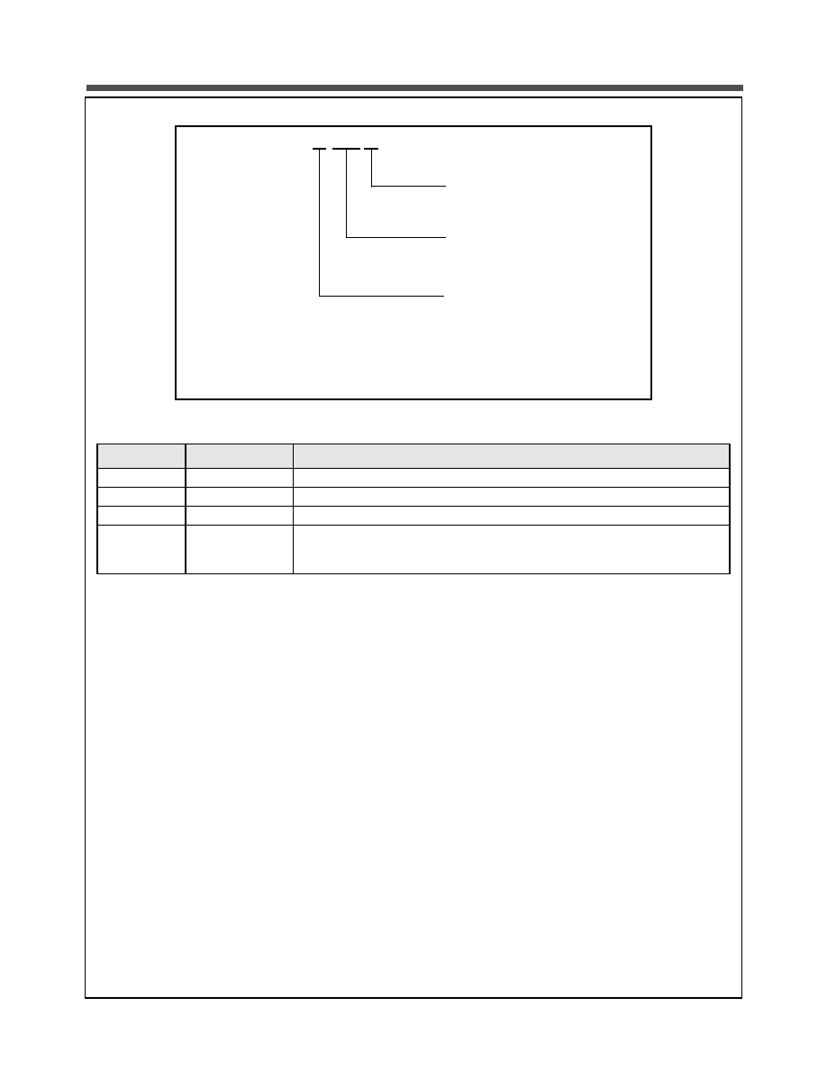
N02L163WC2AX-XX X
I = Industrial, -40∞C to 85∞C
55 = 55ns
T = 44-pin TSOP II
B = 48-ball BGA
Temperature
Performance
Package Type
Note: Add -T&R following the part number for Tape and Reel. Orders will be
considered in tray if not noted.