NanoAmp Solutions, Inc.
670 North McCarthy Blvd. Suite 220, Milpitas, CA 95035
ph: 408-935-7777, FAX: 408-935-7770
www.nanoamp.com
(DOC#14-02-036 Rev C ECN#01-0887)
1
The specifications of this device are subject to change without notice. For latest documentation see http://www.nanoamp.com.
N02M0818L2A
2Mb Ultra-Low Power Asynchronous Medical CMOS SRAM
256Kx8 bit
Overview
The N02M0818L2A is an integrated memory
device intended for implanted life-support (Class 3)
medical applications. This device comprises a 2
Mbit Static Random Access Memory organized as
262,144 words by 8 bits. The device is designed
and fabricated using NanoAmp's advanced CMOS
technology with reliability inhancements for
medical users. The base design is the same as
NanoAmp's N02M0818L1A, which is intended for
non life-support (Class 1 and 2) medical
applications. The device operates with two chip
enable (CE1 and CE2) controls and output enable
(OE) to allow for easy memory expansion. The
N02M0818L2A is optimal for various applications
where low-power is critical such as implanted
pacemaker devices. The device can operate over a
very wide temperature range of -20
o
C to +60
o
C
and is available in die form as well as in JEDEC
standard packages compatible with other standard
256Kb x 8 SRAMs
Features
∑ Single Wide Power Supply Range
1.3 to 2.3 Volts
∑ Very low standby current
200nA typical at 2.1V and 37 deg C
∑ Very low operating current
1 mA at 2.0V and 1µs (Typical)
∑ Very low Page Mode operating current
0.5mA at 1.0V and 1µs (Typical)
∑ Simple memory control
Dual Chip Enables (CE1 and CE2)
Output Enable (OE) for memory expansion
∑ Low voltage data retention
Vcc = 1.0V
∑ Automatic power down to standby mode
∑ TTL compatible three-state output driver
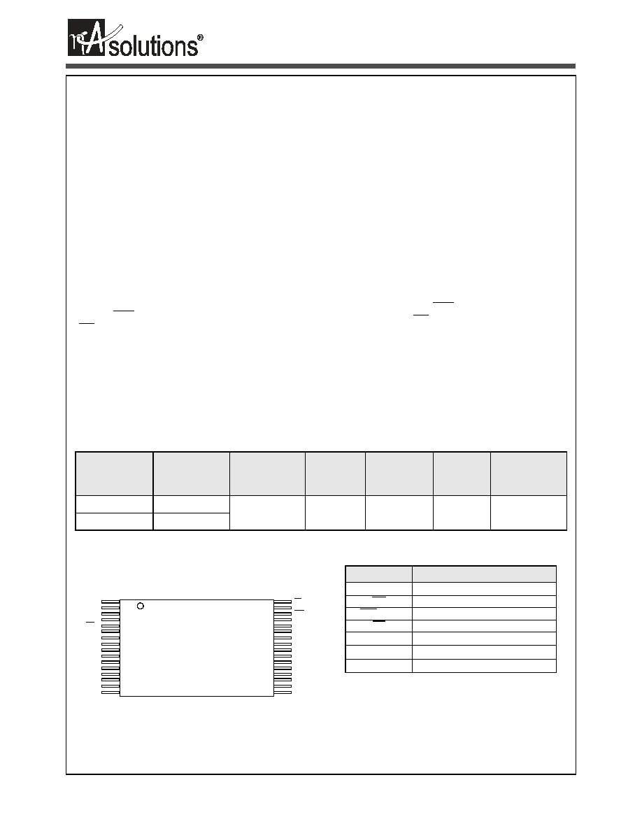
Pin Configuration
Product Family
Part Number
Package Type
Operating
Temperature
Power
Supply (Vcc)
Speed
Standby
Current
(I
SB
)
Operating
Current (Icc),
Max
N02M0818L2AN
32 - STSOP I
-20
o
C to +60
o
C
1.3V - 2.3V
100ns @ 1.65V
500ns @ 1.3V
450nA @
2.3V
2.5 mA @ 1MHz
N02M0818L2AD Known Good Die
A11
A9
A8
A13
WE
CE2
A15
Vcc
A17
A16
A14
A12
A7
A6
A5
A4
1
2
3
4
5
6
7
8
9
10
11
12
13
14
15
16
32
31
30
29
28
27
26
25
24
23
22
21
20
19
18
17
OE
A10
CE1
I/O7
I/O6
I/O5
I/O4
I/O3
Vss
I/O2
I/O1
I/O0
A0
A1
A2
A3
N02M0818L2A
STSOP
Pin Descriptions
Pin Name
Pin Function
A
0
-A
17
Address Inputs
WE
Write Enable Input
CE1, CE2
Chip Enable Input
OE
Output Enable Input
I/O
0
-I/O
7
Data Inputs/Outputs
V
CC
Power
V
SS
Ground
(DOC#14-02-036 Rev C ECN#01-0887)
2
The specifications of this device are subject to change without notice. For latest documentation see http://www.nanoamp.com.
NanoAmp Solutions, Inc.
N02M0818L2A
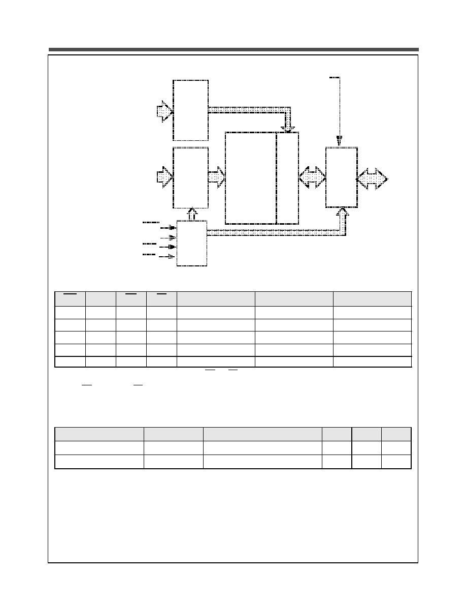
Functional Block Diagram
Functional Description
CE1
CE2
WE
OE
I/O
0
- I/O
7
MODE
POWER
H
X
X
X
High Z
Standby
1
1. When the device is in standby mode, control inputs (WE and OE), address inputs and data input/outputs are internally isolated
from any external influence and disabled from exerting any influence externally.
Standby
X
L
X
X
High Z
Standby
1
Standby
L
H
L
X
2
2. When WE is invoked, the OE input is internally disabled and has no effect on the circuit.
Data In
Write
2
Active
L
H
H
L
Data Out
Read
Active
L
H
H
H
High Z
Active
Active
Capacitance
1
1. These parameters are verified in device characterization and are not 100% tested
Item
Symbol
Test Condition
Min
Max
Unit
Input Capacitance
C
IN
V
IN
= 0V, f = 1 MHz, T
A
= 25
o
C
8
pF
I/O Capacitance
C
I/O
V
IN
= 0V, f = 1 MHz, T
A
= 25
o
C
8
pF
Control
Logic
Page
Decode
Logic
Address
Inputs
A
4
- A
17
Input/
Output
Mux
and
Buffers
I/O
0
- I/O
7
Address
Word
Decode
Logic
Address
Address
Inputs
A
0
- A
3
16K Page
x 16 word
x 8 bit
RAM
Wo
r
d
M
u
x
CE1
CE2
WE
OE
V
CCQ (opt)
(DOC#14-02-036 Rev C ECN#01-0887)
3
The specifications of this device are subject to change without notice. For latest documentation see http://www.nanoamp.com.
NanoAmp Solutions, Inc.
N02M0818L2A
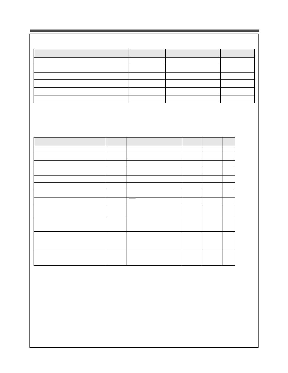
Absolute Maximum Ratings
1
1. Stresses greater than those listed above may cause permanent damage to the device. This is a stress rating only and functional
operation of the device at these or any other conditions above those indicated in the operating section of this specification is not
implied. Exposure to absolute maximum rating conditions for extended periods may affect reliability.
Item
Symbol
Rating
Unit
Voltage on any pin relative to V
SS
V
IN,OUT
≠0.3 to V
CC
+0.3
V
Voltage on V
CC
Supply Relative to V
SS
V
CC
≠0.3 to 3.0
V
Power Dissipation
P
D
500
mW
Storage Temperature
T
STG
≠40 to 125
o
C
Operating Temperature
T
A
-20 to +60
o
C
Soldering Temperature and Time
T
SOLDER
240
o
C, 10sec(Lead only)
o
C
Recommended Operating Limits
(Not all inclusive values tested)1
1. These limits are the expected operating conditions for this device. Only selected points within this range of conditions
are specifically tested and guaranteed.
Item
Symbol
Test Conditions
Min.
Max
Unit
Core Supply Voltage
V
CC
1.3
2.3
V
Data Retention Voltage
V
DR
Chip Disabled (Note 3)
1.0
V
Input High Voltage
V
IH
0.7V
CCQ
V
CCQ
+0.5
V
Input Low Voltage
V
IL
≠0.5
0.3V
CCQ
V
Output High Voltage
V
OH
I
OH
= 0.2mA
V
CCQ
≠0.3
V
Output Low Voltage
V
OL
I
OL
= -0.2mA
0.3
V
Input Leakage Current
I
LI
V
IN
= 0 to V
CC
0.1
µA
Output Leakage Current
I
LO
OE = V
IH
or Chip Disabled
0.1
µA
Read/Write Operating Supply Current
@ 1
µs Cycle Time
2
2. This parameter is specified with the outputs disabled to avoid external loading effects. The user must add current
required to drive output capacitance expected in the actual system.
I
CC1
V
CC
=2.3 V, V
IN
=V
IH
or V
IL
Chip Enabled, I
OUT
= 0
2.5
mA
Read/Write Operating Supply Current
@ 85 ns Cycle Time
2
I
CC2
V
CC
=2.3 V, V
IN
=V
IH
or V
IL
Chip Enabled, I
OUT
= 0
13.0
mA
Standby Current
3
3. The chip is Disabled when CE1# is high or CE2 is low or UB# and LB# are high. The chip is Enabled when CE1# is
low and CE2 is high.
I
SB1
V
IN
= V
CC
or 0V
Chip Disabled
t
A
= 37
o
C, V
CC
= 2.3 V
450
nA
Data Retention Current
3
I
DR
V
CC
= 1.0V, V
IN
= V
CC
or 0
Chip Disabled, t
A
= 85
o
C
1.0
µA
(DOC#14-02-036 Rev C ECN#01-0887)
4
The specifications of this device are subject to change without notice. For latest documentation see http://www.nanoamp.com.
NanoAmp Solutions, Inc.
N02M0818L2A
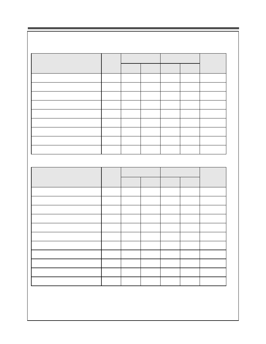
Recommended Timing Limits - Read Cycle
(Not all inclusive values tested)
Item
Symbol
1.3 - 2.3 V
1.65 - 2.3 V
Units
Min.
Max.
Min.
Max.
Read Cycle Time
t
RC
500
100
ns
Address Access Time
t
AA
500
100
ns
Chip Enable to Valid Output
t
CO
500
100
ns
Output Enable to Valid Output
t
OE
200
50
ns
Chip Enable to Low-Z output
t
LZ
100
20
ns
Output Enable to Low-Z Output
t
OLZ
50
10
ns
Chip Disable to High-Z Output
t
HZ
0
150
0
30
ns
Output Disable to High-Z Output
t
OHZ
0
150
0
30
ns
Output Hold from Address Change
t
OH
50
10
ns
Recommended Timing Limits - Write Cycle
(Not all inclusive values tested)
Item
Symbol
1.3 - 2.3 V
1.65 - 2.3 V
Units
Min.
Max.
Min.
Max.
Write Cycle Time
t
WC
500
85
ns
Chip Enable to End of Write
t
CW
400
50
ns
Address Valid to End of Write
t
AW
400
50
ns
Address Setup Time
t
WP
300
40
ns
Write Pulse Width
t
AS
0
0
ns
Write Recovery Time
t
WR
0
0
ns
Write to High-Z Output
t
WHZ
50
15
ns
Data to Write Time Overlap
t
DW
300
40
ns
Data Hold from Write Time
t
DH
0
0
ns
End Write to Low-Z Output
t
OW
50
10
ns
Output Hold from Address Change
t
OH
0
0
ns
(DOC#14-02-036 Rev C ECN#01-0887)
5
The specifications of this device are subject to change without notice. For latest documentation see http://www.nanoamp.com.
NanoAmp Solutions, Inc.
N02M0818L2A
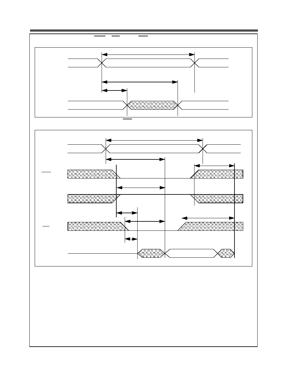
Timing of Read Cycle (CE1 = OE = V
IL
, WE = CE2 = V
IH
)
Timing Waveform of Read Cycle (WE=V
IH
)
Address
Data Out
t
RC
t
AA
t
OH
Data Valid
Previous Data Valid
Address
OE
Data Valid
t
RC
t
AA
t
CO
t
HZ
t
OHZ
t
OLZ
t
OE
t
LZ
High-Z
Data Out
CE1
CE2
(DOC#14-02-036 Rev C ECN#01-0887)
6
The specifications of this device are subject to change without notice. For latest documentation see http://www.nanoamp.com.
NanoAmp Solutions, Inc.
N02M0818L2A
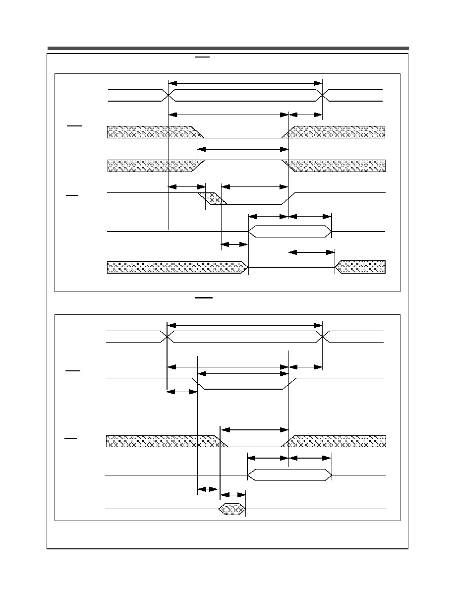
Timing Waveform of Write Cycle (WE control)
Timing Waveform of Write Cycle (CE1 Control)
Address
Data In
CE1
CE2
Data Valid
t
WC
t
AW
t
CW
t
WR
t
WHZ
t
DH
High-Z
WE
Data Out
High-Z
t
OW
t
AS
t
WP
t
DW
Address
WE
Data Valid
t
WC
t
AW
t
CW
t
WR
t
DH
Data In
High-Z
t
AS
t
WP
t
LZ
t
DW
Data Out
t
WHZ
CE1
(for CE2 Control, use
inverted signal)

(DOC#14-02-036 Rev C ECN#01-0887)
7
The specifications of this device are subject to change without notice. For latest documentation see http://www.nanoamp.com.
NanoAmp Solutions, Inc.
N02M0818L2A
32-Lead STSOP-I Package (N32)
Note:
1. All dimensions in millimeters
2. Package dimensions exclude molding flash
13.40±0.20
8.0±0.10
SEE DETAIL B
1.10±0.15
11.80±0.10
0.27
0.17
0.50mm REF
DETAIL B
0.80mm REF
0
o
-8
o
0.20
0.00
(DOC#14-02-036 Rev C ECN#01-0887)
8
The specifications of this device are subject to change without notice. For latest documentation see http://www.nanoamp.com.
NanoAmp Solutions, Inc.
N02M0818L2A
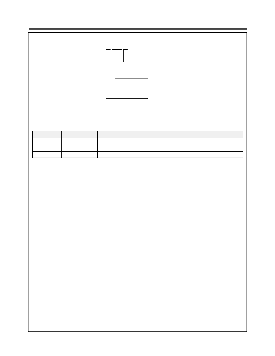
Ordering Information
© 2001 - 2002 Nanoamp Solutions, Inc. All rights reserved.
NanoAmp Solutions, Inc. ("NanoAmp") reserves the right to change or modify the information contained in this data sheet and the products described therein, without prior notice.
NanoAmp does not convey any license under its patent rights nor the rights of others. Charts, drawings and schedules contained in this data sheet are provided for illustration pur-
poses only and they vary depending upon specific applications.
NanoAmp makes no warranty or guarantee regarding suitability of these products for any particular purpose, nor does NanoAmp assume any liability arising out of the application
or use of any product or circuit described herein. NanoAmp does not authorize use of its products as critical components in any application in which the failure of the NanoAmp
product may be expected to result in significant injury or death, including life support systems and critical medical instruments.
Revision History
Revision #
Date
Change Description
A
Dec 2002
Initial Release
B
January 2004
Updated with power characteristics
C
July 2004
General Update
N02M0818L2AX-XX X
20∞C to 60∞C
100 = 100ns @ 1.65V
N = 32-pin STSOP I
D = Known Good Die
Temperature
Performance
Package Type