NanoAmp Solutions, Inc.
670 North McCarthy Blvd. Suite 220, Milpitas, CA 95035
ph: 408-935-7777, FAX: 408-935-7770
www.nanoamp.com
N04Q16yyC2B
Stock No. 23451-B 2/06
1
The specification is ADVANCE INFORMATION and subject to change without notice.
Advance Information
4Mb Ultra-Low Power Asynchronous CMOS SRAM w/ Dual
Vcc and VccQ for Ultimate Power Reduction
256K◊16 bit POWER SAVER TECHNOLOGY
Overview
The N04Q16yyC2B are ultra-low power memory
devices containing a 4 Mbit Static Random Access
Memory organized as 262,144 words by 16 bits.
The device is designed and fabricated using
NanoAmp's advanced CMOS technology to
provide ultra-low active and standby power. The
device operates with two chip enable (CE1 and
CE2) controls and output enable (OE) to allow for
easy memory expansion. Byte controls (UB and
LB) allow the upper and lower bytes to be
accessed independently. The 4Mb SRAM is
optimized for the ultimate in low power and is
suited for various applications where ultra-low-
power is critical such as medical applications,
battery backup and power sensitive hand-held
devices. The unique page mode operation saves
active operating power and the dual power supply
rails allow very low voltage operation while
maintaining 3V I/O capability. The device can
operate over a very wide temperature range of 0
o
C
to +70
o
C for the lowest power and is also available
in the industrial range of -40
o
C to +85
o
C. The
devices are available in standard BGA and TSOP
packages. The devices are also available as
Known Good Die (KGD) for embedded package
applications.
Features
∑ Multiple Power Supply Ranges
1.1V - 1.3V
1.65V - 1.95V
2.3V - 2.7V
2.7V - 3.6V
∑ Dual Vcc / VccQ Power Supplies
1.2V Vcc with 3V VccQ
1.8V Vcc with 3V VccQ
2.5V Vcc with 3V VccQ
∑ Very low standby current
50nA typical for 1.2V operation
∑ Very low operating current
400µA typical for 1.2V operation at 1µs
∑ Very low Page Mode operating current
80µA typical for 1.2V operation at 1µs
∑ Simple memory control
Dual Chip Enables (CE1 and CE2)
Byte control for independent byte operation
Output Enable (OE) for memory expansion
∑ Automatic power down to standby mode
∑ BGA, TSOP and KGD options
∑ RoHS Compliant
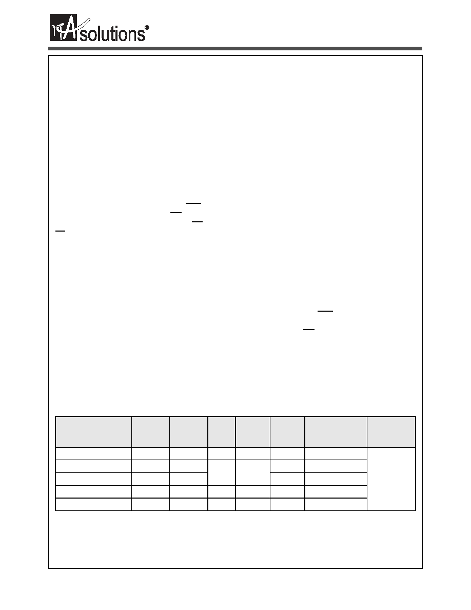
Product Options
Part Number
I/O
Typical
Standby
Current
Vcc
(V)
VccQ
(V)
Speed
(nS)
Typical
Operating Current
Operating
Temperature
N04Q1612C2Bx-15C
x16
50nA
1.2
1.2, 1.8, 3
150ns
0.4 mA @ 1MHz
0
o
C to +70
o
C
N04Q1618C2Bx-15C
x16
50nA
1.8
1.8, 2.5, 3
150ns
0.4 mA @ 1MHz
N04Q1618C2Bx-70C
x16
200nA
70ns
0.6 mA @ 1MHz
N04Q1625C2Bx-15C
x16
800nA
2.5
2.5, 3
150ns
0.6 mA @ 1MHz
N04Q1630C2Bx-70C
x16
800nA
3.0
3.0
70ns
2.2mA @ 1MHz
Stock No. 23451-B 2/06
2
The specification is ADVANCE INFORMATION and subject to change without notice.
NanoAmp Solutions, Inc.
N04Q16yyC2B
Advance Information
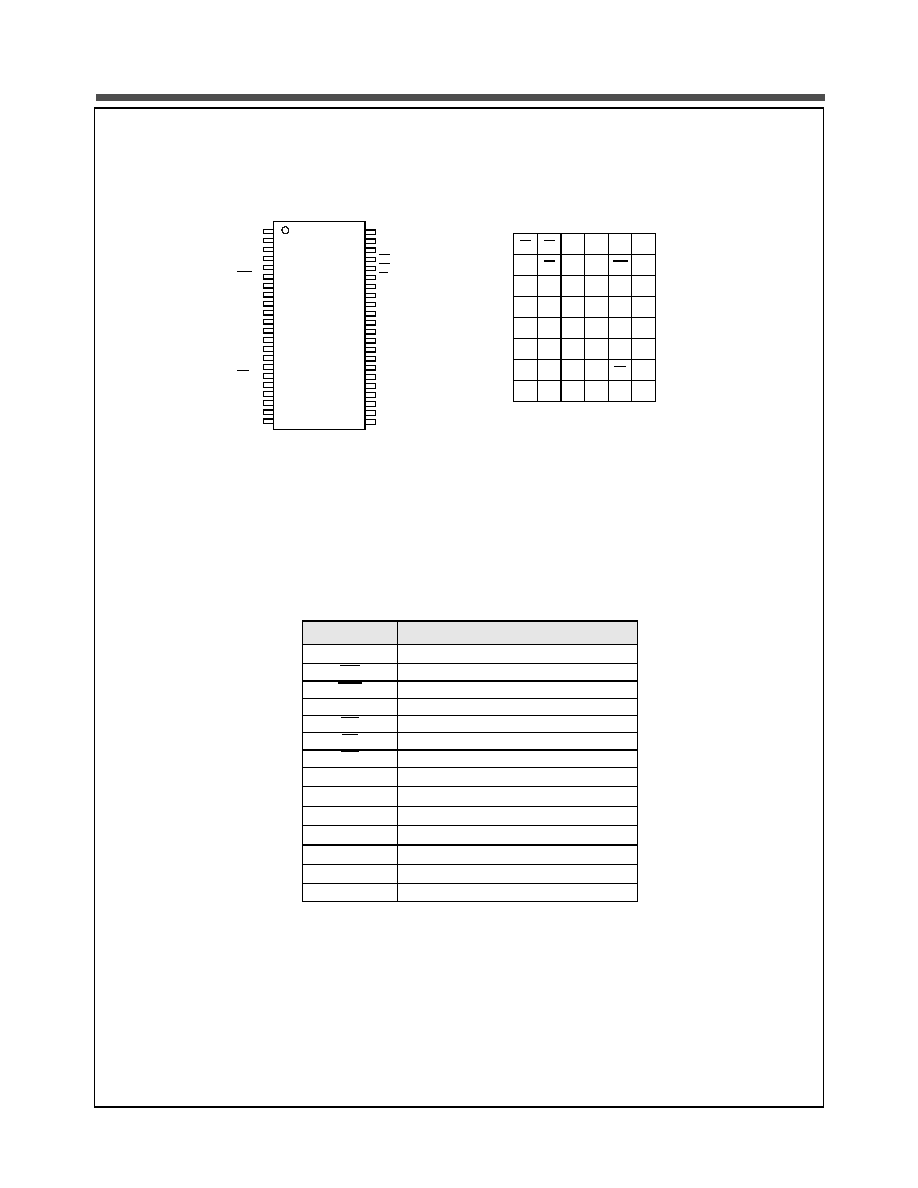
Pin Configurations (4Mb)
Pin Descriptions
Pin Name
Pin Function
A
0
-A
17
Address Inputs
WE
Write Enable Input
CE1
Chip Enable 1 Input
CE2
Chip Enable 2 Input
OE
Output Enable Input
LB
Lower Byte Enable Input
UB
Upper Byte Enable Input
I/O
0
-I/O
7
Lower Byte Data Input/Output
I/O
8
-I/O
15
Upper Byte Data Input/Output
V
CC
Core Power
V
CCQ
Power for I/O
V
SS
Core Ground
V
SSQ
Ground for I/O
NC
Not Connected
PIN
ONE
1
2
3
4
5
6
7
8
9
10
11
12
13
14
15
16
17
18
19
20
21
22
A
4
A
3
A
2
A
1
A
0
CE1
I/O
0
I/O
1
I/O
2
I/O
3
VCCQ
VSSQ
I/O
4
I/O
5
I/O
6
I/O
7
WE
A
16
A
15
A
14
A
13
A
12
44
43
42
41
40
39
38
37
36
35
34
33
32
31
30
29
28
27
26
25
24
23
A
5
A
6
A
7
OE
UB
LB
I/O
15
I/O
14
I/O
13
I/O
12
VSS
VCC
I/O
11
I/O
10
I/O
9
I/O
8
CE2
A
8
A
9
A
10
A
11
A
17
TSOP II
1
2
3
4
5
6
A
LB
OE
A
0
A
1
A
2
CE2
B
I/O
8
UB
A
3
A
4
CE1
I/O
0
C
I/O
9
I/O
10
A
5
A
6
I/O
1
I/O
2
D
V
SSQ
I/O
11
A
17
A
7
I/O
3
V
CC
E
V
CCQ
I/O
12
NC
A
16
I/O
4
V
SS
F
I/O
14
I/O
13
A
14
A
15
I/O
5
I/O
6
G
I/O
15
NC
A
12
A
13
WE
I/O
7
H
NC
A
8
A
9
A
10
A
11
NC
48 Pin BGA (top)
Stock No. 23451-B 2/06
3
The specification is ADVANCE INFORMATION and subject to change without notice.
NanoAmp Solutions, Inc.
N04Q16yyC2B
Advance Information
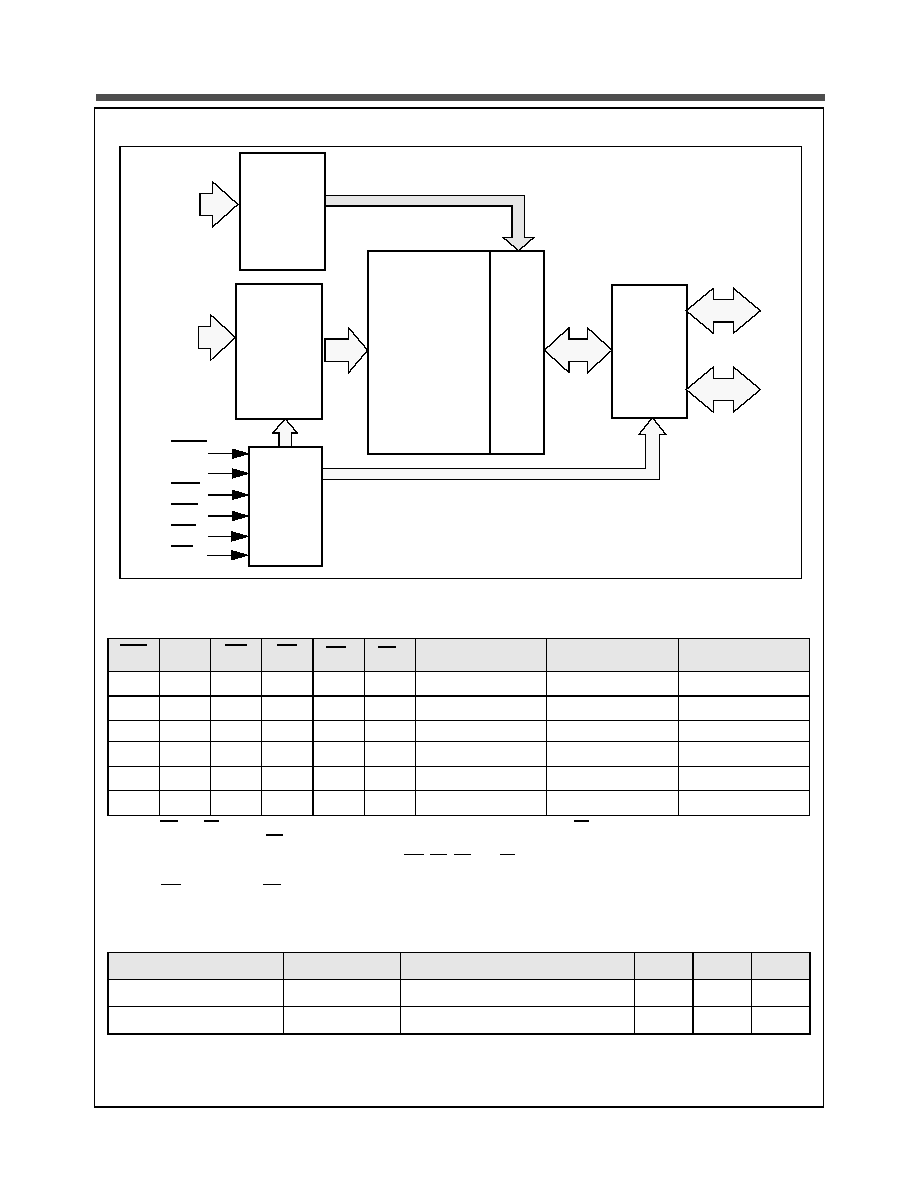
Functional Block Diagram
Functional Description
CE1
CE2
WE
OE
UB
1
LB
1
I/O
0
- I/O
15
1
1. When UB and LB are in select mode (low), I/O
0
- I/O
15
are affected as shown. When LB only is in the select mode only I/O
0
- I/O
7
are affected as shown. When UB is in the select mode only I/O
8
- I/O
15
are affected as shown.
MODE
POWER
H
X
X
X
X
X
High Z
Standby
2
2. When the device is in standby mode, control inputs (WE, OE, UB, and LB), address inputs and data input/outputs are internally
isolated from any external influence and disabled from exerting any influence externally.
Standby
X
L
X
X
X
X
High Z
Standby
2
Standby
L
H
X
X
H
H
High Z
Standby
Standby
L
H
L
X
3
3. When WE is invoked, the OE input is internally disabled and has no effect on the circuit.
L
1
L
1
Data In
Write
3
Active
L
H
H
L
L
1
L
1
Data Out
Read
Active
L
H
H
H
L
1
L
1
High Z
Active
Active
Capacitance
1
1. These parameters are verified in device characterization and are not 100% tested
Item
Symbol
Test Condition
Min
Max
Unit
Input Capacitance
C
IN
V
IN
= 0V, f = 1 MHz, T
A
= 25
o
C
8
pF
I/O Capacitance
C
I/O
V
IN
= 0V, f = 1 MHz, T
A
= 25
o
C
8
pF
Address
Inputs
(A1 - A4)
Address
Inputs
(A0, A5 - A17)
Word
Address
Decode
Logic
4Mb
RAM Array
Wo
r
d
M
u
x
Input/
Output
Mux
and
Buffers
Page
Address
Decode
Logic
Control
Logic
CE1
CE2
WE
OE
UB
LB
I/O0 - I/O7
I/O8 - I/O15
Stock No. 23451-B 2/06
4
The specification is ADVANCE INFORMATION and subject to change without notice.
NanoAmp Solutions, Inc.
N04Q16yyC2B
Advance Information
Absolute Maximum Ratings
1
1. Stresses greater than those listed above may cause permanent damage to the device. This is a stress rating only and functional operation of the
device at these or any other conditions above those indicated in the operating section of this specification is not implied. Exposure to absolute maximum
rating conditions for extended periods may affect reliability.
Item
Symbol
Rating
Unit
Voltage on any pin relative to V
SS
V
IN,OUT
≠0.3 to V
CC
+0.3
V
Voltage on V
CC
Supply Relative to V
SS
V
CC
≠0.3 to 4
V
Power Dissipation
P
D
500
mW
Storage Temperature
T
STG
≠40 to 125
o
C
Operating Temperature
T
A
-40 to +85
o
C
Soldering Temperature and Time
T
SOLDER
260
o
C, 10sec
o
C
Operating Characteristics (Over Specified Temperature Range)
Item
Symbol
Device
Conditions
Min.
Typ
Max
Unit
Core Supply Voltage
V
CC
N04Q1612...
1.2V Core Device
1.1
1.2
1.3
V
N04Q1618...
1.8V Core Device
1.65
1.8
1.95
N04Q1625...
2.5V Core Device
2.3
2.5
2.8
N04Q1630...
3V Core Device
2.7
3.0
3.6
I/O Supply Voltage
V
CCQ
N04Q1612...
1.2V Core Device
1.1
3.3
V
N04Q1618...
1.8V Core Device
1.65
3.3
N04Q1625...
2.5V Core Device
2.3
3.3
N04Q1630...
3V Core Device
2.7
3.6
Input High Voltage
V
IH
0.8 x
VCCQ
V
CC
+0.3
V
Input Low Voltage
V
IL
≠0.3
0.2 x
VCCQ
Output High Voltage
V
OH
I
OH
= -100uA
V
CC
≠0.2
V
Output Low Voltage
V
OL
I
OL
= 100uA
0.2
V
Input Leakage Current
I
LI
V
IN
= 0 to V
CC
0.5
µA
Output Leakage Current
I
LO
OE = V
IH
or Chip
Disabled
0.5
µA
Stock No. 23451-B 2/06
5
The specification is ADVANCE INFORMATION and subject to change without notice.
NanoAmp Solutions, Inc.
N04Q16yyC2B
Advance Information
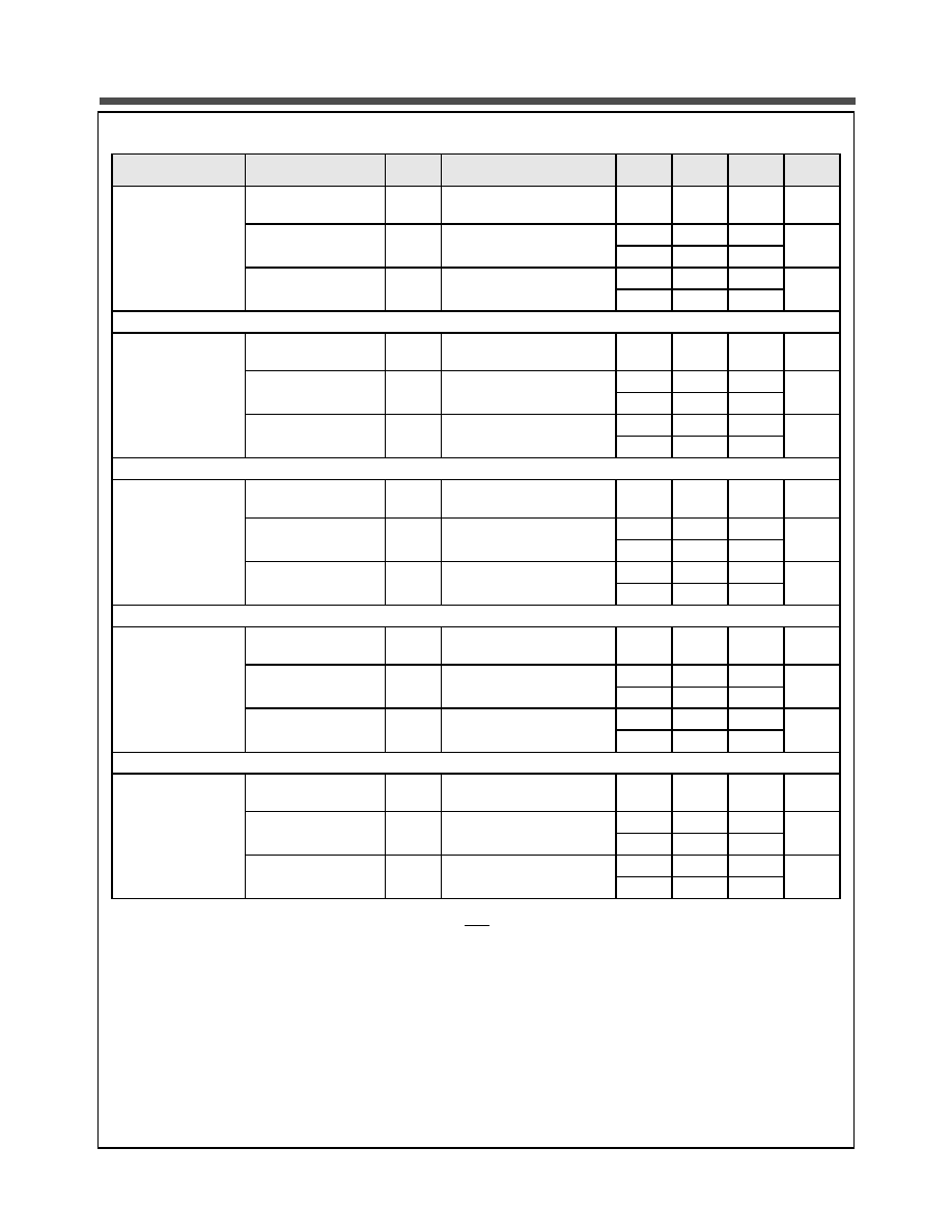
Power Consumption
(T
A
= 0
o
C - 70
o
C)
Device PN
Speed
Typ
1
Max
N04Q1612C2Bx-
15C
Standby Current
2
Isb
Chip Disabled
V
CC
= 1.3V, V
IN
= V
CC
or 0
50
500
nA
Read/Write Current
3
Icc
Chip Enabled, I
OUT
= 0
V
CC
=1.3V, V
IN
=V
IH
or V
IL
1us
0.4
0.5
mA
150ns
2
3
Page Mode Current
Iccp
Chip Enabled, I
OUT
= 0
V
CC
=1.3V, V
IN
=V
IH
or V
IL
1us
80
100
µA
150ns
300
450
N04Q1618C2Bx-
15C
Standby Current
Isb
Chip Disabled
V
CC
= 1.9V, V
IN
= V
CC
or 0V
50
500
nA
Read/Write Current
Icc
Chip Enabled, I
OUT
= 0
V
CC
=1.9V, V
IN
=V
IH
or V
IL
1us
0.4
0.5
mA
150ns
2
3
Page Mode Current
Iccp
Chip Enabled, I
OUT
= 0
V
CC
=1.9V, V
IN
=V
IH
or V
IL
1us
80
100
µA
150ns
400
500
N04Q1618C2Bx-
70C
Standby Current
Isb
Chip Disabled
V
CC
= 1.9V, V
IN
= V
CC
or 0
0.2
1.5
µA
Read/Write Current
Icc
Chip Enabled, I
OUT
= 0
V
CC
=1.9V, V
IN
=V
IH
or V
IL
1us
0.6
0.9
mA
70ns
6
7
Page Mode Current
Iccp
Chip Enabled, I
OUT
= 0
V
CC
=1.9V, V
IN
=V
IH
or V
IL
1us
0.1
0.2
mA
70ns
0.8
1
N04Q1625C2Bx-
15C
Standby Current
Isb
Chip Disabled
V
CC
= 2.8V, V
IN
= V
CC
or 0
0.8
1.0
µA
Read/Write Current
Icc
Chip Enabled, I
OUT
= 0
V
CC
= 2.8V, V
IN
=V
IH
or V
IL
1us
0.6
1.0
mA
150ns
3
4
Page Mode Current
Iccp
Chip Enabled, I
OUT
= 0
V
CC
= 2.8V, V
IN
=V
IH
or V
IL
1us
0.1
0.2
mA
150ns
1.5
2
N04Q1630C2Bx-
70C
Standby Current
Isb
Chip Disabled
V
CC
= 3.6V, V
IN
= V
CC
or 0
0.8
4
µA
Read/Write Current
Icc
Chip Enabled, I
OUT
= 0
V
CC
= 3.6V, V
IN
=V
IH
or V
IL
1us
2.2
3
mA
70ns
8.5
10
Page Mode Current
Iccp
Chip Enabled, I
OUT
= 0
V
CC
= 3.6V, V
IN
=V
IH
or V
IL
1us
0.5
0.6
mA
70ns
2
1.5
1. Typical values are measured at Vcc=Vcc Typ., T
A
=25∞C and not 100% tested.
2. This device assumes a standby mode if the chip is disabled (CE1 high or CE2 low). In order to achieve low standby current all
inputs must be within 0.2 volts of either VCC or VSS. This applies to all ISB values.
3. This parameter is specified with the outputs disabled to avoid external loading effects. The user must add current required to drive
output capacitance expected in the actual system. This applies to all Icc and Iccp values.