- 1 -
4 MEG x 16 ASYNCHRONOUS/PAGE FLASH
52K x 16 SRAM COMBO MEMORY
4 MEG x 16 ASYNCHRONOUS/PAGE FLASH
512K x 16 SRAM COMBO MEMORY
N08C1618E6A
N08C1620E6A
Advance Information
Stock No. 23228-C 03/19/2003
Advance Information Datasheet for N08C16xxE6A
The specifications of this document may change without notice. For the lastest documentation see www.nanoamp.com
NanoAmp Solutions, Inc.
1982 Zanker Road, San Jose, CA 95112
ph: 408-573-8878, FAX: 408-573-8877
www.nanoamp.com
FEATURES
∑ Flexible dual-bank architecture
∑ Support for true concurrent operations with no latency:
Read bank b during program bank a and vice versa
Read bank b during erase bank a and vice versa
∑ Organization:
4,096K x 16 (Flash)
512K x 16 (SRAM)
∑ Basic configuration:
Flash
Bank a (16Mb Flash for data storage)
≠ Eight 4K-word parameter blocks
≠ Thirty-one 32K-word blocks
Bank b (48Mb Flash for program storage)
≠ Ninety-six 32K-word main blocks
SRAM
8Mb SRAM for data storage
≠ 512K-words
∑ F_V
CC
, V
CC
Q, F_V
PP
, S_V
CC
voltages
N08C1620E6A
1.80V (MIN)/2.20V (MAX) F_V
CC
read voltage
1.80V (MIN)/2.20V (MAX) S_V
CC
read voltage
1.80V (MIN)/2.20V (MAX) V
CC
Q
N08C1618E6A
1.70V (MIN)/1.90V (MAX) F_V
CC
read voltage
1.70V (MIN)/1.90V (MAX) S_V
CC
read voltage
1.70V (MIN)/1.90V (MAX) V
CC
Q
Both Parts
1.80V (TYP) F_V
PP
(in-system PROGRAM/ERASE)
1.0V (MIN) S_V
CC
(SRAM data retention)
12V ±5% (HV) F_V
PP
(in-house programming and
accelerated programming algorithm [APA]
activation)
∑ Asynchronous access time
Flash access time: 80ns @ 1.80V F_V
CC
SRAM access time: 80ns @ 1.80V S_V
CC
∑ Page Mode read access
Interpage read access: 80ns @ 1.80V F_V
CC
Intrapage read access: 30ns @ 1.80V F_V
CC
∑ Low power consumption
∑ Enhanced suspend options
ERASE-SUSPEND-to-READ within same bank
PROGRAM-SUSPEND-to-READ within same bank
ERASE-SUSPEND-to-PROGRAM within same bank
∑ Read/Write SRAM during program/erase of Flash
∑ Dual 64-bit chip protection registers for security
purposes (Flash memory)
∑ PROGRAM/ERASE cycles
100,000 WRITE/ERASE cycles per block
∑ Cross-compatible command set support
Extended command set
Common flash interface (CFI) compliant
OPTIONS
MARKING
∑ Timing (also refer to Table 1)
80ns
80
85ns
85
∑ Boot/Parameter Block Location
Top
T
Bottom
B
∑ Operating Temperature Range
Industrial (Extended)
(-40
o
C to +85
o
C)
I
∑ Package
67-ball FBGA (8 x 8 grid)
M3
9mm x 11.5mm x 1.4mm
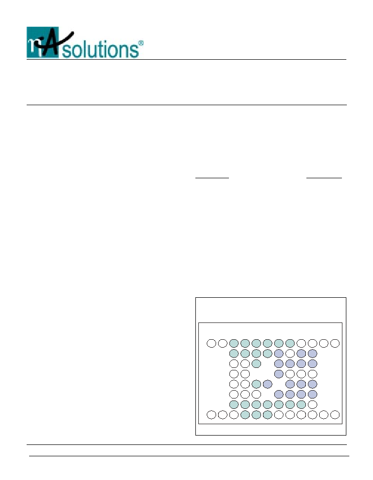
BALL ASSIGNMENT
67-Ball FBGA (Top View)
64x08 Combination Memory Multi-Chip Package (MCP)
64Mb (4Mbx16) Dual Bank Flash Memory plus 8Mb (512Kbx16) SRAM
1.8V, 80ns Access Time, 67-Ball FBGA, Industrial Temperature Range
A
B
C
D
E
F
G
H
1 2 3 4 5 6 7 8 9 10
11
12
Top View
(Ball Down)
NC
NC
A14
A9
DQ11
A6
A0
A15
A10
A21
A19
S_OE#
A7
A4
A20
A16
F_WE#
VSS
F_WP#
S_LB#
A18
F_VCC
A12
S_WE#
DQ6
S_CE2
DQ10
DQ8
A2
F_VSS
F_VSS
DQ14
DQ4
S_VCC
DQ2
DQ0
A1
F_OE#
VccQ
DQ7
DQ5
F_VCC
DQ3
DQ1
S_CE1#
NC
NC
NC
NC
NC
A13
DQ15
DQ13
DQ12
DQ9
A3
F_CE#
NC
NC
A11
A8
NC
F_RP#
F_VPP
S_UB#
A17
A5
4 MEG x 16 ASYNCHRONOUS/PAGE FLASH
512K x 16 SRAM COMBO MEMORY
N08C1618E6A N08C1620E6A
Advance Information
NanoAmp Solutions, Inc.
Stock No. 23228-C 03/19/2003
Advance Information Datasheet for N08C16xxE6A
- 2 -
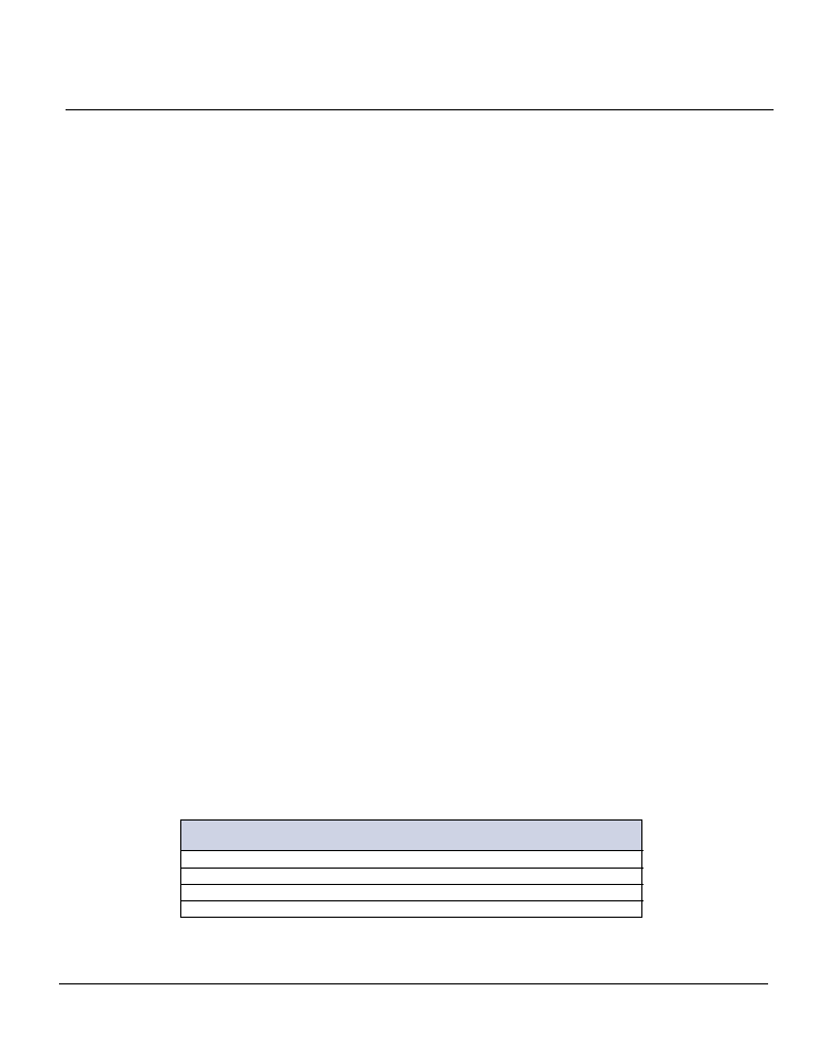
Table 1
Device Markings
PART NUMBER
N08C1620E6AM3-8BI
N08C1620E6AM3-8TI
N08C1618E6AM3-8BI
N08C1618E6AM3-8TI
GENERAL DESCRIPTION
The N08C16xxE6A combination Flash and SRAM
memory devices provide a compact, low-power solution for
systems where printed circuit board real estate is at a
premium. The dual-bank Flash devices are high-perfor-
mance, high-density, nonvolatile memory with a revolution-
ary architecture that can significantly improve system per-
formance.
This new architecture features:
∑ A two-memory-bank configuration supporting dual-
bank operation;
∑ A high-performance bus interface providing a fast page
data transfer; and
∑ A conventional asynchronous bus interface.
The devices also provide soft protection for blocks by
configuring soft protection registers with dedicated com-
mand sequences. For security purposes, dual 64-bit chip
protection registers are provided.
The embedded WORD WRITE and BLOCK ERASE
functions are fully automated by an on-chip write state
machine (WSM). The WSM simplifies these operations and
relieves the system processor of secondary tasks. An on-
chip status register, one for each bank, can be used to
monitor the WSM status to determine the progress of a
PROGRAM/ERASE command.
The erase/program suspend functionality allows com-
patibility with existing EEPROM emulation software pack-
ages.
The devices take advantage of a dedicated power source
for the Flash memory (F_V
CC
) and a dedicated power source
for the SRAM (S_V
CC
), both at 1.70V≠2.20V for optimized
power consumption and improved noise immunity. A dedi-
cated I/O power supply (V
CC
Q) is provided with an extended
range (1.70V≠2.20V), to allow a direct interface to most
common logic controllers and to ensure improved noise
immunity. The separate S_V
CC
pin for the SRAM provides
data retention capability when required. The data retention
S_V
CC
is specified as low as 1.0V. The devices support two
F_V
PP
voltage ranges, an in-circuit voltage of 0.9V≠2.2V and
a production compatibility voltage of 12V ±5%. The 12V ±5%
F_V
PP
2
is supported for a maximum of 100 cycles and 10
cumulative hours.
The N08C16xxE6A devices contain an asynchronous
8Mb SRAM organized as 512K-words by 16 bits. The
devices are fabricated using an advanced CMOS process
and high-speed/ultra-low-power circuit technology, and then
are packaged in a 67-ball FBGA package with 0.80mm
pitch.
ARCHITECTURE AND MEMORY
ORGANIZATION
The Flash devices contain two separate banks of memory
(bank a and bank b) for simultaneous READ and WRITE
operations, which are available in the following bank seg-
mentation configuration:
∑ Bank a comprises one-fourth of the memory and
contains 8 x 4K-word parameter blocks, while the
remainder of bank a is split into 31 x 32K-word blocks.
∑ Bank b represents three-fourths of the memory, is
equally sectored, and contains 96 x 32K-word blocks.
Figures 2 and 3 show the bottom and top memory
organizations.
DEVICE MARKING
Due to the size of the package, the standard part number
is not printed on the top of each device. Instead, an
abbreviated device mark comprised of a five-digit alphanu-
meric code is used. The abbreviated device marks are cross
referenced to the part numbers in Table 1.
4 MEG x 16 ASYNCHRONOUS/PAGE FLASH
512K x 16 SRAM COMBO MEMORY
N08C1618E6A N08C1620E6A
Advance Information
NanoAmp Solutions, Inc.
Stock No. 23228-C 03/19/2003
Advance Information Datasheet for N08C16xxE6A
- 3 -
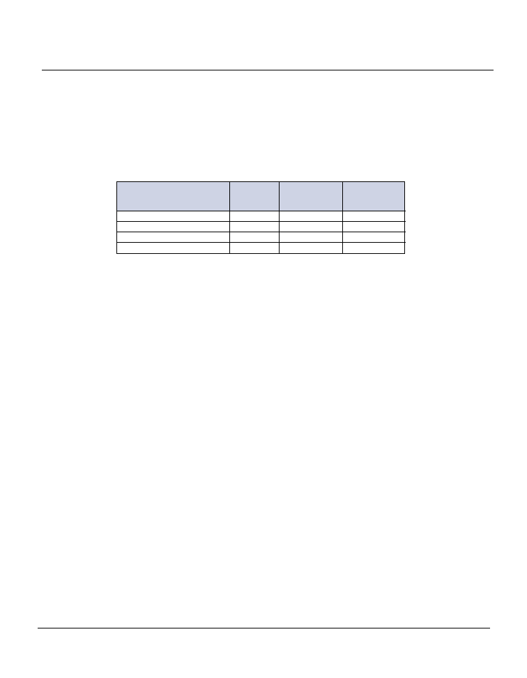
PART NUMBERING INFORMATION
The N08C1618E6A and N08C1620E6A combination
memory MCP products are low-power devices that are
available with several different combinations of features.
Valid combinations of features and their corresponding part
numbers are listed in Table 2.
Table 2
Valid Part Number Combinations
1
BOOT BLOCK
OPERATING
ACCESS
STARTING
TEMPERATURE
PART NUMBER
TIME (ns)
ADDRESS
RANGE
N08C1620E6AM3-8BI
8 0
Bottom
-40
o
C to +85
o
C
N08C1620E6AM3-8TI
8 0
Top
-40
o
C to +85
o
C
N08C1618E6AM3-8BI
8 5
Bottom
-40
o
C to +85
o
C
N08C1618E6AM3-8TI
8 5
Top
-40
o
C to +85
o
C
NOTE: 1. For part numbers or combination memory MCP configurations not
listed in this table, please contact your NanoAmp representative, or
contact NanoAmp directly. Access times vary by core voltage (F_Vcc
and S_Vcc).
4 MEG x 16 ASYNCHRONOUS/PAGE FLASH
512K x 16 SRAM COMBO MEMORY
N08C1618E6A N08C1620E6A
Advance Information
NanoAmp Solutions, Inc.
Stock No. 23228-C 03/19/2003
Advance Information Datasheet for N08C16xxE6A
- 4 -
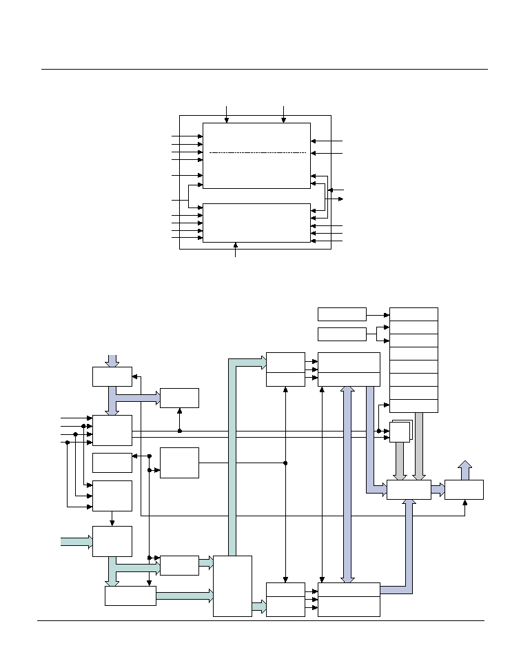
BLOCK DIAGRAM
F_V
PP
S_OE#
S_CE2
S_CE1#
S_WE#
DQ0
≠
DQ15
A19
≠
A20
A0
≠
A18
F_RP#
F_CE#
F_OE#
F_WE#
F_V
CC
F_WP#
F_V
SS
FLASH
SRAM
S_V
SS
S_UB#
S_LB#
4,096K x 16
512K x 16
Bank a
Bank b
S_V
CC
V
CC
Q
FLASH FUNCTIONAL BLOCK DIAGRAM
Address
Input
Buffer
X DEC
Y/Z DEC
Data Input
Buffer
Output
Multiplexer
Address
CNT/WSM
Output
Buffer
Status
Reg.
WSM
Program/
Erase
Pump Voltage
Generators
Address Latch
DQ0-DQ15
DQ0≠DQ15
CSM
F_RST#
F_CE#
X DEC
Y/Z DEC
F_WE#
F_OE#
I/O Logic
A0≠A21
Address
Multiplexer
Bank 2 Blocks
Y/Z Gating/Sensing
Data
Register
Bank 1 Blocks
Y/Z Gating/Sensing
ID Reg.
RCR
Block Lock
Device ID
Manufacturer's ID
OTP
Query
PR Lock
Query/OTP
PR Lock
4 MEG x 16 ASYNCHRONOUS/PAGE FLASH
512K x 16 SRAM COMBO MEMORY
N08C1618E6A N08C1620E6A
Advance Information
NanoAmp Solutions, Inc.
Stock No. 23228-C 03/19/2003
Advance Information Datasheet for N08C16xxE6A
- 5 -
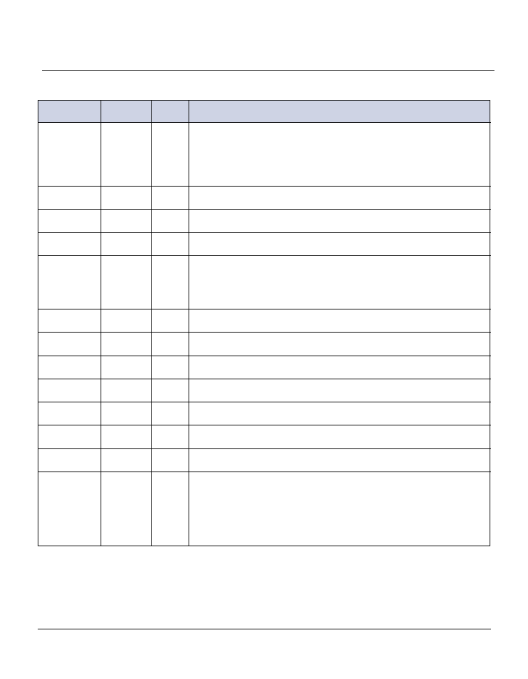
BALL DESCRIPTIONS
67-BALL FBGA
NUMBERS
SYMBOL
TYPE
DESCRIPTION
H6, G9, G8, G7,
A0≠A21
Input
Address Inputs: Inputs for the addresses during READ and WRITE
H5, H4, G6, G5,
operations. Addresses are internally latched during READ and WRITE
B4, B6, B5, A4,
cycles. Flash: A0≠A21; SRAM: A0≠A18.
A8, A7, A6, A5,
B3, G4, G3, E5,
A3, C5
H7
F_CE#
Input
Flash Chip Enable: Activates the device when LOW. When CE# is HIGH, the
device is disabled and goes into standby power mode.
H9
F_OE#
Input
Flash Output Enable: Enables Flash output buffers when LOW. When F_OE# is
HIGH, the output buffers are disabled.
C3
F_WE#
Input
Flash Write Enable: Determines if a given cycle is a Flash WRITE cycle.
F_WE# is active LOW.
D4
F_RP#
Input
Reset. When F_RP# is a logic LOW, the device is in reset, which drives the
outputs to High-Z and resets the WSM. When F_RP# is a logic HIGH, the
device is in standard operation. When F_RP# transitions from logic LOW to logic
HIGH, the device resets all blocks to locked and defaults to the read array
mode.
E3
F_WP#
Input
Flash Write Protect. Controls the lock down function of the flexible locking
feature.
G10
S_CE1#
Input
SRAM Chip Enable1: Activates the SRAM when it is LOW. HIGH level deselects
the SRAM and reduces the power consumption to standby levels.
D8
S_CE2
Input
SRAM Chip Enable2: Activates the SRAM when it is HIGH. LOW level deselects
the SRAM and reduces the power consumption to standby levels.
F5
S_OE#
Input
SRAM Output Enable: Enables SRAM output buffers when LOW. When S_OE#
is HIGH, the output buffers are disabled.
B8
S_WE#
Input
SRAM Write Enable: Determines if a given cycle is an SRAM WRITE cycle.
S_WE# is active LOW.
F3
S_LB#
Input
SRAM Lower Byte: When LOW, it selects the SRAM address lower byte (DQ0≠
DQ7).
F4
S_UB#
Input
SRAM Upper Byte: When LOW, it selects the SRAM address upper byte (DQ8≠
DQ15).
F9, F10, E9,
DQ0≠DQ15
Input/
Data Inputs/Outputs: Input array data on the second CE# and WE#
E10, C9, C10,
Output
cycle during PROGRAM command. Input commands to the command
C8, B10, F8,
user interface when CE# and WE# are active. Output data when CE#
F7, E8, E6, D7,
and OE# are active.
C7, B9, B7
(continued on next page)