NanoAmp Solutions, Inc.
1982 Zanker Road, San Jose, CA 95112
ph: 408-573-8878, FAX: 408-573-8877
www.nanoamp.com
Stock No. 23211-01 11/01/02
1
The specifications of this device are subject to change without notice. For latest documentation see http://www.nanoamp.com.
N08M1618L1A
8Mb Ultra-Low Power Asynchronous Medical CMOS SRAM
512Kx16 bit
Overview
The N08M1618L1A is an integrated memory
device intended for non life-support (Class 1 or
2) medical applications. This device is a 8
megabit memory organized as 524,288 words by
16 bits. The device is designed and fabricated
using NanoAmp's advanced CMOS technology
with reliability inhancements for medical users. The
base design is the same as NanoAmp's
N08M1618L1A, which has further reliability
processing for life-support (Class 3) medical
applications. The device operates with two chip
enable (CE1 and CE2) controls and output enable
(OE) to allow for easy memory expansion. Byte
controls (UB and LB) allow the upper and lower
bytes to be accessed independently and can also
be used to deselect the device. This device is
optimal for various applications where low-power is
critical such as battery backup and hand-held
devices. The device can operate over a very wide
temperature range of -40
o
C to +85
o
C and is
available in a JEDEC standard BGA package.
Features
� Dual voltage for Optimum Performance:
Vccq - 2.3 to 3.6 Volts
Vcc - 1.4 to 2.2 Volts
� Very low standby current
0.4�A at 1.8V and 37 deg C
� Very low operating current
1.0mA at 1.8V and 1�s (Typical)
� Very low Page Mode operating current
0.5mA at 1.8V and 1�s (Typical)
� Simple memory control
Dual Chip Enables (CE1 and CE2)
Byte control for independent byte operation
Output Enable (OE) for memory expansion
� Low voltage data retention
Vcc = 1.2V
� Special Processing to reduce Soft Error Rate
(SER)
� Automatic power down to standby mode
Pin Configuration
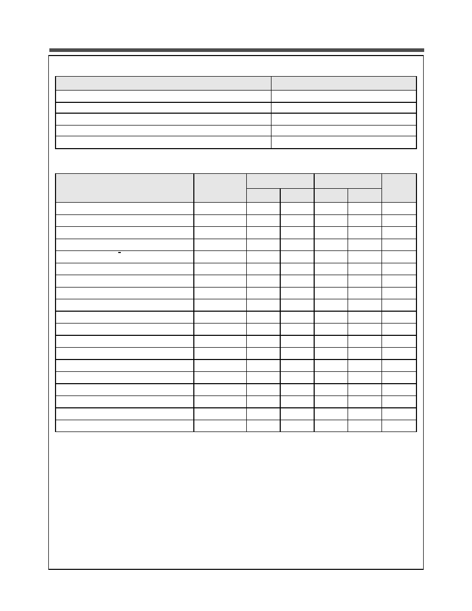
Product Family
Part Number
Package Type
Operating
Temperature
Power
Supply
Speed
Standby
Current (I
SB
),
Max
Operating
Current (Icc),
Max
N08M1618L1AB
48 - BGA
-40
o
C to +85
o
C
1.4V-3.6V(V
CCQ
)
1.4V-2.2V(V
CC
)
85ns @ 1.7V
150ns @ 1.4V
20
�A
3 mA @ 1MHz
N08M1618L1AD Known Good Die
1
2
3
4
5
6
A
LB
OE
A
0
A
1
A
2
CE2
B
I/O
8
UB
A
3
A
4
CE1
I/O
0
C
I/O
9
I/O
10
A
5
A
6
I/O
1
I/O
2
D
V
SS
I/O
11
A
17
A
7
I/O
3
V
CC
E
V
CCQ
I/O
12
NC
A
16
I/O
4
V
SS
F
I/O
14
I/O
13
A
14
A
15
I/O
5
I/O
6
G
I/O
15
NC
A
12
A
13
WE
I/O
7
H
A
18
A
8
A
9
A
10
A
11
NC
48 Pin BGA (top)
8 x 10 mm
Pin Descriptions
Pin Name
Pin Function
A
0
-A
18
Address Inputs
WE
Write Enable Input
CE1, CE2
Chip Enable Input
OE
Output Enable Input
LB
Lower Byte Enable Input
UB
Upper Byte Enable Input
I/O
0
-I/O
15
Data Inputs/Outputs
V
CC
Power
V
SS
Ground
V
CCQ
Power I/O pins only
NC
Not Connected
Stock No. 23211-01 11/01/02
2
The specifications of this device are subject to change without notice. For latest documentation see http://www.nanoamp.com.
NanoAmp Solutions, Inc.
N08M1618L1A
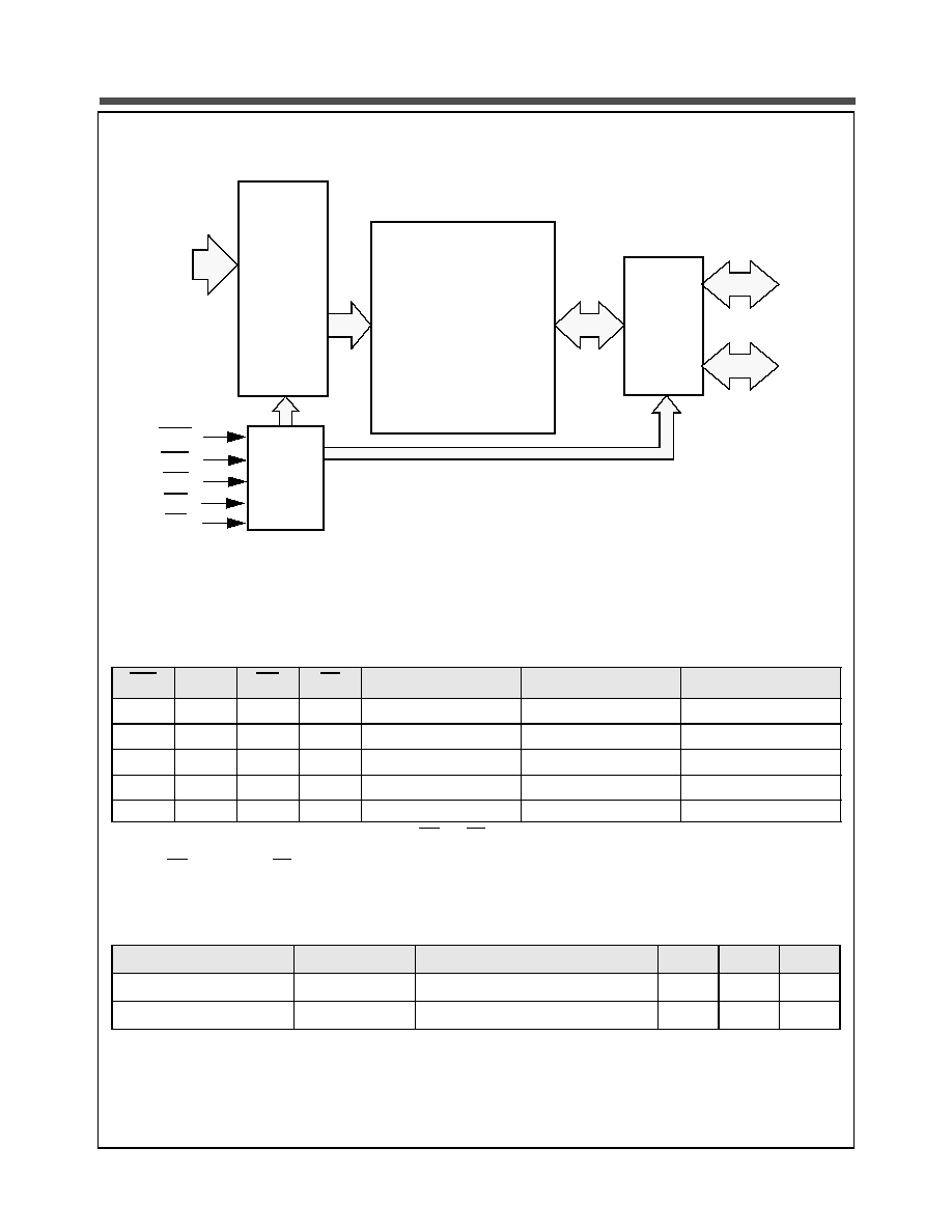
Functional Block Diagram
Functional Description
CE1
CE2
WE
OE
I/O
0
- I/O
7
MODE
POWER
H
X
X
X
High Z
Standby
1
1. When the device is in standby mode, control inputs (WE and OE), address inputs and data input/outputs are internally isolated
from any external influence and disabled from exerting any influence externally.
Standby
X
L
X
X
High Z
Standby
1
Standby
L
H
L
X
2
2. When WE is invoked, the OE input is internally disabled and has no effect on the circuit.
Data In
Write
2
Active
L
H
H
L
Data Out
Read
Active
L
H
H
H
High Z
Active
Active
Capacitance
1
1. These parameters are verified in device characterization and are not 100% tested
Item
Symbol
Test Condition
Min
Max
Unit
Input Capacitance
C
IN
V
IN
= 0V, f = 1 MHz, T
A
= 25
o
C
8
pF
I/O Capacitance
C
I/O
V
IN
= 0V, f = 1 MHz, T
A
= 25
o
C
8
pF
Control
Logic
Decode
Logic
Address
Inputs
A
0
- A
18
WE
OE
Input/
Output
Mux
and
Buffers
I/O
0
- I/O
7
UB
LB
I/O
8
- I/O
15
Address
CE1
512K x 16
Memory
Array
Stock No. 23211-01 11/01/02
3
The specifications of this device are subject to change without notice. For latest documentation see http://www.nanoamp.com.
NanoAmp Solutions, Inc.
N08M1618L1A
Absolute Maximum Ratings
1
1. Stresses greater than those listed above may cause permanent damage to the device. This is a stress rating only and functional
operation of the device at these or any other conditions above those indicated in the operating section of this specification is not
implied. Exposure to absolute maximum rating conditions for extended periods may affect reliability.
Item
Symbol
Rating
Unit
Voltage on any pin relative to V
SS
V
IN,OUT
�0.3 to V
CC
+0.3
V
Voltage on V
CC
Supply Relative to V
SS
V
CC
�0.3 to 4.5
V
Power Dissipation
P
D
500
mW
Storage Temperature
T
STG
�40 to 125
o
C
Operating Temperature
T
A
-40 to +85
o
C
Soldering Temperature and Time
T
SOLDER
240
o
C, 10sec(Lead only)
o
C
Operating Characteristics (Over Specified Temperature Range)
Item
Symbol
Test Conditions
Min.
Typ
1
1. Typical values are measured at Vcc=Vcc Typ., T
A
=25�C and not 100% tested.
Max
Unit
Core Supply Voltage
V
CC
1.4
1.8
2.3
V
I/O Supply Voltage
V
CCQ
V
CCQ
> or = V
CC
1.4
1.8
3.6
V
Data Retention Voltage
V
DR
Chip Disabled
3
1.2
V
Input High Voltage
V
IH
V
CCQ
-0.6
V
CCQ
+0.3
V
Input Low Voltage
V
IL
�0.3
0.6
V
Output High Voltage
V
OH
I
OH
= 0.2mA
V
CCQ
�0.2
V
Output Low Voltage
V
OL
I
OL
= -0.2mA
0.2
V
Input Leakage Current
I
LI
V
IN
= 0 to V
CC
0.1
�A
Output Leakage Current
I
LO
OE = V
IH
or Chip Disabled
0.1
�A
Read/Write Operating Supply Current
@ 1
�s Cycle Time
2
2. This parameter is specified with the outputs disabled to avoid external loading effects. The user must add current required to drive
output capacitance expected in the actual system.
I
CC1
V
CC
=2.3 V, V
IN
=V
IH
or V
IL
Chip Enabled, I
OUT
= 0
1.5
2.5
mA
Read/Write Operating Supply Current
@ 85 ns Cycle Time
2
I
CC2
V
CC
=2.3 V, V
IN
=V
IH
or V
IL
Chip Enabled, I
OUT
= 0
10.0
13.0
mA
Page Mode Operating Supply Current
@ 85 ns Cycle Time
2
(Refer to Power
Savings with Page Mode Operation
diagram)
I
CC3
V
CC
=2.3 V, V
IN
=V
IH
or V
IL
Chip Enabled, I
OUT
= 0
3.5
mA
Read/Write Quiescent Operating Sup-
ply Current
3
3. This device assumes a standby mode if the chip is disabled (CE1 high or CE2 low). In order to achieve low standby current all
inputs must be within 0.2 volts of either VCC or VSS.
I
CC4
V
CC
=2.3 V, V
IN
=V
IH
or V
IL
Chip Enabled, I
OUT
= 0,
f = 0
0.2
�A
Standby Current
3
I
SB1
V
IN
= V
CC
or 0V
Chip Disabled
t
A
= 85
o
C, V
CC
= 2.3 V
0.2
20.0
�A
Data Retention Current
3
I
DR
V
CC
= 1.8V, V
IN
= V
CC
or 0
Chip Disabled, t
A
= 85
o
C
0.1
1.0
�A
Stock No. 23211-01 11/01/02
4
The specifications of this device are subject to change without notice. For latest documentation see http://www.nanoamp.com.
NanoAmp Solutions, Inc.
N08M1618L1A
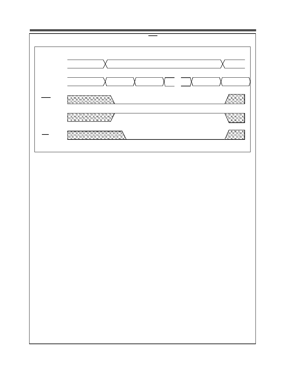
Power Savings with Page Mode Operation (WE = V
IH
)
Note: Page mode operation is a method of addressing the SRAM to save operating current. The internal
organization of the SRAM is optimized to allow this unique operating mode to be used as a valuable power
saving feature.
The only thing that needs to be done is to address the SRAM in a manner that the internal page is left open
and 8-bit words of data are read from the open page. By treating addresses A0-A3 as the least significant
bits and addressing the 16 words within the open page, power is reduced to the page mode value which is
considerably lower than standard operating currents for low power SRAMs.
Page Address (A4 - A17)
OE
CE1
CE2
Word Address (A0 - A3)
Open page
Word 1
Word 2
Word 16
...
Stock No. 23211-01 11/01/02
5
The specifications of this device are subject to change without notice. For latest documentation see http://www.nanoamp.com.
NanoAmp Solutions, Inc.
N08M1618L1A
Timing Test Conditions
Item
Input Pulse Level
0.1V
CC
to 0.9 V
CC
Input Rise and Fall Time
5ns
Input and Output Timing Reference Levels
0.5 V
CC
Output Load
CL = 30pF
Operating Temperature
-40 to +85
o
C
Timing V
CCQ
> or = V
CC
Item
Symbol
V
CC
= 1.4 - 2.3 V
V
CC
= 1.7 - 2.3 V
Units
Min.
Max.
Min.
Max.
Read Cycle Time
t
RC
150
85
ns
Address Access Time
t
AA
150
85
ns
Chip Enable to Valid Output
t
CO
150
85
ns
Output Enable to Valid Output
t
OE
50
40
ns
Chip Enable to Low-Z output
t
LZ
20
10
ns
Output Enable to Low-Z Output
t
OLZ
20
5
ns
Chip Disable to High-Z Output
t
HZ
0
30
0
15
ns
Output Disable to High-Z Output
t
OHZ
0
30
0
15
ns
Output Hold from Address Change
t
OH
20
10
ns
Write Cycle Time
t
WC
150
85
ns
Chip Enable to End of Write
t
CW
75
50
ns
Address Valid to End of Write
t
AW
75
50
ns
Write Pulse Width
t
WP
50
40
ns
Address Setup Time
t
AS
0
0
ns
Write Recovery Time
t
WR
0
0
ns
Write to High-Z Output
t
WHZ
30
15
ns
Data to Write Time Overlap
t
DW
50
40
ns
Data Hold from Write Time
t
DH
0
0
ns
End Write to Low-Z Output
t
OW
10
5
ns