Äîêóìåíòàöèÿ è îïèñàíèÿ www.docs.chipfind.ru
NanoAmp Solutions, Inc.
670 North McCarthy Blvd. Suite 220, Milpitas, CA 95035
ph: 408-935-7777, FAX: 408-935-7770
www.nanoamp.com
N08T1630CxB
(DOC# 14-02-004 REV H ECN# 01-1102)
1
The specifications of this device are subject to change without notice. For latest documentation see http://www.nanoamp.com.
8Mb Ultra-Low Power Asynchronous CMOS SRAM
512Kx16 bit
Overview
The N08T1630CxB is an integrated memory
device containing a low power 8 Mbit SRAM built
using a self-refresh DRAM array organized as
512,288 words by 16 bits. It is designed to be
identical in operation and interface to standard 6T
SRAMS. The device is designed for low standby
and operating current and includes a power-down
feature to automatically enter standby mode. The
device operates with two chip enable (CE1 and
CE2) controls and output enable (OE) to allow for
easy memory expansion. Byte controls (UB and
LB) allow the upper and lower bytes to be
accessed independently and can also be used to
deselect the device. The N08T1630CxB is optimal
for various applications where low-power is critical
such as battery backup and hand-held devices.
The device can operate over a very wide
temperature range of -40
o
C to +85
o
C and is
available in JEDEC standard BGA and TSOP2
packages compatible with other standard 512Kb x
16 SRAMs.
Features
· Single Wide Power Supply Range
2.7 to 3.6 Volts
· Very low standby current
70µA at 3.0V (Max)
· Very low operating current
2.0mA at 3.0V and 1µs (Typical)
· Simple memory control
Dual Chip Enables (CE1 and CE2)
Byte control for independent byte operation
Output Enable (OE) for memory expansion
· Very fast access time
55ns address access option
30ns OE access time
· Automatic power down to standby mode
· TTL compatible three-state output driver
· Green package option for TSOP and BGA
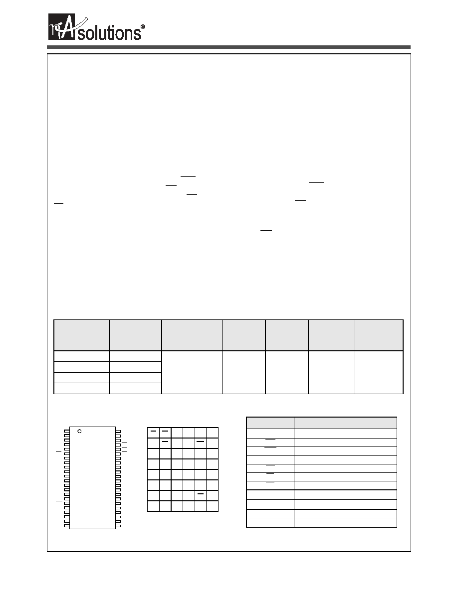
Pin Configuration (Top View)
Product Family
Part Number
Package Type
Operating
Temperature
Power
Supply (Vcc)
Speed
Standby
Current (I
SB
),
Max @ 3.0V
Operating
Current (Icc),
Max
N08T1630C2BZ
48 - BGA
-40
o
C to +85
o
C
2.7V - 3.6V
55/70ns @
2.7V
70
µA
3 mA @ 1MHz
N08T1630C2BZ2
Green 48 - BGA
N08T1630C1BT
44- TSOP2
N08T1630C1BT2 Green 44- TSOP2
1
2
3
4
5
6
7
8
9
10
11
12
13
14
15
16
17
18
19
20
21
22
A
4
A
3
A
2
A
1
A
0
CE
I/O
0
I/O
1
I/O
2
I/O
3
VCC
VSS
I/O
4
I/O
5
I/O
6
I/O
7
WE
A
18
A
17
A
16
A
15
A
14
44
43
42
41
40
39
38
37
36
35
34
33
32
31
30
29
28
27
26
25
24
23
A
5
A
6
A
7
OE
UB
LB
I/O
15
I/O
14
I/O
13
I/O
12
VSS
VCC
I/O
11
I/O
10
I/O
9
I/O
8
A
8
A
9
A
10
A
11
A
12
A
13
44 Pin
TSOP2
1
2
3
4
5
6
A
LB
OE
A
0
A
1
A
2
CE2
B
I/O
8
UB
A
3
A
4
CE1
I/O
0
C
I/O
9
I/O
10
A
5
A
6
I/O
1
I/O
2
D
V
SS
I/O
11
A
17
A
7
I/O
3
V
CC
E
V
CC
I/O
12
V
SS
A
16
I/O
4
V
SS
F
I/O
14
I/O
13
A
14
A
15
I/O
5
I/O
6
G
I/O
15
NC
A
12
A
13
WE
I/O
7
H
A
18
A
8
A
9
A
10
A
11
NC
48 Ball BGA
6 x 8 mm
Pin Descriptions
Pin Name
Pin Function
A
0
-A
18
Address Inputs
WE
Write Enable Input
CE1
Chip Enable 1 Input
CE2
Chip Enable 2 Input (BGA only)
OE
Output Enable Input
LB
Lower Byte Enable Input
UB
Upper Byte Enable Input
I/O
0
-I/O
15
Data Inputs/Outputs
V
CC
Power
V
SS
Ground
NC
Not Connected
(DOC# 14-02-004 REV H ECN# 01-1102)
2
The specifications of this device are subject to change without notice. For latest documentation see http://www.nanoamp.com.
NanoAmp Solutions, Inc.
N08T1630CxB
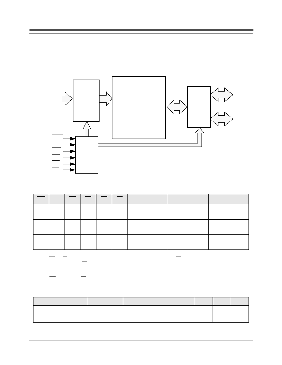
Functional Block Diagram
Functional Description
CE1
CE2
1
1. CE2 only applies to BGA package.
WE
OE
UB
LB
I/O
0
- I/O
15
2
2. When UB and LB are in select mode (low), I/O
0
- I/O
15
are affected as shown. When LB only is in the select mode only I/O
0
- I/O
7
are affected as shown. When UB is in the select mode only I/O
8
- I/O
15
are affected as shown.
MODE
POWER
H
X
X
X
X
X
High Z
Standby
3
3. When the device is in standby mode, control inputs (WE, OE, UB, and LB), address inputs and data input/outputs are internally
isolated from any external influence and disabled from exerting any influence externally.
Standby
X
L
X
X
X
X
High Z
Standby
3
Standby
L
H
X
X
H
H
High Z
Standby
3
Standby
L
H
L
X
4
4. When WE is invoked, the OE input is internally disabled and has no effect on the circuit.
L
2
L
2
Data In
Write
Active
L
H
H
L
L
2
L
2
Data Out
Read
Active
L
H
H
H
L
2
L
2
High Z
Active
Active
Capacitance
1
1. These parameters are verified in device characterization and are not 100% tested
Item
Symbol
Test Condition
Min
Max
Unit
Input Capacitance
C
IN
V
IN
= 0V, f = 1 MHz, T
A
= 25
o
C
8
pF
I/O Capacitance
C
I/O
V
IN
= 0V, f = 1 MHz, T
A
= 25
o
C
8
pF
Address
Inputs
A0 - A18
512K
x 16 bit
RAM Array
Input/
Output
Mux
and
Buffers
Address
Decode
Logic
Control
Logic
CE1
CE2
WE
OE
UB
LB
I/O0 - I/O7
I/O8 - I/O15
(DOC# 14-02-004 REV H ECN# 01-1102)
3
The specifications of this device are subject to change without notice. For latest documentation see http://www.nanoamp.com.
NanoAmp Solutions, Inc.
N08T1630CxB
Absolute Maximum Ratings
1
1. Stresses greater than those listed above may cause permanent damage to the device. This is a stress rating only and functional
operation of the device at these or any other conditions above those indicated in the operating section of this specification is not
implied. Exposure to absolute maximum rating conditions for extended periods may affect reliability.
Item
Symbol
Rating
Unit
Voltage on any pin relative to V
SS
V
IN,OUT
0.3 to V
CC
+0.3
V
Voltage on V
CC
Supply Relative to V
SS
V
CC
0.3 to 4.5
V
Power Dissipation
P
D
500
mW
Storage Temperature
T
STG
40 to 125
o
C
Operating Temperature
T
A
-40 to +85
o
C
Soldering Temperature and Time
T
SOLDER
260
o
C, 10sec
o
C
Operating Characteristics (Over Specified Temperature Range)
Item
Symbol
Test Conditions
Min.
Typ
1
1. Typical values are measured at Vcc=Vcc Typ., T
A
=25°C and not 100% tested.
Max
Unit
Supply Voltage
V
CC
2.7
3.0
3.6
V
Input High Voltage
V
IH
2.2
V
CC
+0.3
V
Input Low Voltage
V
IL
0.3
0.6
V
Output High Voltage
V
OH
I
OH
= 0.2mA
V
CC
0.4
V
Output Low Voltage
V
OL
I
OL
= -0.2mA
0.4
V
Input Leakage Current
I
LI
V
IN
= 0 to V
CC
0.5
µA
Output Leakage Current
I
LO
OE = V
IH
or Chip Disabled
0.5
µA
Read/Write Operating Supply Current
@ 1
µs Cycle Time
2
2. This parameter is specified with the outputs disabled to avoid external loading effects. The user must add current required to drive
output capacitance expected in the actual system.
I
CC1
V
CC
=3.6 V, V
IN
=V
IH
or V
IL
Chip Enabled, I
OUT
= 0
3.0
5.0
mA
Read/Write Operating Supply Current
@ 70 ns Cycle Time
2
I
CC2
V
CC
=3.6 V, V
IN
=V
IH
or V
IL
Chip Enabled, I
OUT
= 0
12.0
25.0
mA
Maximum Standby Current
I
SB1
V
IN
= V
CC
or 0V
Chip Disabled
t
A
= 85
o
C, V
CC
= 3.0 V
70.0
µA
Maximum Standby Current
I
SB2
V
IN
= V
CC
or 0V
Chip Disabled
t
A
= 85
o
C, V
CC
= 3.6 V
80.0
µA
(DOC# 14-02-004 REV H ECN# 01-1102)
4
The specifications of this device are subject to change without notice. For latest documentation see http://www.nanoamp.com.
NanoAmp Solutions, Inc.
N08T1630CxB
Timing
Item
Symbol
-55
-70
Units
Min.
Max.
Min.
Max.
Read Cycle Time
t
RC
55
70
ns
Address Access Time
t
AA
55
70
ns
Chip Enable to Valid Output
t
CO
55
70
ns
Output Enable to Valid Output
t
OE
30
35
ns
Byte Select to Valid Output
t
LB
, t
UB
55
70
ns
Chip Enable to Low-Z output
t
LZ
5
5
ns
Output Enable to Low-Z Output
t
OLZ
5
5
ns
Byte Select to Low-Z Output
t
BLZ
5
5
ns
Chip Disable to High-Z Output
t
HZ
0
20
0
25
ns
Output Disable to High-Z Output
t
OHZ
0
20
0
25
ns
Byte Select Disable to High-Z Output
t
BHZ
0
20
0
25
ns
Output Hold from Address Change
t
OH
10
10
ns
Write Cycle Time
t
WC
55
70
ns
Chip Enable to End of Write
t
CW
45
55
ns
Address Valid to End of Write
t
AW
45
55
ns
Byte Select to End of Write
t
BW
45
55
ns
Write Pulse Width
t
WP
45
55
ns
Address Setup Time
t
AS
0
0
ns
Write Recovery Time
t
WR
0
0
ns
Write to High-Z Output
t
WHZ
25
25
ns
Data to Write Time Overlap
t
DW
40
40
ns
Data Hold from Write Time
t
DH
0
0
ns
End Write to Low-Z Output
t
OW
5
5
ns
(DOC# 14-02-004 REV H ECN# 01-1102)
5
The specifications of this device are subject to change without notice. For latest documentation see http://www.nanoamp.com.
NanoAmp Solutions, Inc.
N08T1630CxB
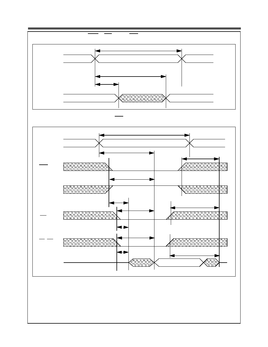
Timing of Read Cycle (CE1 = OE = V
IL
, WE = CE2 = V
IH
)
Timing Waveform of Read Cycle (WE=V
IH
)
Address
Data Out
t
RC
t
AA
t
OH
Data Valid
Previous Data Valid
Address
LB, UB
OE
Data Valid
t
RC
t
AA
t
CO
t
HZ
t
OHZ
t
BHZ
t
OLZ
t
OE
t
LZ
High-Z
Data Out
t
LB,
t
UB
t
LBLZ,
t
UBLZ
CE1
CE2