NanoAmp Solutions, Inc.
1982 Zanker Road, San Jose, CA 95112
ph: 408-573-8878, FAX: 408-573-8877
www.nanoamp.com
N32T163WA1(D1)A
Stock No. 23202-03 12/02
1
The specifications of this device are subject to change without notice. For latest documentation see http://www.nanoamp.com.
Advance Information
32Mb Ultra-Low Power Asynchronous CMOS Pseudo SRAM
2M x 16 bit
Overview
The N32T163WA1(D1)A is an integrated memory
device containing a 32Mbit SRAM built using a
self-refresh DRAM array organized as 2,097,152
words by 16 bits. The device is designed and
fabricated using NanoAmp's advanced CMOS
technology to provide both high-speed
performance and ultra-low power. It is designed to
be identical in operation and interface to standard
6T SRAMS. Byte controls (UB and LB) allow the
upper and lower bytes to be accessed
independently and can also be used to deselect
the device. The N32T163WA1(D1)A is optimal for
various applications where low-power is critical
such as battery backup and hand-held devices.
The device includes a power-down feature to
automatically enter standby mode as well as
several other power saving modes: a deep sleep
mode where data is not retained in the array and
partial array refresh mode where data is retained in
a portion of the array. Both these modes reduce
standby current drain. The VFBGA package offers
an extremely thin, low-profile size for today's space
conscience applications.
The device can operate over a very wide
temperature range of -25
o
C to +85
o
C and is
available in a JEDEC standard BGA package
compatible with other standard x 16 SRAMs.
Features
� Dual voltage for Optimum Performance:
Vccq - 1.7 Volts to Vcc
Vcc - 2.3 to 3.3 Volts
� Very low standby current
40�A V (Typical)
� Very low operating current
1.0mA at 1�s (Typical)
� Simple memory control
Byte control for independent byte operation
Output Enable (OE) for memory expansion
� Very fast output enable access time
35ns OE access time
� Automatic power down to standby mode
� TTL compatible three-state output driver
Pin Configuration
Product Family
Part Number
Package
Type
Operating
Temperature
Power
Supply
Speed
Standby
Current (I
SB
),
Max
Operating
Current (Icc),
Max
N32T163WA1AZ
48 - BGA
-25
o
C to +85
o
C
2.3V - 3.3V (V
CC
)
1.7V - Vcc(V
CCQ
)
70ns
85ns
100
�A
2 mA @ 1MHz
N32T163WD1AZ
1
2
3
4
5
6
A
LB
OE
A
0
A
1
A
2
ZZ
B
I/O
8
UB
A
3
A
4
CE
I/O
0
C
I/O
9
I/O
10
A
5
A
6
I/O
1
I/O
2
D
V
SSQ
I/O
11
A
17
A
7
I/O
3
V
CC
E
V
CCQ
I/O
12
DNU
A
16
I/O
4
V
SS
F
I/O
14
I/O
13
A
14
A
15
I/O
5
I/O
6
G
I/O
15
A
19
A
12
A
13
WE
I/O
7
H
A
18
A
8
A
9
A
10
A
11
A
20
48 Pin BGA (top)
8 x 10 mm
Pin Descriptions
Pin Name
Pin Function
A
0
-A
20
Address Inputs
WE
Write Enable Input
CE
Chip Enable Input
OE
Output Enable Input
UB,LB
Byte Enable Inputs
ZZ
Deep Sleep Input
I/O
0
-I/O
15
Data Inputs/Outputs
V
CC
Core Power
V
CCQ
I/O Power
V
SS
Ground
V
SSQ
I/O Ground
DNU
To be left floating or tied to V
SS
Stock No. 23202-03 12/02
2
The specifications of this device are subject to change without notice. For latest documentation see http://www.nanoamp.com.
NanoAmp Solutions, Inc.
N32T163WA1(D1)A
Advance Information
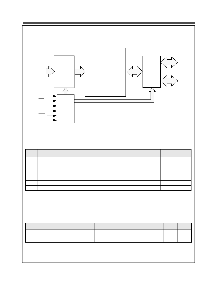
Functional Block Diagram
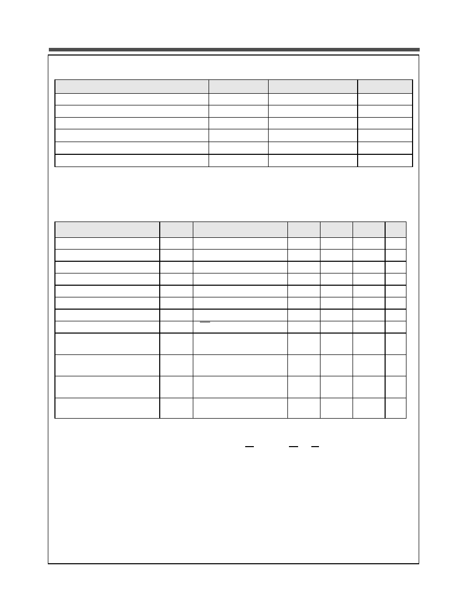
Functional Description
CE
ZZ
WE
OE
UB
LB
I/O
0
- I/O
15
1
1. When UB and LB are in select mode (low), I/O
0
- I/O
15
are affected as shown. When LB only is in the select mode only I/O
0
- I/O
7
are affected as shown. When UB is in the select mode only I/O
8
- I/O
15
are affected as shown.
MODE
POWER
H
H
X
X
X
X
High Z
Standby
2
2. When the device is in standby mode, control inputs (WE, OE, UB, and LB), address inputs and data input/outputs are internally
isolated from any external influence and disabled from exerting any influence externally.
Standby
X
H
X
X
H
H
High Z
Standby
2
Standby
L
H
L
X
3
3. When WE is invoked, the OE input is internally disabled and has no effect on the circuit.
L
1
L
1
Data In
Write
Active
L
H
H
L
L
1
L
1
Data Out
Read
Active
L
H
H
H
L
L
High Z
Active
Active
X
L
X
X
X
X
High Z
Deep Sleep
Deep Sleep
Capacitance
1
1. These parameters are verified in device characterization and are not 100% tested
Item
Symbol
Test Condition
Min
Max
Unit
Input Capacitance
C
IN
V
IN
= 0V, f = 1 MHz, T
A
= 25
o
C
6
pF
I/O Capacitance
C
I/O
V
IN
= 0V, f = 1 MHz, T
A
= 25
o
C
8
pF
Address
Inputs
A0 - A20
2Mb
x 16 bit
RAM Array
Input/
Output
Mux
and
Buffers
Page
Address
Decode
Logic
Control
Logic
CE
ZZ
WE
OE
UB
LB
I/O0 - I/O7
I/O8 - I/O15
Stock No. 23202-03 12/02
3
The specifications of this device are subject to change without notice. For latest documentation see http://www.nanoamp.com.
NanoAmp Solutions, Inc.
N32T163WA1(D1)A
Advance Information
Absolute Maximum Ratings
1
1. Stresses greater than those listed above may cause permanent damage to the device. This is a stress rating only and functional
operation of the device at these or any other conditions above those indicated in the operating section of this specification is not
implied. Exposure to absolute maximum rating conditions for extended periods may affect reliability.
Item
Symbol
Rating
Unit
Voltage on any pin relative to V
SS
V
IN,OUT
�0.2 to V
CC
+0.3
V
Voltage on V
CC
Supply Relative to V
SS
V
CC
�0.2 to 4.0
V
Power Dissipation
P
D
500
mW
Storage Temperature
T
STG
�40 to 125
o
C
Operating Temperature
T
A
-25 to +85
o
C
Soldering Temperature and Time
T
SOLDER
240
o
C, 10sec(Lead only)
o
C
Operating Characteristics (Over Specified Temperature Range)
Item
Symbol
Test Conditions
Min.
Typ
1
1. Typical values are measured at Vcc=Vcc Typ., T
A
=25�C and not 100% tested.
Max
Unit
Supply Voltage
V
CC
2.3
2.5
3.3
V
Supply Voltage for I/O
V
CCQ
1.7
2.5
Vcc
V
Input High Voltage
V
IH
1.4
V
CCQ
+0.2
V
Input Low Voltage
V
IL
�0.2
0.4
V
Output High Voltage
V
OH
I
OH
= -0.1mA
V
CCQ
�0.2
V
Output Low Voltage
V
OL
I
OL
= 0.1mA
0.2
V
Input Leakage Current
I
LI
V
IN
= 0 to V
CC
-1
+1
�A
Output Leakage Current
I
LO
OE = V
IH
or Chip Disabled
-1
+1
�A
Read/Write Operating Supply
Current @ 1
�s Cycle Time
2
2. This parameter is specified with the outputs disabled to avoid external loading effects. The user must add current required to
drive output capacitance expected in the actual system.
I
CC1
V
CC
= Max, V
IN
=CMOS levels-
Chip Enabled, I
OUT
= 0
2.0
mA
Read/Write Operating Supply
Current @ 70 ns Cycle Time
2
I
CC2
V
CC
= Max, V
IN
=CMOS levels
Chip Enabled, I
OUT
= 0
21.0
mA
Read/Write Operating Supply
Current @ 85 ns Cycle Time
2
I
CC3
V
CC
= Max, V
IN
=CMOS levels
Chip Enabled, I
OUT
= 0
18.0
mA
Maximum Standby Current
3
3. This device assumes a standby mode if the chip is disabled (either CE high or both UB and LB high). In order to achieve low
standby current all inputs must be within 0.2V of either VCC or VSS.
I
SB1
V
CC
= Max, V
IN
=CMOS levels
Chip Disabled
100.0
�A
Stock No. 23202-03 12/02
4
The specifications of this device are subject to change without notice. For latest documentation see http://www.nanoamp.com.
NanoAmp Solutions, Inc.
N32T163WA1(D1)A
Advance Information
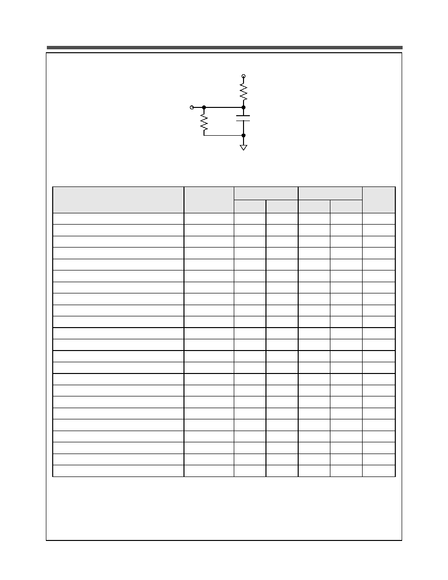
FIGURE 1: Output Load Circuit
Timing
Item
Symbol
85ns
70ns
Units
Min.
Max.
Min.
Max.
Read Cycle Time
t
RC
85
70
ns
Address Access Time (Random Access)
t
AA
85
70
ns
Chip Enable to Valid Output
t
CO
85
70
ns
Output Enable to Valid Output
t
OE
35
35
ns
Byte Select to Valid Output
t
LB
, t
UB
85
70
ns
Chip Enable to Low-Z output
t
LZ
10
10
ns
Output Enable to Low-Z Output
t
OLZ
5
5
ns
Byte Select to Low-Z Output
t
LBZ
, t
UBZ
10
10
ns
Chip Disable to High-Z Output
t
HZ
25
25
ns
Output Disable to High-Z Output
t
OHZ
25
25
ns
Byte Select Disable to High-Z Output
t
LBHZ
, t
UBHZ
25
25
ns
Output Hold from Address Change
t
OH
10
10
ns
Write Cycle Time
t
WC
85
70
ns
Chip Enable to End of Write
t
CW
75
60
ns
Address Valid to End of Write
t
AW
75
60
ns
Byte Select to End of Write
t
LBW
, t
UBW
75
60
ns
Write Pulse Width
t
WP
65
1000
50
1000
ns
Address Setup Time
t
AS
0
0
ns
Write Recovery Time
t
WR
0
0
ns
Write to High-Z Output
t
WHZ
25
25
ns
Data to Write Time Overlap
t
DW
30
30
ns
Data Hold from Write Time
t
DH
0
0
ns
End Write to Low-Z Output
t
OW
10
10
ns
V
CCQ
30 pF
I/O
14.5K
14.5K
Stock No. 23202-03 12/02
5
The specifications of this device are subject to change without notice. For latest documentation see http://www.nanoamp.com.
NanoAmp Solutions, Inc.
N32T163WA1(D1)A
Advance Information
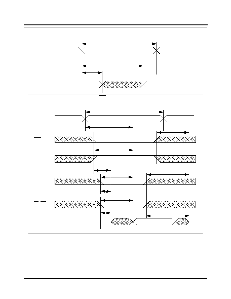
Timing of Read Cycle (CE1 = OE = V
IL
, WE = CE2 = V
IH
)
Timing Waveform of Read Cycle (WE=V
IH
)
Address
Data Out
t
RC
t
AA,
t
AAP
t
OH
Data Valid
Previous Data Valid
Address
LB, UB
OE
Data Valid
t
RC
t
AA,
t
AAP
t
CO
t
HZ
t
OHZ
t
LBHZ,
t
UBHZ
t
OLZ
t
OE
t
LZ
High-Z
Data Out
t
LB,
t
UB
t
LBLZ,
t
UBLZ
CE1
CE2