NT256D64SH8BAGM
256MB : 32M x 64
PC2700 / PC2100 Unbuffered DDR SO-DIMM
200pin Unbuffered DDR SO-DIMM
Based on DDR333/266 16Mx16 SDRAM
Features
∑
JEDEC Standard 200-Pin Small Outline Dual In-Line Memory
Module (SO-DIMM)
∑ 32Mx64 Double Unbuffered DDR SO-DIMM based on 16Mx16
DDR SDRAM.
∑ Performance:
PC2700
PC2100
Speed Sort
-6K
-75B
DIMM
CAS
Latency
2.5
2.5
Unit
f
CK
Clock Frequency
166
133 MHz
t
CK
Clock Cycle
6
7.5
ns
f
DQ
DQ Burst Frequency
333
266
MHz
∑ Intended for 133 MHz and 166 MHz applications
∑ Inputs and outputs are SSTL-2 compatible
∑ V
DD
= 2.5Volt ±
0.2, V
DDQ
= 2.5Volt ± 0.2
∑ SDRAMs have 4 internal banks for concurrent operation
∑ Module has two physical banks
∑ Differential clock inputs
∑ Data is read or written on both clock edges
∑ DRAM DLL aligns DQ and DQS transitions with clock
transitions.
∑ Address and control signals are fully synchronous to positive
clock edge
∑ Programmable Operation:
- DIMM
CAS
Latency: 2, 2.5
- Burst Type: Sequential or Interleave
- Burst Length: 2, 4, 8
- Operation: Burst Read and Write
∑ Auto Refresh (CBR) and Self Refresh Modes
∑ Automatic and controlled precharge commands
∑ 13/9/2 Addressing (row/column/bank)
∑ 7.8
µ
s Max. Average Periodic Refresh Interval
∑ Serial Presence Detect
∑ Gold contacts
∑ SDRAMs in 66-pin TSOP Type II Package
D
escription
NT256D64SH8BAGM is an unbuffered 200-Pin Double Data Rate (DDR) Synchronous DRAM Small Outline Dual In-Line Memory
Module (SO-DIMM), organized as a two-bank 32Mx64 high-speed memory array. The module uses eight 16Mx16 DDR SDRAMs in 400
mil TSOP II packages. These DIMMs are manufactured using raw cards developed for broad industry use as reference designs. The
use of these common design files minimizes electrical variation between suppliers. All NANYA DDR SDRAM DIMMs provide a
high-performance, flexible 8-byte interface in a 2.66" long space-saving footprint.
The DIMM is intended for use in applications operating up to 166 MHz clock speeds and achieves high-speed data transfer rates of up to
333 MHz. Prior to any access operation, the device
CAS
latency and burst type/ length/operation type must be programmed into the
DIMM by address inputs A0-A12 and I/O inputs BA0 and BA1 using the mode register set cycle.
The DIMM uses serial presence-detect implemented via a serial 2,048-bit EEPROM using a standard IIC protocol. The first 128 bytes of
serial PD data are programmed and locked during module assembly. The remaining 128 bytes are available for use by the customer.
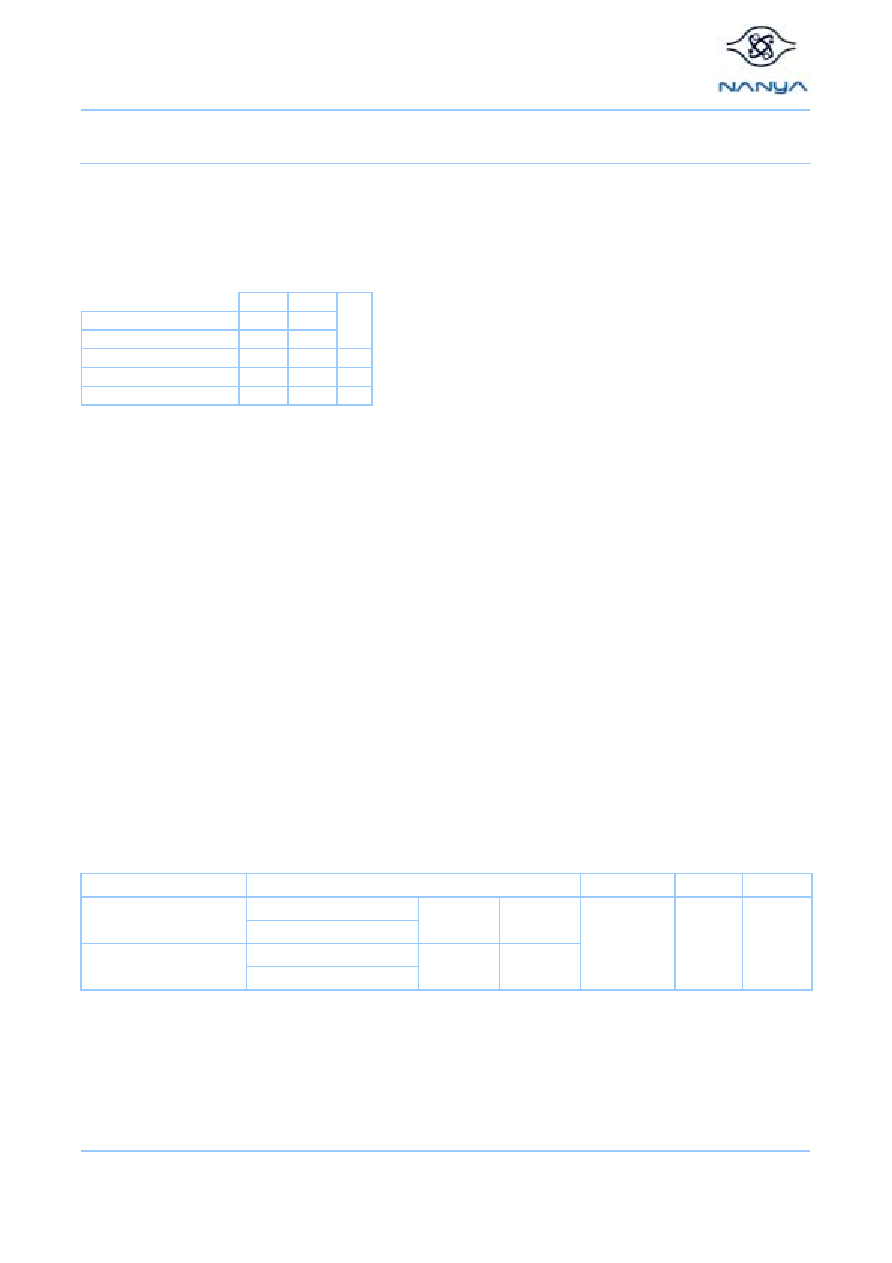
O
rdering Information
Part Number
Speed Organization
Leads
Power
166MHz (6ns @ CL = 2.5)
NT256D64SH8BAGM-6K
133MHz (7.5ns @ CL = 2)
DDR333 PC2700
133MHz (7.5ns @ CL = 2.5)
NT256D64SH8BAGM-75B
100MHz (10ns @ CL = 2)
DDR266B
PC2100
32Mx64 Gold 2.5V
REV 1.0
1
02/2003
© NANYA TECHNOLOGY CORP.
NANYA TECHNOLOGY CORP. reserves the right to change Products and Specifications without notice.

NT256D64SH8BAGM
256MB : 32M x 64
PC2700 / PC2100 Unbuffered DDR SO-DIMM
P
in Description
CK0, CK1, CK2,
CK0
,
CK1
,
CK2
Differential Clock Inputs
DQ0-DQ63
Data input/output
CKE0, CKE1
Clock Enable
DQS0-DQS7
Bi-directional data strobes
RAS
Row
Address
Strobe
DM0-DM7 Data
Masks
CAS
Column
Address
Strobe V
DD
Power
(2.5V)
WE
Write
Enable V
DDQ
Supply voltage for DQs(2.5V)
S0
,
S1
Chip
Selects V
SS
Ground
A0-A9, A11, A12
Address Inputs
NC
No Connect
A10/AP Address
Input/Autoprecharge
SCL Serial Presence Detect Clock Input
BA0, BA1
SDRAM Bank Address Inputs
SDA
Serial Presence Detect Data input/output
V
REF
Ref. Voltage for SSTL_2 inputs
SA0-2
Serial Presence Detect Address Inputs
V
DDID
V
DD
Identification flag.
V
DDSPD
Serial EEPROM positive power supply (2.5V)
P
inout
Pin Front Pin Back Pin Front Pin
Back Pin
Front
Pin
Back
Pin Front Pin
Back
1 V
REF
2 V
REF
51 V
SS
52
V
SS
101
A9 102
A8 151 DQ42 152
DQ46
3 V
SS
4 V
SS
53 DQ19 54
DQ23
103
V
SS
104
V
SS
153 DQ43 154
DQ47
5 DQ0 6 DQ4 55 DQ24 56
DQ28
105
A7 106
A6
155 V
DD
156
V
DD
7 DQ1 8 DQ5 57 V
DD
58
V
DD
107
A5 108
A4 157 V
DD
158
CK1
9 V
DD
10 V
DD
59 DQ25 60
DQ29
109
A3 110
A2 159 V
SS
160
CK1
11 DQS0 12 DM0 61 DQS3 62
DM3 111
A1 112
A0 161 V
SS
162
V
SS
13 DQ2 14 DQ6 63 V
SS
64
V
SS
113
V
DD
114
V
DD
163 DQ48 164
DQ52
15 V
SS
16 V
SS
65 DQ26 66
DQ30
115
A10/AP
116
BA1
165
DQ49
166
DQ53
17 DQ3 18 DQ7 67 DQ27 68
DQ31
117
V
DD
118
RAS
167 V
DD
168
V
DD
19 DQ8 20 DQ12 69 V
DD
70
V
DD
119
WE
120
CAS
169 DQS6 170
DM6
21 V
DD
22 V
DD
71 NC 72
NC 121
S0
122
S1
171 DQ50 172
DQ54
23 DQ9
24 DQ13 73 NC 74
NC 123
DU 124
DU
173 V
SS
174
V
SS
25 DQS1 26 DM1 75 V
SS
76
V
SS
125
V
SS
126
V
SS
175 DQ51 176
DQ55
27 V
SS
28 V
SS
77
DQS8 78
NC 127
DQ32
128
DQ36
177
DQ56
178
DQ60
29 DQ10 30 DQ14 79 NC 80
NC 129
DQ33
130
DQ37
179 V
DD
180
V
DD
31 DQ11 32 DQ15 81 V
DD
82
V
DD
131
V
DD
132
V
DD
181 DQ57 182
DQ61
33 V
DD
34 V
DD
83 NC 84
NC 133
DQS4
134
DM4
183
DQS7
184
DM7
35 CK0 36 V
DD
85 DU 86
DU 135
DQ34
136
DQ38
185 V
SS
186
V
SS
37
CK0
38 V
SS
87 V
SS
88
V
SS
137
V
SS
138
V
SS
187 DQ58 188
DQ62
39 V
SS
40 V
SS
89 CK2 90
V
SS
139
DQ35
140
DQ39
189 DQ59 190
DQ63
41 DQ16 42 DQ20 91
CK2
92
V
DD
141
DQ40
142
DQ44
191 V
DD
192
V
DD
43 DQ17 44 DQ21 93 V
DD
94
V
DD
143
V
DD
144
V
DD
193 SDA 194
SA0
45 V
DD
46 V
DD
95 CKE1 96
CKE0
145
DQ41
146
DQ45
195 SCL 196
SA1
47 DQS2 48 DM2 97 DU 98
DU 147
DQS5
148
DM5
197
V
DDSPD
198
SA2
49 DQ18 50 DQ22 99 A12 100
A11 149
V
SS
150
V
SS
199 V
DDID
200
DU
Note: All pin assignments are consistent for all 8-byte unbuffered versions.
REV 1.0
2
02/2003
© NANYA TECHNOLOGY CORP.
NANYA TECHNOLOGY CORP. reserves the right to change Products and Specifications without notice.

NT256D64SH8BAGM
256MB : 32M x 64
PC2700 / PC2100 Unbuffered DDR SO-DIMM
I
nput/Output Functional Description
Symbol
Type
Polarity
Function
CK0, CK1, CK2,
CK0
,
CK1
,
CK2
(SSTL)
Cross
point
The system clock inputs. All address and command lines are sampled on the cross point
of the rising edge of CK and falling edge of CK. A Delay Locked Loop (DLL) circuit is
driven from the clock inputs and output timing for read operations is synchronized to the
input clock.
CKE0, CKE1
(SSTL)
Active
High
Activates the DDR SDRAM CK signal when high and deactivates the CK signal when low.
By deactivating the clocks, CKE low initiates the Power Down mode or the Self Refresh
mode.
S0
,
S1
(SSTL)
Active
Low
Enables the associated DDR SDRAM command decoder when low and disables the
command decoder when high. When the command decoder is disabled, new commands
are ignored but previous operations continue. Physical Bank 0 is selected by S0; Bank 1 is
selected by S1.
RAS
,
CAS
,
WE
(SSTL)
Active
Low
When sampled at the positive rising edge of the clock,
RAS
,
CAS
,
WE
define the operation
to be executed by the SDRAM.
V
REF
Supply
Reference voltage for SSTL-2 inputs
V
DDQ
Supply
Isolated power supply for the DDR SDRAM output buffers to provide improved noise
immunity
BA0, BA1
(SSTL) - Selects which SDRAM bank is to be active.
A0 - A9
A10/AP
A11, A12
(SSTL) -
During a Bank Activate command cycle, A0-A12 defines the row address (RA0-RA12)
when sampled at the rising clock edge.
During a Read or Write command cycle, A0-A9 defines the column address (CA0-CA9)
when sampled at the rising clock edge. In addition to the column address, AP is used to
invoke autoprecharge operation at the end of the Burst Read or Write cycle. If AP is high,
autoprecharge is selected and BA0/BA1 define the bank to be precharged. If AP is low,
autoprecharge is disabled.
During a Precharge command cycle, AP is used in conjunction with BA0/BA1 to control
which bank(s) to precharge. If AP is high all 4 banks will be precharged regardless of the
state of BA0/BA1. If AP is low, then BA0/BA1 are used to define which bank to pre-charge.
DQ0 - DQ63
(SSTL) -
Data and Check Bit input/output pins operate in the same manner as on conventional
DRAMs.
DQS0 - DQS7
(SSTL)
Active
High
Data strobes: Output with read data, input with write data. Edge aligned with read data,
centered on write data. Used to capture write data.
DM0 ≠ DM7
Input
Active
High
The data write masks, associated with one data byte. In Write mode, DM operates as a
byte mask by allowing input data to be written if it is low but blocks the write operation if it
is high. In Read mode, DM lines have no effect. DM8 is associated with check bits
CB0-CB7, and is not used on x64 modules.
V
DD,
V
SS
Supply
Power and ground for the DDR SDRAM input buffers and core logic
SA0 ≠ SA2
-
Address inputs. Connected to either V
DD
or V
SS
on the system board to configure the
Serial Presence Detect EEPROM address.
SDA
-
This bi-directional pin is used to transfer data into or out of the SPD EEPROM. A resistor
must be connected from the SDA bus line to V
DD
to act as a pullup.
SCL
-
This signal is used to clock data into and out of the SPD EEPROM. A resistor may be
connected from the SCL bus time to V
DD
to act as a pullup.
V
DDSPD
Supply
Serial EEPROM positive power supply.
REV 1.0
3
02/2003
© NANYA TECHNOLOGY CORP.
NANYA TECHNOLOGY CORP. reserves the right to change Products and Specifications without notice.

NT256D64SH8BAGM
256MB : 32M x 64
PC2700 / PC2100 Unbuffered DDR SO-DIMM
Functional Block Diagram
(2 Bank, 16Mx16 DDR SDRAMs)
S0
DM0
DQ0
DQ1
DQ2
DQ7
DQ4
DQ6
DQ5
DQ3
DQ8
DQ9
DQ10
DQ15
DQ12
DQ14
DQ13
DQ11
DQ16
DQ17
DQ18
DQ23
DQ20
DQ22
DQ21
DQ19
DQ24
DQ25
DQ26
DQ31
DQ28
DQ30
DQ29
DQ27
DQS0
DM4
DQS4
DM1
DQS1
DM2
DQS2
DM3
DQS3
DQ32
DQ33
DQ34
DQ39
DQ36
DQ38
DQ37
DQ35
DQ40
DQ41
DQ42
DQ47
DQ44
DQ46
DQ45
DQ43
DQS5
DM5
DQ48
DQ49
DQ50
DQ55
DQ52
DQ54
DQ53
DQ51
DQ56
DQ57
DQ58
DQ63
DQ60
DQ62
DQ61
DQ59
DQS6
DM6
DQS7
DM7
S1
Serial PD
A0
A2
A1
SCL
WP
SDA
SA0
SA2
SA1
V
DDSPD
V
SS
SPD
D0-D7
D0-D7
D0-D7
V
DD
/V
DDQ
V
REF
V
DDID
I/O 0
I/O 1
I/O 6
I/O 5
I/O 4
I/O 3
I/O 2
I/O 7
LDM
CS
D0
I/O 8
I/O 9
I/O 14
I/O 13
I/O 12
I/O 11
I/O 10
I/O 15
UDM
UDQS
LDQS
I/O 0
I/O 1
I/O 6
I/O 5
I/O 4
I/O 3
I/O 2
I/O 7
LDM
CS
D4
I/O 8
I/O 9
I/O 14
I/O 13
I/O 12
I/O 11
I/O 10
I/O 15
UDM
UDQS
LDQS
I/O 0
I/O 1
I/O 6
I/O 5
I/O 4
I/O 3
I/O 2
I/O 7
LDM
CS
D1
I/O 8
I/O 9
I/O 14
I/O 13
I/O 12
I/O 11
I/O 10
I/O 15
UDM
UDQS
LDQS
I/O 0
I/O 1
I/O 6
I/O 5
I/O 4
I/O 3
I/O 2
I/O 7
LDM
CS
D5
I/O 8
I/O 9
I/O 14
I/O 13
I/O 12
I/O 11
I/O 10
I/O 15
UDM
UDQS
LDQS
I/O 0
I/O 1
I/O 6
I/O 5
I/O 4
I/O 3
I/O 2
I/O 7
LDM
CS
D3
I/O 8
I/O 9
I/O 14
I/O 13
I/O 12
I/O 11
I/O 10
I/O 15
UDM
UDQS
LDQS
I/O 0
I/O 1
I/O 6
I/O 5
I/O 4
I/O 3
I/O 2
I/O 7
LDM
CS
D7
I/O 8
I/O 9
I/O 14
I/O 13
I/O 12
I/O 11
I/O 10
I/O 15
UDM
UDQS
LDQS
I/O 0
I/O 1
I/O 6
I/O 5
I/O 4
I/O 3
I/O 2
I/O 7
LDM
CS
D2
I/O 8
I/O 9
I/O 14
I/O 13
I/O 12
I/O 11
I/O 10
I/O 15
UDM
UDQS
LDQS
I/O 0
I/O 1
I/O 6
I/O 5
I/O 4
I/O 3
I/O 2
I/O 7
LDM
CS
D6
I/O 8
I/O 9
I/O 14
I/O 13
I/O 12
I/O 11
I/O 10
I/O 15
UDM
UDQS
LDQS
Notes :
1. DQ wiring may differ from that described in this drawing.
2. DQ/DQS/DM/CKE/S relationships are maintained as shown.
3. DQ/DQS/DM/DQS resistors are 22+/- 5% Ohms.
4. V
DDID
strap connections (for memory device V
DD
, V
DDQ
):
STRAP OUT (OPEN): V
DD
= V
DDQ
STRAP IN (V
SS
): V
DD
is not equal to V
DDQ
.
4 loads
CK0
CK0
CK1
CK1
CK2
CK2
4 loads
0 loads
A0-A12
RAS
BA0-BA1
BA0-BA1 : SDRAMs D0-D7
A0-A12 : SDRAMs D0-D7
RAS
: SDRAMs D0-D7
CKE0
WE
CAS
CAS
: SDRAMs D0-D7
CKE : SDRAMs D0-D3
CKE : SDRAMs D4-D7
WE
: SDRAMs D0-D7
CKE1
REV 1.0
4
02/2003
© NANYA TECHNOLOGY CORP.
NANYA TECHNOLOGY CORP. reserves the right to change Products and Specifications without notice.

NT256D64SH8BAGM
256MB : 32M x 64
PC2700 / PC2100 Unbuffered DDR SO-DIMM
Serial Presence Detect --
Part 1 of 2
32Mx64 SDRAM DIMM based on 16Mx16, 4Banks, 8K Refresh, 2.5V DDR SDRAMs with SPD
SPD Entry Value
Serial PD Data Entry
(Hexadecimal)
Note
Byte
Description
DDR333
-6K
DDR266B
-75B
DDR333
-6K
DDR266B
-75B
0
Number of Serial PD Bytes Written during Production
128
80
1
Total Number of Bytes in Serial PD device
256
08
2
Fundamental Memory Type
SDRAM DDR
07
3
Number of Row Addresses on Assembly
13
0D
4
Number of Column Addresses on Assembly
9
09
5
Number of DIMM Bank
2
02
6
Data Width of Assembly
X64
40
7
Data Width of Assembly (cont')
X64
00
8
Voltage Interface Level of this Assembly
SSTL 2.5V
04
9
DDR SDRAM Device Cycle Time at CL=2.5
6ns
7.5ns
60
75
10
DDR SDRAM Device Access Time from Clock at CL=2.5
0.7ns
0.75ns
70
75
11 DIMM
Configuration
Type
Non-Parity
00
12 Refresh
Rate/Type
SR/1x(7.8us)
82
13
Primary DDR SDRAM Width
X16
10
14
Error Checking DDR SDRAM Device Width
N/A
00
15
DDR SDRAM Device Attr: Min CLK Delay, Random Col
Access
1 Clock
01
16
DDR SDRAM Device Attributes: Burst Length Supported
2,4,8
0E
17
DDR SDRAM Device Attributes: Number of Device Banks
4
04
18
DDR SDRAM Device Attributes: CAS Latencies Supported
2/2.5
2/2.5
0C
0C
19
DDR SDRAM Device Attributes: CS Latency
0
01
20
DDR SDRAM Device Attributes: WE Latency
1
02
21 DDR
SDRAM
Device
Attributes: Differential
Clock
20
22
DDR SDRAM Device Attributes: General
+/-0.2V Voltage Tolerance
00
23
Minimum Clock Cycle at CL=2
7.5ns
10ns
75
A0
24
Maximum Data Access Time from Clock at CL=2
0.70ns
0.75ns
70
75
25
Minimum Clock Cycle Time at CL=1
N/A
00
26
Maximum Data Access Time from Clock at CL=1
N/A
00
27
Minimum Row Precharge Time (t
RP
) 18ns
20ns
48
50
28
Minimum Row Active to Row Active delay (t
RRD
) 12ns
15ns
30
3C
29
Minimum RAS to CAS delay (t
RCD
) 18ns
20ns
48
50
30
Minimum RAS Pulse Width (t
RAS
) 42ns
45ns
2A
2D
31
Module Bank Density
128MB
20
32
Address and Command Setup Time Before Clock
0.75ns
0.9ns
75
90
33
Address and Command Hold Time After Clock
0.75ns
0.9ns
75
90
34
Data Input Setup Time Before Clock
0.45ns
0.5ns
45
50
35
Data Input Hold Time After Clock
0.45ns
0.5ns
45
50
36-61 Reserved
Undefined
00
62 SPD
Revision
Initial
Initial
00
00
63 Checksum
Data
F2
A7
REV 1.0
5
02/2003
© NANYA TECHNOLOGY CORP.
NANYA TECHNOLOGY CORP. reserves the right to change Products and Specifications without notice.