
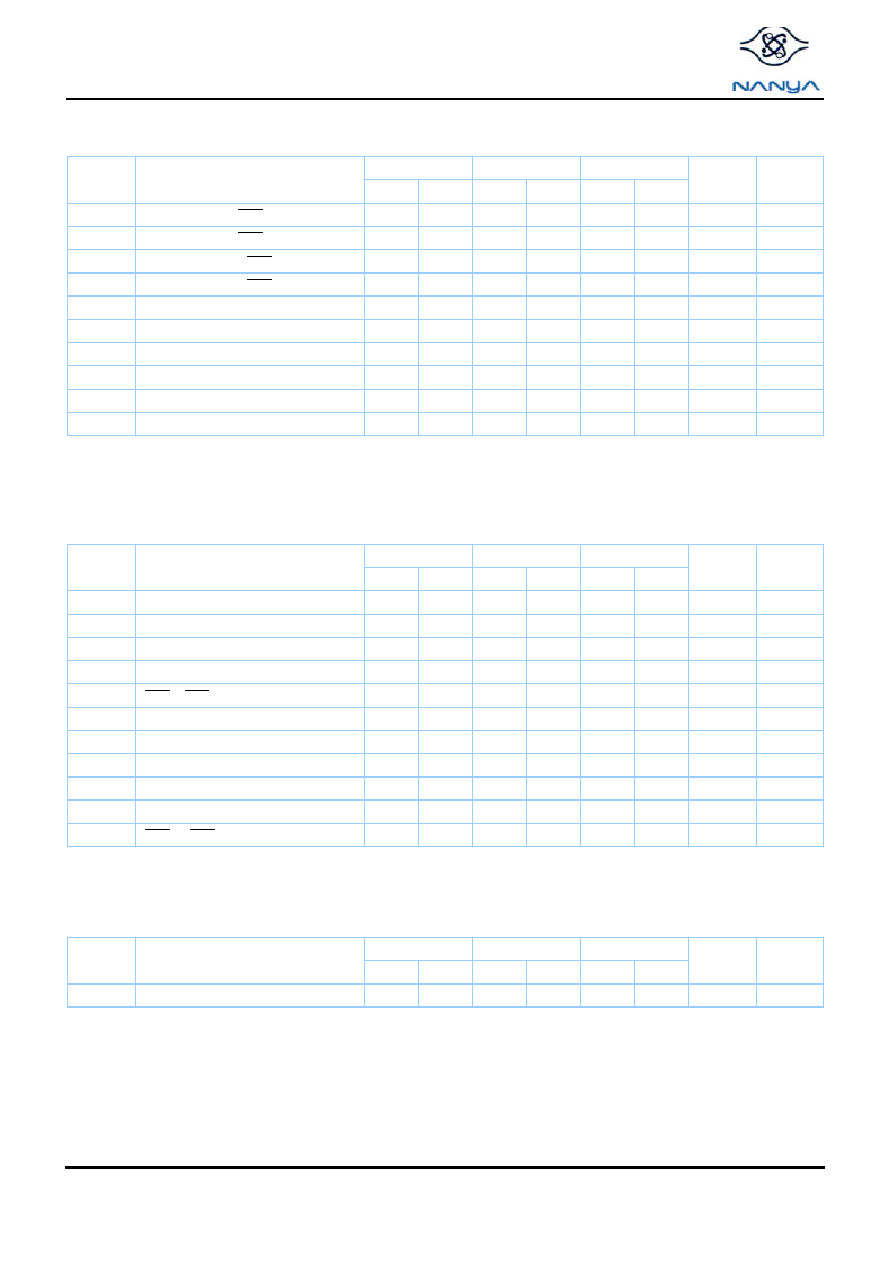
NT256S64VH8A0GM
256MB : 32M x 64
SDRAM SODIMM
PRELIMINARY
08 / 2001
1
© NANYA TECHNOLOGY CORP.
NANYA TECHNOLOGY CORP. reserves the right to change Products and Specifications without notice.
32Mx64 bit Two Bank Small Outline SDRAM Module
based on 16Mx16, 4Banks, 8K Refresh, 3.3V Synchronous DRAMs with SPD
Features
l
144 Pin JEDEC Standard, 8 Byte Small Outline Dual-In-line
Memory Module
l
32Mx64 Synchronous DRAM SO DIMM
l
Inputs and outputs are LVTTL (3.3V) compatible
l
10 Ohm Resistors on DQs
l
Single 3.3V
±
0.3V Power Supply
l
Single Pulsed RAS interface
l
SDRAMs have four internal banks
l
Fully Synchronous to positive Clock Edge
l
Data Mask for Byte Read/Write control
l
Auto Refresh (CBR) and Self Refresh
l
Automatic and controlled Precharge Commands
l
Programmable Operation:
- CAS Latency: 2, 3
- Burst Type: Sequential or Interleave
- Burst Length: 1, 2, 4, 8,
- Operation: Burst Read and Write or Multiple Burst Read with
Single Write
l
Suspend Mode and Power Down Mode
l
13/9/2 Addressing (Row/Column/Bank)
l
8192 refresh cycles distributed across 64ms
l
Serial Presence Detect
l
Gold contacts
Description
NT256S64VH8A0GM is a 144-pin Synchronous DRAM Small Outline Dual In-line Memory Module (SO DIMM) that is organized as a 32Mx64
high-speed memory array. The SO DIMM uses eight 16Mx16 SDRAMs in 400mil TSOP II packages and achieves high-speed data transfer
rates of up to 133 MHz by employing a prefetch / pipeline hybrid architecture that supports the JEDEC 1N rule while allowing very low burst
power.
All control, address, and data input/output circuits are synchronized with the positive edge of the externally supplied clock inputs. All inputs are
sampled at the positive edge of the externally supplied clock (CK0,CK1). Internal operating modes are defined by combinations of the
RAS , CAS , WE , S0 , S1, DQMB, and CKE0, CKE1signals. A command decoder initiates the necessary timings for each operation.
Prior to any access operation, the CAS latency, burst type, burst length, and burst operation type must be programmed into the SO DIMM by
address inputs A0-A9 during the mode register set cycle. The SO DIMM uses serial presence detects implemented via a serial EEPROM using
the two pin IIC protocol. The first 128 bytes of serial PD data are used by the DIMM manufacturer. The last 128 bytes are available to the
customer.
All Nanya 144-pin SO DIMMs provide a high performance, flexible 8-byte interface in a 2.66" long space-saving footprint.
Ordering Information
Speed
Part Number
MHz.
CL
t RCD
t RP
Organization
Leads
Power
143MHz
3
3
3
NT256S64VH8A0GM-7K
133MHz
2
2
2
133MHz
3
3
3
NT256S64VH8A0GM-75B
100MHz
2
2
2
125MHz
3
3
3
NT256S64VH8A0GM-8B
100MHz
2
2
2
32Mx64
Gold
3.3V
* CL =
CAS Latency
NT256S64VH8A0GM
256MB : 32M x 64
SDRAM SODIMM
PRELIMINARY
08 / 2001
2
© NANYA TECHNOLOGY CORP.
NANYA TECHNOLOGY CORP. reserves the right to change Products and Specifications without notice.
Pin Description
CK0,CK1
Clock Inputs
DQ0-DQ63
Data input/output
CKE0,CKE1
Clock Enable
DQMB0-DQMB7
Data Mask
RAS
Row Address Strobe
V
DD
Power (3.3V)
CAS
Column Address Strobe
V
SS
Ground
WE
Write Enable
NC
No Connect
S0 , S1
Chip Selects
SCL
Serial Presence Detect Clock Input
A0-A9, A11,A12
Address Inputs
SDA
Serial Presence Detect Data input/output
A10 / AP
Address Input/Autoprecharge
DU
Don't use
BA0, BA1
SDRAM Bank Address
Pinout
Pin
Front
Pin
Back
Pin
Front
Pin
Back
Pin
Front
Pin
Back
1
V
SS
2
V
SS
51
DQ14
52
DQ46
95
DQ21
96
DQ53
3
DQ0
4
DQ32
53
DQ15
54
DQ47
97
DQ22
98
DQ54
5
DQ1
6
DQ33
55
V
SS
56
V
SS
99
DQ23
100
DQ55
7
DQ2
8
DQ34
57
NC
58
NC
101
V
DD
102
V
DD
9
DQ3
10
DQ35
59
NC
60
NC
103
A6
104
A7
11
V
DD
12
V
DD
105
A8
106
BA0
13
DQ4
14
DQ36
107
V
SS
108
V
SS
15
DQ5
16
DQ37
Voltage Key
109
A9
110
BA1
17
DQ6
18
DQ38
61
CK0
62
CKE0
111
A10/ AP
112
A11
19
DQ7
20
DQ39
63
V
DD
64
V
DD
113
V
DD
114
V
DD
21
V
SS
22
V
SS
65
RAS
66
CAS
115
DQMB2
116
DQMB6
23
DQMB0
24
DQMB4
67
WE
68
CKE1
117
DQMB3
118
DQMB7
25
DQMB1
26
DQMB5
69
S0
70
A12
119
V
SS
120
V
SS
27
V
DD
28
V
DD
71
S1
72
NC
121
DQ24
122
DQ56
29
A0
30
A3
73
DU
74
CK1
123
DQ25
124
DQ57
31
A1
32
A4
75
V
SS
76
V
SS
125
DQ26
126
DQ58
33
A2
34
A5
77
NC
78
NC
127
DQ27
128
DQ59
35
V
SS
36
V
SS
79
NC
80
NC
129
V
DD
130
V
DD
37
DQ8
38
DQ40
81
V
DD
82
V
DD
131
DQ28
132
DQ60
39
DQ9
40
DQ41
83
DQ16
84
DQ48
133
DQ29
134
DQ61
41
DQ10
42
DQ42
85
DQ17
86
DQ49
135
DQ30
136
DQ62
43
DQ11
44
DQ43
87
DQ18
88
DQ50
137
DQ31
138
DQ63
45
V
DD
46
V
DD
89
DQ19
90
DQ51
139
V
SS
140
V
SS
47
DQ12
48
DQ44
91
V
SS
92
V
SS
141
SDA
142
SCL
49
DQ13
50
DQ45
93
DQ20
94
DQ52
143
V
DD
144
V
DD
Note: All pin assignments are consistent for all 8-byte versions.
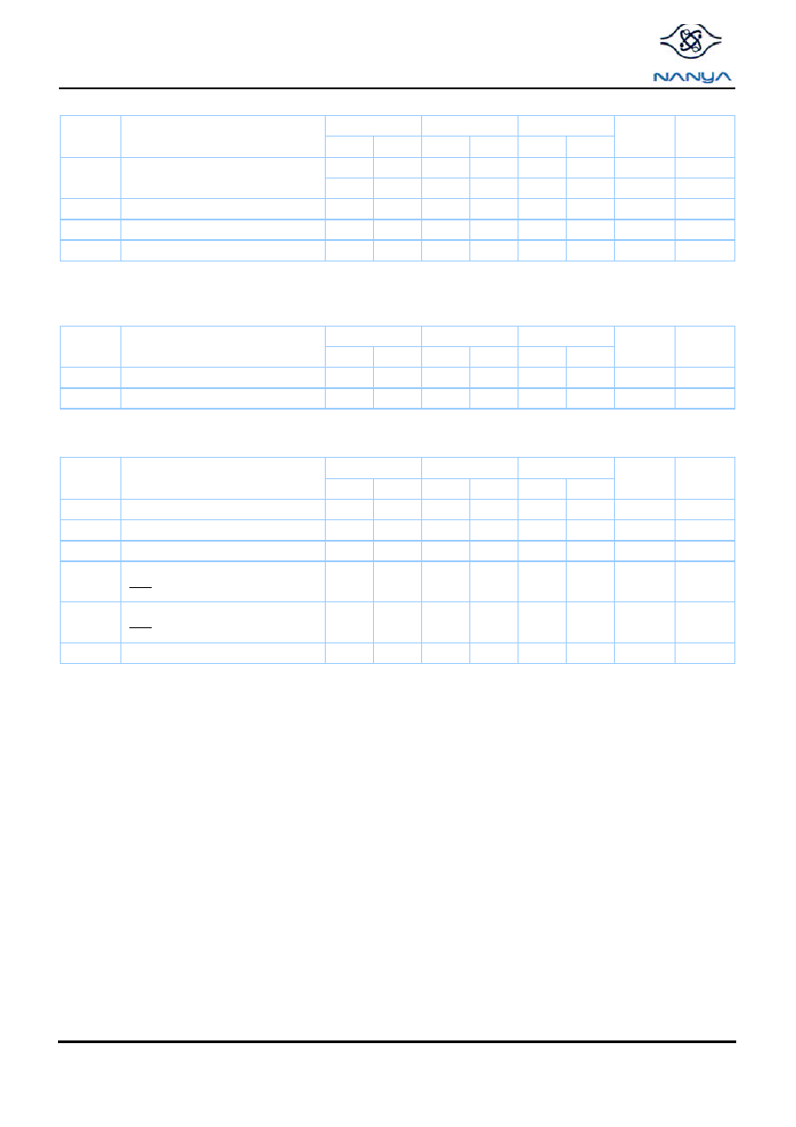
NT256S64VH8A0GM
256MB : 32M x 64
SDRAM SODIMM
PRELIMINARY
08 / 2001
3
© NANYA TECHNOLOGY CORP.
NANYA TECHNOLOGY CORP. reserves the right to change Products and Specifications without notice.
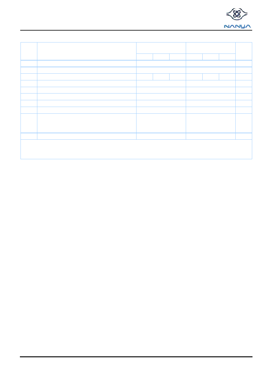
SDRAM DIMM Block Diagram
(2 Bank, 16Mx16 SDRAMs)
S0
DQMB0
LDQM
DQ0
DQ1
DQ2
DQ3
DQ4
DQ5
DQ6
DQ7
DQ0
DQ1
DQ2
DQ3
DQ4
DQ5
DQ6
DQ7
CS
D0
DQMB4
LDQM
DQ32
DQ33
DQ34
DQ35
DQ36
DQ37
DQ38
DQ39
DQ0
DQ1
DQ2
DQ3
DQ4
DQ5
DQ6
DQ7
CS
D2
DQMB1
UDQM
DQ8
DQ9
DQ10
DQ11
DQ12
DQ13
DQ14
DQ15
DQ8
DQ9
DQ10
DQ11
DQ12
DQ13
DQ14
DQ15
DQMB5
UDQM
DQ40
DQ41
DQ42
DQ43
DQ44
DQ45
DQ46
DQ47
DQ8
DQ9
DQ10
DQ11
DQ12
DQ13
DQ14
DQ15
RAS
CAS
CKE0
WE
A0-A12
BA0
BA1
SDRAMs D0-D7
SDRAMs D0-D7
SDRAMs D0-D3
SDRAMs D0-D7
SDRAMs D0-D7
SDRAMs D0-D7
SDRAMs D0-D7
SPD
A0
A1
A2
SCL
V
DD
V
SS
D0 - D7
D0 - D7
SDA
CK0 / CK1
CK1
10pF
DQMB2
LDQM
DQ16
DQ17
DQ18
DQ19
DQ20
DQ21
DQ22
DQ23
DQ0
DQ1
DQ2
DQ3
DQ4
DQ5
DQ6
DQ7
CS
D1
DQMB6
LDQM
DQ48
DQ49
DQ50
DQ51
DQ52
DQ53
DQ54
DQ55
DQ0
DQ1
DQ2
DQ3
DQ4
DQ5
DQ6
DQ7
CS
D3
DQMB3
UDQM
DQ24
DQ25
DQ26
DQ27
DQ28
DQ29
DQ30
DQ31
DQ8
DQ9
DQ10
DQ11
DQ12
DQ13
DQ14
DQ15
DQMB7
UDQM
DQ56
DQ57
DQ58
DQ59
DQ60
DQ61
DQ62
DQ63
DQ8
DQ9
DQ10
DQ11
DQ12
DQ13
DQ14
DQ15
10ohm
D0 / D4
D1 / D5
D2 / D6
D3 / D7
DQn
Every DQ pin of SDRAM
LDQM
DQ0
DQ1
DQ2
DQ3
DQ4
DQ5
DQ6
DQ7
CS
D4
UDQM
DQ8
DQ9
DQ10
DQ11
DQ12
DQ13
DQ14
DQ15
LDQM
DQ0
DQ1
DQ2
DQ3
DQ4
DQ5
DQ6
DQ7
CS
D6
UDQM
DQ8
DQ9
DQ10
DQ11
DQ12
DQ13
DQ14
DQ15
LDQM
DQ0
DQ1
DQ2
DQ3
DQ4
DQ5
DQ6
DQ7
CS
D5
UDQM
DQ8
DQ9
DQ10
DQ11
DQ12
DQ13
DQ14
DQ15
LDQM
DQ0
DQ1
DQ2
DQ3
DQ4
DQ5
DQ6
DQ7
CS
D7
UDQM
DQ8
DQ9
DQ10
DQ11
DQ12
DQ13
DQ14
DQ15
S1
CKE1
SDRAMs D4-D7

NT256S64VH8A0GM
256MB : 32M x 64
SDRAM SODIMM
PRELIMINARY
08 / 2001
4
© NANYA TECHNOLOGY CORP.
NANYA TECHNOLOGY CORP. reserves the right to change Products and Specifications without notice.
Input/Output Functional Description
Symbol
Type
Signal
Polarity
Function
CK0, CK1
Input
Pulse
Positive
Edge
The system clock inputs. All of the SDRAM inputs are sampled on the rising edge of
their associated clock.
CKE0, CKE1
Input
Level
Active
High
Activates the SDRAM CK0 and CK1 signals when high and deactivates them when low.
By deactivating the clocks, CKE0 low initiates the Power Down mode, Suspend mode, or
the Self-Refresh mode.
S0 , S1
Input
Pulse
Active
Low
Enables the associated SDRAM command decoder when low and disables the
command decoder when high. When the command decoder is disabled, new commands
are ignored but previous operations continue.
RAS
,
CAS
,
WE
Input
Pulse
Active
Low
When sampled at the positive rising edge of the clock, RAS
,
CAS
,
WE define the
operation to be executed by the SDRAM.
BA0, BA1
Input
Level
-
Selects which SDRAM bank is to be active.
A0 - A9
A10/AP
A11, A12
Input
Level
-
During a Bank Activate command cycle, A0-A12 defines the row address (RA0-RA12)
when sampled at the rising clock edge.
During a Read or Write command cycle, A0-A8 defines the column address (CA0-CA8)
when sampled at the rising clock edge. In addition to the column address, AP is used to
invoke Autoprecharge operation at the end of the Burst Read or Write cycle. If AP is high,
autoprecharge is selected and BA0/BA1 define the bank to be precharged. If AP is low,
autoprecharge is disabled.
During a Precharge command cycle, AP is used in conjunction with BA0/BA1 to control
which bank(s) to precharge. If AP is high all 4 banks will be precharged regardless of the
state of BA0/BA1. If AP is low, then BA0/BA1 are used to define which bank to
pre-charge.
DQ0 - DQ63
Input
/Output
Level
-
Data and Check Bit input/output pins operate in the same manner as on conventional
DRAMs.
DQMB0 -DQMB7
Input
Pulse
Active
High
The Data input/output mask places the DQ buffers in a high impedance state when
sampled high. In Read mode, DQM has a latency of two clock cycles and controls the
output buffers like an output enable. In Write mode, DQM has a latency of zero and
operates as a byte mask by allowing input data to be written if it is low but blocks the
Write operation if DQM is high.
SDA
Input
/Output
Level
-
Serial Data. Bi-directional signal used to transfer data into and out of the Serial Presence
Detect EEPROM. Since the SDA signal is Open Drain/Open Collector at the EEPROM, a
pull-up resistor is required on the system board.
SCL
Input
Pulse
-
Serial Clock. Used to clock all Serial Presence Detect data into and out of the EEPROM.
Since the SCL signal is inactive in the "high" state, a pull-up resistor is recommended on
the system board.
V
DD
, V
SS
Supply
Power and ground for the module.
NT256S64VH8A0GM
256MB : 32M x 64
SDRAM SODIMM
PRELIMINARY
08 / 2001
5
© NANYA TECHNOLOGY CORP.
NANYA TECHNOLOGY CORP. reserves the right to change Products and Specifications without notice.
Absolute Maximum Ratings
Symbol
Parameter
Rating
Units
Notes
V
DD,
V
DDQ
Voltage on V
DD
relative to V
SS
-0.3 to +4.6
V
IN,
V
OUT
Voltage on Any Pin to V
SS
-0.3 to V
DD
+ 0.3
V
1
T
A
Operating Temperature (ambient)
0 to +70
∞C
1
T
STG
Storage Temperature
-55 to +125
∞C
1
P
D
Power Dissipation
8
W
1
I
OUT
Short Circuit Output Current
50
mA
1
1.1. Stresses greater than those listed under "Absolute Maximum Ratings" may cause permanent damage to the device.
This is a stress rating only and functional operation of the device at these or any other conditions above those indicated in the operational
sections of this specification is not implied. Exposure to absolute maximum rating conditions for extended periods may affect reliability.
Recommended DC Operating Conditions
(T
A
=0 to 70
∞C)
Rating
Symbol
Parameter
Min.
Typ.
Max.
Units
Notes
V
DD
Power Voltage
3.0
3.3
3.6
V
1
V
IH
Input High Voltage
2.0
-
V
DD
+ 0.3
V
1,2
V
IL
Input Low Voltage
-0.3
-
0.8
V
1,3
V
OH
Output High Voltage
2.4
-
-
V
V
OL
Output Low Voltage
-
-
0.4
V
I
IL
Input Leakage current
-10
-
10
µA
1. All voltages referenced to V
SS
.
2. V
IH
(max) = V
DD
/ V
DDQ
+ 1.2V for pulse width
5ns
3.
V
IL
(min) = V
SS
/ V
SSQ
- 1.2V for pulse width
5ns .
Capacitance
(T
A
=25 ∞C , f =1MHz, V
DD
=3.3 ± 0.3V)
Symbol
Parameter
Max.
Unit
C
I1
Input Capacitance (A0-A9, A10/AP, A11, A12, BA0, BA1, RAS
,
CAS
,
WE )
52
C
I2
Input Capacitance (CKE0,CKE1)
46
C
I3
Input Capacitance ( S0 , S1)
35
C
I4
Input Capacitance (CK0,CK1 )
30
C
I5
Input Capacitance (DQMB0 - DQMB7)
15
C
I6
Input Capacitance (SCL)
13
C
IO1
Input/Output Capacitance (DQ0 - DQ63)
18
C
IO2
Input/Output Capacitance (SDA)
15
pF
DC Output Load Circuit
VOH(DC) = 2.4V,IOH= -2mA
VOL(DC) = 0.4V,IOL= -2mA
3.3 V
1200 ohms
870 ohms
50 pF
Output
NT256S64VH8A0GM
256MB : 32M x 64
SDRAM SODIMM
PRELIMINARY
08 / 2001
6
© NANYA TECHNOLOGY CORP.
NANYA TECHNOLOGY CORP. reserves the right to change Products and Specifications without notice.
Operating, Standby, and Refresh Currents
(T
A
=0 to 70 ∞C, V
DD
=3.3 ± 0.3V)
Speed
Parameter
Symbol
Test condition
- 7K
- 75B
- 8B
Unit
Note
Operating current
I
CC1
1 bank operation , t
RC
= t
RC
(mim), t
CK
= min
Active-Precharge Command cycling
without burst operation
1040
960
920
mA
1, 2
I
CC2P
CKE
V
IL
(max), t
CK
= min,
S0 , S1= V
IH
(min)
16
mA
Precharge
standby current
in power-down mode
I
CC2PS
CKE
V
IL
(max), t
CK
=oo ,
S0 , S1= V
IH
(min)
16
mA
I
CC2N
CKE
V
IH
(min), t
CK
= min
S0 , S1= V
IH
(min)
240
240
160
mA
3
Precharge
standby current in non
power-down mode
I
CC2NS
CKE
V
IH
(min), t
CK
=oo,
S0 , S1= V
IH
(min)
64
64
64
mA
4
I
CC3P
CKE
V
IL
(max), t
CK
=min.
S0 , S1= V
IH
(min) , (Power Down Mode)
48
48
48
mA
5
No Operating current
( Active state : 4 bank)
I
CC3N
CKE
V
IH
(min), t
CK
=min
S0 , S1= V
IH
(min)
480
480
360
mA
3
Operating current
( Burst mode )
I
CC4
t
CK
=min , Read/ Write command cycling,
Multiple banks active, gapless data, BL=4
960
960
720
mA
2, 6
Auto(CBR)
refresh current
I
CC5
t
CK
=min, CBR command cycling
1400
1400
1320
mA
Self refresh current
I
CC6
CKE
0.2V
24
mA
1. These parameters depend on the cycle rate and are measured with the cycle determined by the minimum value of t
CK
and t
RC
. Input
signals are changed up to three times during t
RC
(min).
2. The specified values are obtained with the output open.
3. Input signals are changed once during three clock cycles.
4. Input signals are stable.
5. Active standby current will be higher if Clock Suspend is entered during a Burst Read cycle (add 1mA per DQ).
6. Input signals are changed once during tCK(min) .
7. V
DD
=3.3V

NT256S64VH8A0GM
256MB : 32M x 64
SDRAM SODIMM
PRELIMINARY
08 / 2001
7
© NANYA TECHNOLOGY CORP.
NANYA TECHNOLOGY CORP. reserves the right to change Products and Specifications without notice.
AC Characteristics
(T
A
=0 to 70 ∞C , V
DD
=3.3 ± 0.3V)
1. An initial pause of 200µs,with DQMB0-7 and CKE held high, is required after power-up. A Precharge All Banks command must be given
followed by a minimum of eight Auto (CBR) Refresh cycles before or after the Mode Register Set operation.
2. The Transition time is measured between
V
IH
and
V
IL
(or between V
IH
and
V
IL
).
3. In addition to meeting the transition rate specification, the CLK and CKE signals must transit between V
IH
and V
IL
(or between V
IL
and V
IH
)
in a monotonic manner.
4. AC timing tests have V
IL
=0.8V and V
IH
= 2.0 V with the timing referenced to the 1.40V cross over point.
5. AC measurements assume t T =1.2 ns.
AC Output Load Circuits
Clock
Input
Output
t
HOLD
t
SETUP
t
CKL
t
CKH
t
T
V
IH
V
IL
1.4V
1.4V
t
AC
t
LZ
tOH
1.4V
Output
Zo = 50 ohm
50 pF
AC Output Load Circuit
NT256S64VH8A0GM
256MB : 32M x 64
SDRAM SODIMM
PRELIMINARY
08 / 2001
8
© NANYA TECHNOLOGY CORP.
NANYA TECHNOLOGY CORP. reserves the right to change Products and Specifications without notice.
AC Timing Parameters
Clock and Clock Enable Parameters
- 7K
- 75B
- 8B
Symbol
Parameter
Min.
Max.
Min.
Max.
Min.
Max.
Unit
Note
tCK3
Clock Cycle Time, CAS Latency = 3
7
1000
7.5
1000
8
1000
ns
tCK2
Clock Cycle Time, CAS Latency = 2
7.5
1000
10
1000
10
1000
ns
tAC3(B)
Clock Access Time, CAS Latency = 3
-
5.4
-
5.4
-
6
ns
1
tAC2(B)
Clock Access Time, CAS Latency = 2
-
5.4
-
6
-
6
ns
1
tCKH
Clock High Pulse Width
2.5
-
2.5
-
3
-
ns
2
tCKL
Clock Low Pulse Width
2.5
-
2.5
-
3
-
ns
2
tCES
Clock Enable Set-up Time
1.5
-
1.5
-
2
-
ns
tCEH
Clock Enable Hold Time
0.8
-
0.8
-
1
-
ns
tSB
Power down mode Entry Time
0
7.5
0
7.5
0
12
ns
tT
Transition Time (Rise and Fall)
0.5
10
0.5
10
0.5
10
ns
1.
Access time is measured at 1.4V. In AC Characteristics section, see notes.
2.
t
CKH
is the pulse width of CLK measured from the positive edge to the negative edge referenced to V
IH
(min). t
CKL
is the pulse width of
CLK measured from the negative edge to the positive edge referenced to V
IL
(max).
Common Parameters
- 7K
- 75B
- 8B
Symbol
Parameter
Min.
Max.
Min.
Max.
Min.
Max.
Unit
Note
tCS
Command Setup Time
1.5
-
1.5
-
2
-
ns
tCH
Command Hold Time
0.8
-
0.8
-
1
-
ns
tAS
Address and Bank Select Set-up Time
1.5
-
1.5
-
2
-
ns
tAH
Address and Bank Select Hold Time
0.8
-
0.8
-
1
-
ns
tRCD
RAS to CAS Delay
20
-
20
-
20
-
ns
1
tRC
Bank Cycle Time
60
-
67.5
-
70
-
ns
1
tRFC
Auto Refresh to Active/Auto Refresh
60
-
67.5
-
70
-
tRAS
Active Command Period
45
100K
45
100K
50
100K
ns
1
tRP
Precharge Time
20
-
20
-
20
-
ns
1
tRRD
Bank to Bank Delay Time
15
-
15
-
20
-
ns
1
tCCD
CAS to CAS Delay Time
1
-
1
-
1
-
CLK
1.
These parameters account for the number of clock cycle and depend on the operating frequency of the clock, as follows:
the number of clock cycles = specified value of timing / clock period (count fractions as a whole number).
Mode Register Set Cycle
- 7K
- 75B
- 8B
Symbol
Parameter
Min.
Max.
Min.
Max.
Min.
Max.
Unit
Note
tRSC
Mode Register Set Cycle Time
2
-
2
-
2
-
CLK
1
1.
These parameters account for the number of clock cycle and depend on the operating frequency of the clock, as follows:
the number of clock cycles = specified value of timing / clock period (count fractions as a whole number).
NT256S64VH8A0GM
256MB : 32M x 64
SDRAM SODIMM
PRELIMINARY
08 / 2001
9
© NANYA TECHNOLOGY CORP.
NANYA TECHNOLOGY CORP. reserves the right to change Products and Specifications without notice.
Read Cycle
- 7K
- 75B
- 8B
Symbol
Parameter
Min.
Max.
Min.
Max.
Min.
Max.
Unit
Note
-
-
-
-
2.5
-
ns
tOH
Data Out Hold Time
2.7
-
2.7
-
3
-
ns
tLZ
Data Out to Low Impedance Time
0
-
0
-
0
-
ns
tHZ3
Data Out to High Impedance Time
3
5.4
3
5.4
3
6
ns
1
tDQZ
DQM Data Out Disable Latency
2
-
2
-
2
-
CLK
1. Referenced to the time at which the output achieves the open circuit condition, not to output voltage levels.
Refresh Cycle
- 7K
- 75B
- 8B
Symbol
Parameter
Min.
Max.
Min.
Max.
Min.
Max.
Unit
Note
tREF
Refresh Period
-
64
-
64
-
64
ms
tSREX
Self Refresh Exit Time
10
-
10
-
10
-
ns
Write Cycle
- 7K
- 75B
- 8B
Symbol
Parameter
Min.
Max.
Min.
Max.
Min.
Max.
Unit
Note
tDS
Data In Set-up Time
1.5
-
1.5
-
2
-
ns
tDH
Data In Hold Time
0.8
-
0.8
-
1
-
ns
tDPL
Data input to Precharge
15
-
15
-
15
-
ns
tDAL3
Data In to Active Delay
CAS Latency = 3
5
-
5
-
5
-
CLK
tDAL2
Data In to Active Delay
CAS Latency = 2
5
-
-
-
-
-
CLK
tDQW
DQM Write Mask Latency
0
-
0
-
0
-
ns

NT256S64VH8A0GM
256MB : 32M x 64
SDRAM SODIMM
PRELIMINARY
08 / 2001
10
© NANYA TECHNOLOGY CORP.
NANYA TECHNOLOGY CORP. reserves the right to change Products and Specifications without notice.
Serial Presence Detect --
Part 1 of 2
32Mx64 SDRAM SODIMM based on 16Mx16, 4Banks, 8K Refresh, 3.3V SDRAMs with SPD
SPD Entry Value
Serial PD Data Entry
(Hexadecimal)
Byte
Description
-7K
-75B
-8B
-7K
-75
-8B
Note
0
Number of Serial PD Bytes Written during Production
128
80
1
Total Number of Bytes in Serial PD device
256
08
2
Fundamental Memory Type
SDRAM
04
3
Number of Row Addresses on Assembly
13
0D
4
Number of Column Addresses on Assembly
9
09
5
Number of DIMM Bank
2
02
6
Data Width of Assembly
X64
40
7
Data Width of Assembly (cont')
X64
00
8
Voltage Interface Level of this Assembly
LVTTL
01
9
SDRAM Device Cycle Time at CL=3
7ns
7.5ns
8ns
70
75
80
10
SDRAM Device Access Time from Clock at CL=3
5.4ns
5.4ns
6ns
54
54
60
11
DIMM Configuration Type
Non-Parity
00
12
Refresh Rate/Type
7.8µs / SR
82
13
Primary SDRAM Width
X16
10
14
Error Checking SDRAM Device Width
N/A
00
15
SDRAM Device Attributes :
Minimum Clock Delay, Random Column Access
1 Clock
01
16
SDRAM Device Attributes: Burst Length Supported
1,2,4,8
0F
17
SDRAM Device Attributes: Number of Device Banks
4
04
18
SDRAM Device Attributes: CAS Latency
2, 3
2, 3
2, 3
06
06
06
19
SDRAM Device Attributes: CS Latency
0
01
20
SDRAM Device Attributes:
WE Latency
0
01
21
SDRAM Module Attributes
Unbuffered
00
22
SDRAM Device Attributes: General
Wr-1/Rd Burst, Precharge All,
Auto-Precharge, V
DD
+/-
10%
0E
23
Minimum Clock Cycle at CL=2
7.5ns
10ns
10ns
75
A0
A0
24
Maximum Data Access Time from Clock at CL=2
5.4ns
6ns
6ns
54
60
60
25
Minimum Clock Cycle Time at CL=1
N/A
00
26
Maximum Data Access Time from Clock at CL=1
N/A
00
27
Minimum Row Precharge Time (t
RP
)
15ns
20ns
20ns
0F
14
14
28
Minimum Row Active to Row Active delay (t
RRD
)
15ns
15ns
20ns
0F
0F
14
29
Minimum RAS to CAS delay (t
RCD
)
15ns
20ns
20ns
0F
14
14
30
Minimum RAS Pulse Width (t
RAS
)
45ns
45ns
50ns
2D
2D
32
31
Module Bank Density
128MB
20
32
Address and Command Setup Time Before Clock
1.5ns
1.5ns
2ns
15
15
20
33
Address and Command Hold Time After Clock
0.8ns
0.8ns
1ns
08
08
10
34
Data Input Setup Time Before Clock
1.5ns
1.5ns
2ns
15
15
20
35
Data Input Hold Time After Clock
0.8ns
0.8ns
1ns
08
08
10
36-61 Reserved
Undefined
00
62
SPD Revision
1.2
1.2
1.2
12
12
12
63
Checksum for bytes 0 - 62
F4
3A
81
NT256S64VH8A0GM
256MB : 32M x 64
SDRAM SODIMM
PRELIMINARY
08 / 2001
11
© NANYA TECHNOLOGY CORP.
NANYA TECHNOLOGY CORP. reserves the right to change Products and Specifications without notice.
Serial Presence Detect --
Part 2 of 2
32Mx64 SDRAM SODIMM based on 16Mx16, 4Banks, 8K Refresh, 3.3V SDRAMs with SPD
SPD Entry Value
Serial PD Data Entry
(Hexadecimal)
Byte
Description
-7K
-75B
-8B
-7K
-75B
-8B
Note
64-71 Manufacturer's JEDED ID Code
NANYA
7F7F7F0B00000000
3
72
Module Manufacturing Location
N/A
00
73-90 Module Part number
N/A
N/A
N/A
00
00
00
91-92 Module Revision Code
N/A
00
93-94 Module Manufacturing Data
Year/Week Code
yy/ww
1,2
95-98 Module Serial Number
Serial Number
00
99-125 Reserved
Undefined
00
126
Modules Supports this Clock Frequency
100MHz
64
127
Attributes for Clock Frequency defined in byte 126
CK0, CK1, CK2,CK3,
CL3, CL2
Concurrent AP
FF
128-255 Open for customer Use
Undefined
00
1.
yy= Binary coded decimal year code, 0-99(Decimal), 00-63(Hex)
2.
ww= Binary coded decimal year code, 01-52(Decimal), 01-34(Hex)
3.
NANYA 11decimal (bank four) 0000 1011 binary 0B Hex.
NT256S64VH8A0GM
256MB : 32M x 64
SDRAM SODIMM
PRELIMINARY
08 / 2001
12
© NANYA TECHNOLOGY CORP.
NANYA TECHNOLOGY CORP. reserves the right to change Products and Specifications without notice.
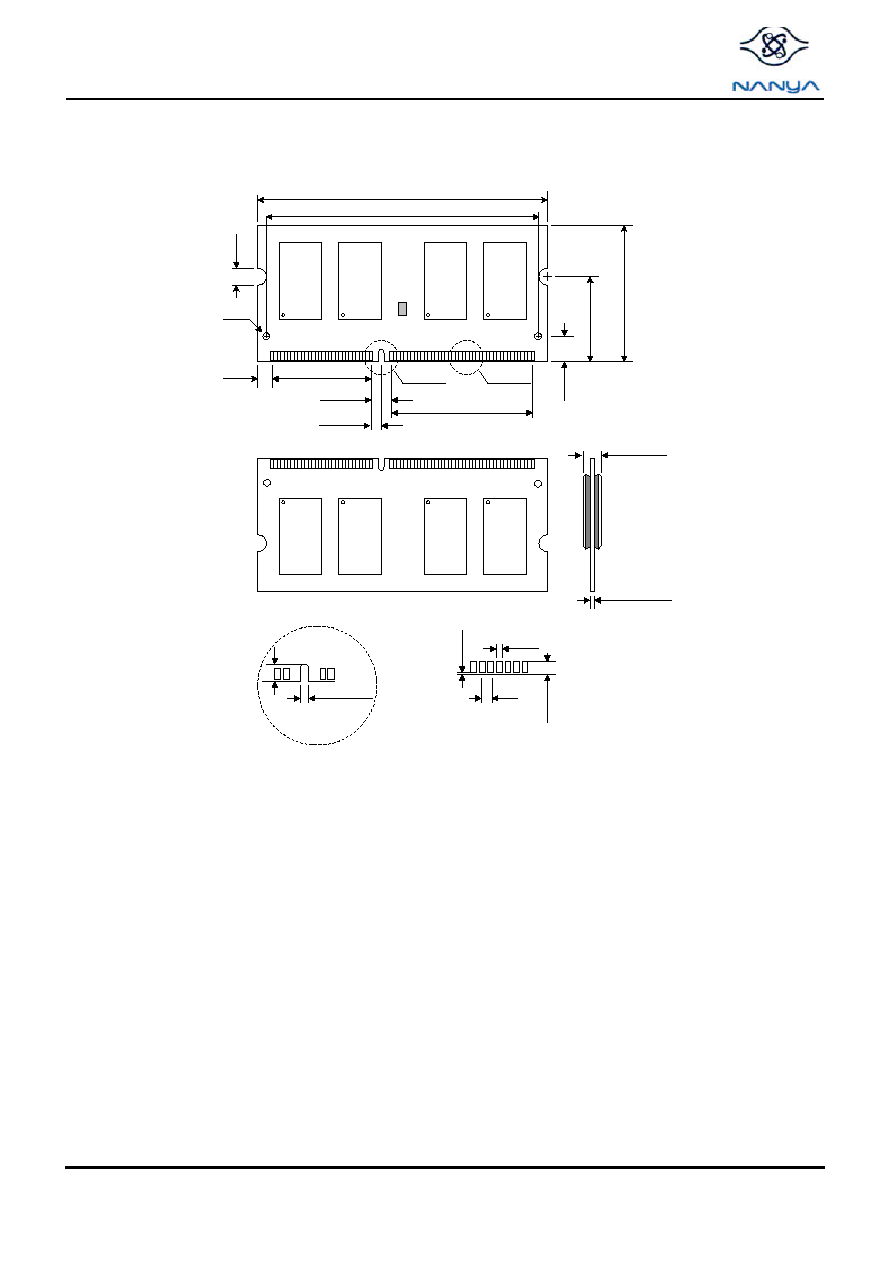
Package Dimensions
Note : All dimension are typical unless otherwise stated.
2.661
2.505
0.157+/-0.004
0.059+/- 0.004
FRONT
Side
0.039+/- 0.004
Detail A
0.100
0.031
Detail B
0.024
0.010 MAX
143
1
59 61
Detail A
Detail B
Unit : Inchs
0.157
0.787
1.250
0.236
0.130
0.913
0.181
0.098
1.291
0.150 MAX
2
60
62
144
(2X)
0.071