Document No. D15588EJ2V0DS00 (2nd edition)
Date Published April 2002 N CP(K)
Printed in Japan
SILICON POWER TRANSISTOR
2SA1649, 2SA1649-Z
PNP SILICON EPITAXIAL POWER TRANSISTOR
FOR HIGH-SPEED SWITCHING
DATA SHEET
The information in this document is subject to change without notice. Before using this document, please
confirm that this is the latest version.
Not all devices/types available in every country. Please check with local NEC representative for
availability and additional information.
©
2002
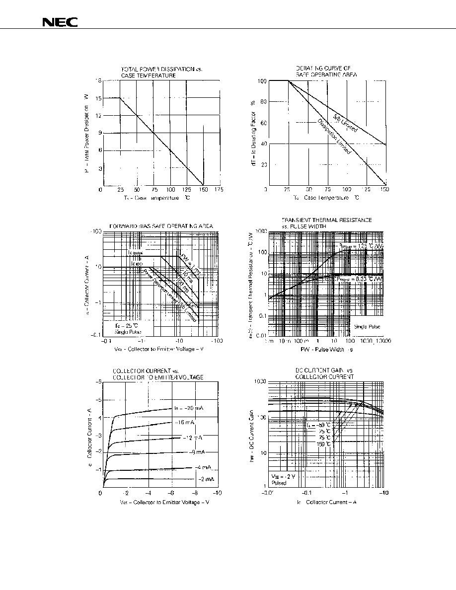
The 2SA1649 is a mold power transistor developed for high-
speed switching and features a very low collector-to-emitter
saturation voltage.
This transistor is ideal for use in switching regulators, DC/DC
converters, motor drivers, solenoid drivers, and other low-voltage
power supply devices, as well as for high-current switching.
FEATURES
∑ Available for high-current control in small dimension
∑ Z type is a lead processed product and is deal for mounting a
hybrid IC.
∑ Mold package that does not require an insulating board or
insulation bushing
∑ Low collector saturation voltage:
V
CE(sat)
=
-0.3 V MAX. (@I
C
=
-3 A)
∑ Fast switching speed:
t
f
= 0.3
µs MAX. (@I
C
=
-3 A)
∑ High DC current amplifiers and excellent linearity
ABSOLUTE MAXIMUM RATINGS (Ta = 25
∞
∞
∞
∞C)
Parameter
Symbol
Ratings
Unit
Collector to base voltage
V
CBO
-40
V
Collector to emitter voltage
V
CEO
-30
V
Emitter to base voltage
V
EBO
-7.0
V
Collector current (DC)
I
C(DC)
-10
A
Collector current (pulse)
I
C(pulse)
*
-20
A
Base current (DC)
I
B(DC)
-3.5
A
Total power dissipation
P
T
(Tc = 25
∞C)
15
W
Total power dissipation
P
T
(Ta = 25
∞C)
1.0**, 2.0***
W
Junction temperature
T
j
150
∞C
Storage temperature
T
stg
-55 to +150
∞C
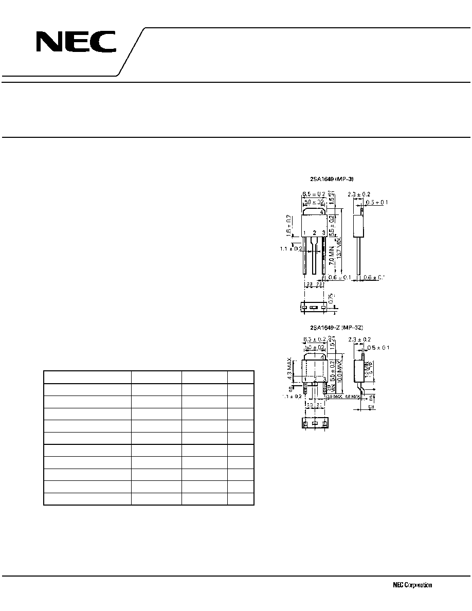
PACKAGE DRAWING (UNIT: mm)
(OHFWURGH &RQQHFWLRQ
%DVH
&ROOHFWRU
(PLWWHU
)LQ FROOHFWRU�
*:
PW
300
µs, duty cycle 10%
**: Printing board mounted
***: 7.5 mm
2
◊ 0.7 mm ceramic board mounted
Data Sheet D15588EJ2V0DS
2
2SA1649, 2SA1649-Z
ELECTRICAL CHARACTERISTICS (Ta = 25
∞
∞
∞
∞C)
Parameter
Symbol
Conditions
MIN.
TYP.
MAX.
Unit
Collector to emitter voltage
V
CEO(SUS)
I
C
=
-4.0 A, I
B
=
-0.4 A, L = 1 mH
-30
V
Collector to emitter voltage
V
CEX(SUS)
I
C
=
-4.0 A, I
B2
=
-I
B1
=
-0.4 A,
V
BE(OFF)
= 1.5 V, L = 180
µH, clamped
-40
V
Collector cutoff current
I
CBO
V
CE
=
-30 V, I
E
= 0
-10
µA
Collector cutoff current
I
CER
V
CE
=
-30 V, R
BE
= 50
, Ta = 125∞C
-1.0
mA
Collector cutoff current
I
CEX1
V
CE
=
-30 V, V
BE(OFF)
= 1.5 V
-10
µA
Collector cutoff current
I
CEX2
V
CE
=
-30 V, V
BE(OFF)
= 1.5 V,
Ta = 125
∞C
-1.0
mA
Emitter cutoff current
I
EBO
V
EB
=
-5.0 V, I
C
= 0
-10
µA
DC current gain
h
FE1
*
V
CE
=
-2.0 V, I
C
=
-0.5 A
100
-
DC current gain
h
FE2
*
V
CE
=
-2.0 V, I
C
=
-2.0 A
100
200
400
-
DC current gain
h
FE3
*
V
CE
=
-2.0 V, I
C
=
-4.0 A
60
-
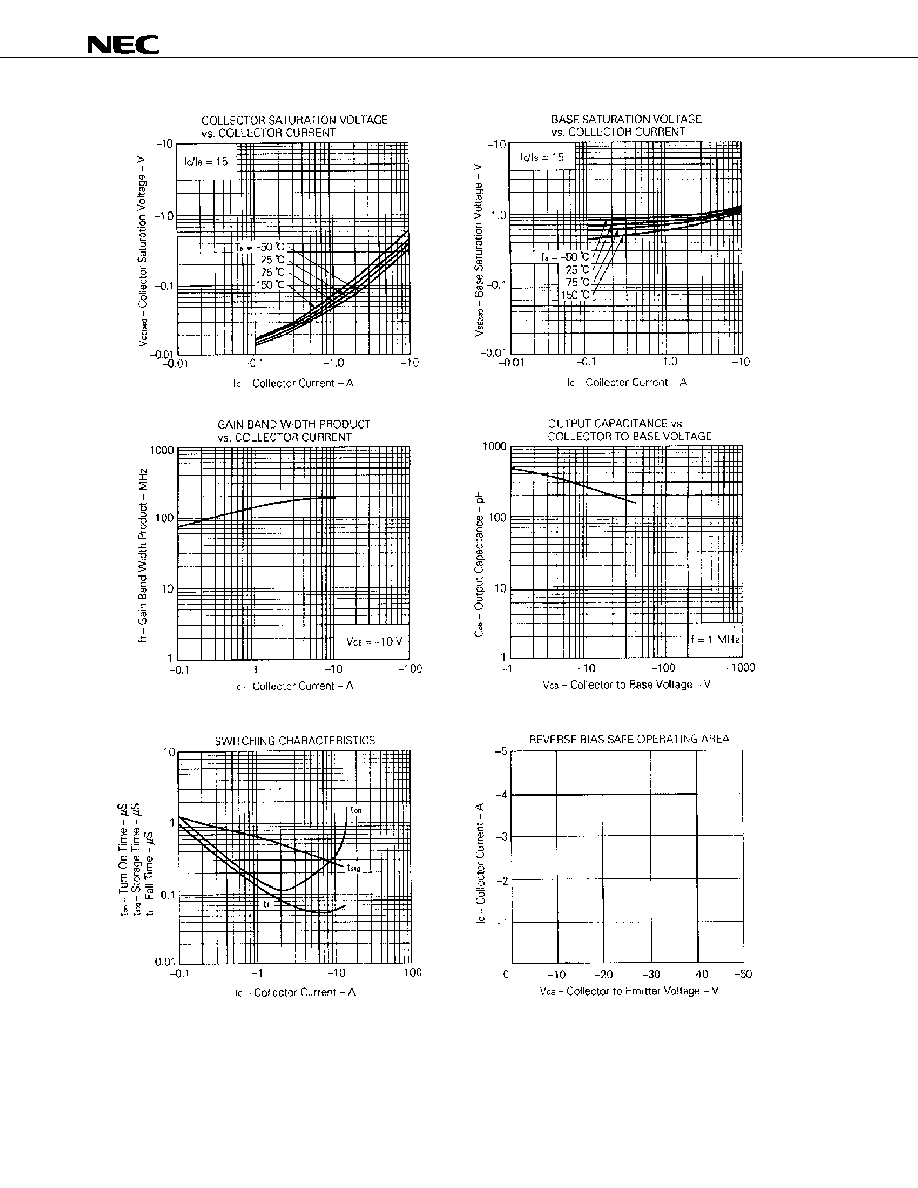
Collector saturation voltage
V
CE(sat)1
*
I
C
=
-3.0 A, I
B
=
-0.2 A
-0.3
V
Collector saturation voltage
V
CE(sat)2
*
I
C
=
-4.0 A, I
B
=
-0.3 A
-0.5
V
Base saturation voltage
V
BE(sat)1
*
I
C
=
-3.0 A, I
B
=
-0.2 A
-1.2
V
Base saturation voltage
V
BE(sat)2
*
I
C
=
-4.0 A, I
B
=
-0.3 A
-1.5
V
Collector capacitance
C
ob
V
CB
=
-10 V, I
E
= 0, f = 1.0 MHz
250
pF
Gain bandwidth product
f
T
V
CE
=
-10 V, I
C
=
-0.5 A
120
MHz
Turn-on time
t
on
0.3
µs
Storage time
t
stg
1.5
µs
Fall time
t
f
I
C
=
-4.0 A, R
L
= 5
,
I
B1
=
-I
B2
=
-0.15 A, V
CC
-20 V
Refer to the test circuit.
0.3
µs
* Pulse test PW
350
µs, duty cycle 2%/pulsed
h
)(
CLASSIFICATION
Marking
M
L
K
h
FE2
100 to 200
150 to 300
200 to 400
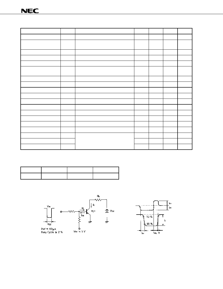
SWITCHING TIME (t
RQ
, t
VWJ
, t
I
) TEST CIRCUIT
%DVH FXUUHQW
ZDYHIRUP
&ROOHFWRU FXUUHQW
ZDYHIRUP