Document No. D14857EJ2V0DS00 (2nd edition)
Date Published April 2002 N CP(K)
Printed in Japan
DARLINGTON POWER TRANSISTOR
2SA1720
PNP SILICON EPITAXIAL TRANSISTOR (DARLINGTON CONNECTION)
FOR HIGH-SPEED SWITCHING
DATA SHEET
The information in this document is subject to change without notice. Before using this document, please
confirm that this is the latest version.
Not all devices/types available in every country. Please check with local NEC representative for
availability and additional information.
©
2002
The 2SA1720 is a high-speed Darlington power transistor.
This transistor is ideal for high-precision control such as PWM
control for pulse motors or brushless motors in OA and FA equipment.
FEATURES
∑ Mold package that does not require an insulating board or insulation
bushing
∑ On-chip C-to-E reverse diode
∑ Fast switching speed
ABSOLUTE MAXIMUM RATINGS (T
A
= 25
∞
∞
∞
∞C)
Parameter
Symbol
Conditions
Ratings
Unit
Collector to base voltage
V
CBO
-100
V
Collector to emitter voltage
V
CEO
-100
V
Emitter to base voltage
V
EBO
-8.0
V
Collector current (DC)
I
C(DC)
-10, +3.0
A
Collector current (pulse)
I
C(pulse)
PW
10 ms,
duty cycle
50%
≠
+20
A
Base current (DC)
I
B(DC)
-1.0
A
T
C
= 25
∞C
25
W
Total power dissipation
P
T
T
A
= 25
∞C
2.0
W
Junction temperature
T
j
150
∞C
Storage temperature
T
stg
-55 to +150
∞C
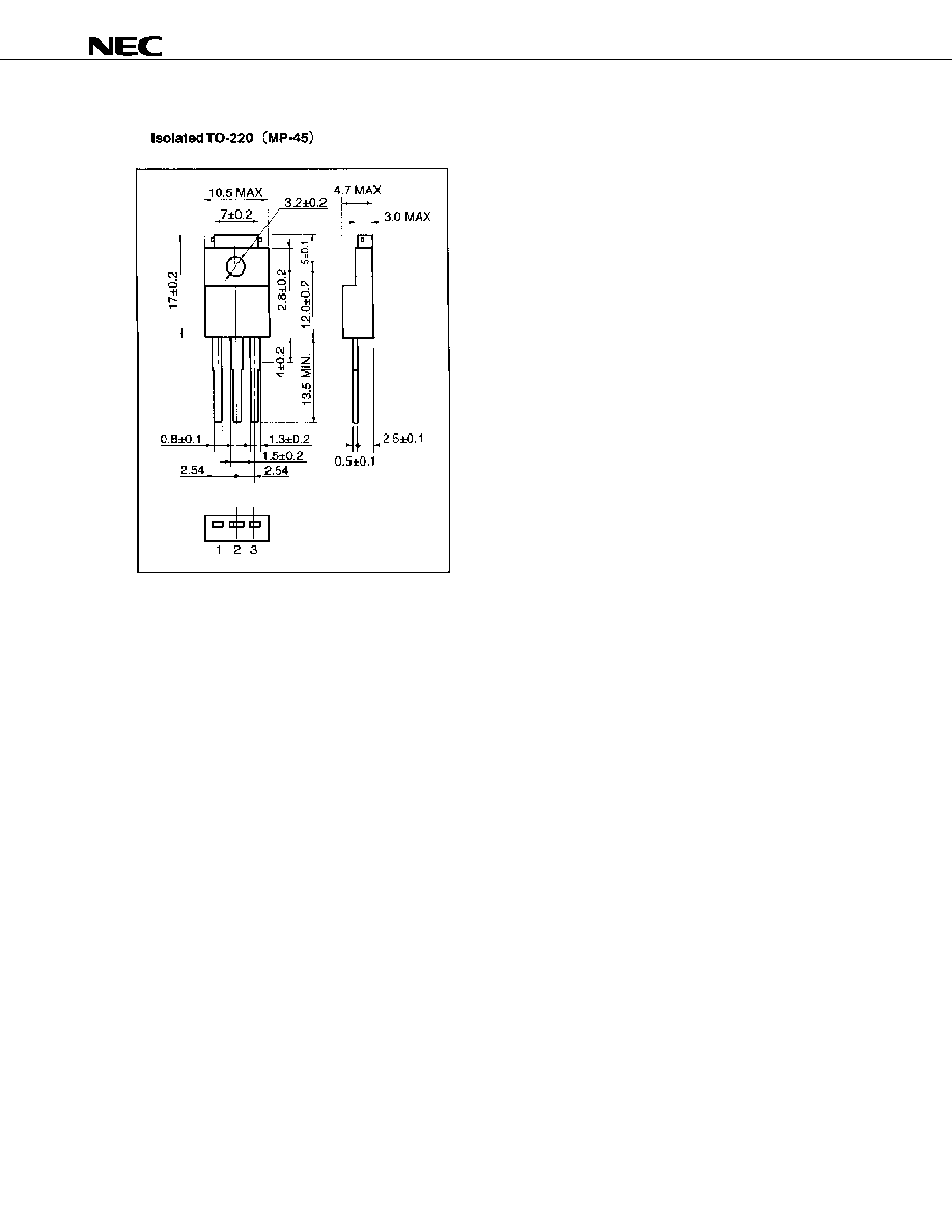
ORDERING INFORMATION
Part No.
Package
2SA1720
Isolated TO-220
EQUIVALENT CIRCUIT
1. Base
2. Collector
3. Emitter
Data Sheet D14857EJ2V0DS
2
2SA1720
ELECTRICAL CHARACTERISTICS (T
A
= 25
∞
∞
∞
∞C)
Parameter
Symbol
Conditions
MIN.
TYP.
MAX.
Unit
Collector cutoff current
I
CBO
V
CB
=
-100 V, I
E
= 0 A
-10
µA
DC current gain
h
FE1
V
CE
=
-2.0 V, I
C
=
-5.0 A
Note
4,000
20,000
DC current gain
h
FE2
V
CE
=
-2.0 V, I
C
=
-10 A
Note
500
Collector saturation voltage
V
CE(sat)
I
C
=
-5.0 A, I
B
=
-5.0 mA
Note
-0.9
-1.5
V
Base saturation voltage
V
BE(sat)
I
C
=
-5.0 A, I
B
=
-5.0 mA
Note
-1.5
-2.0
V
Gain bandwidth product
f
T
V
CE
=
-5.0 V, I
C
=
-5.0 A
100
MHz
Turn-on time
t
on
0.2
µs
Storage time
t
stg
1.5
µs
Fall time
t
f
I
C
= ≠5.0 A, R
L
= 10
,
I
B1
=
-I
B2
=
-5 mA, V
CC
-50 V
Refer to the switching time (t
on
, t
stg
, t
f
) test
circuit.
0.7
µs
1RWH Pulse test PW 350
µs, duty cycle 2%
h
FE
CLASSIFICATION
Marking
L
K
h
FE1
4,000 to 10,000
8,000 to 20,000
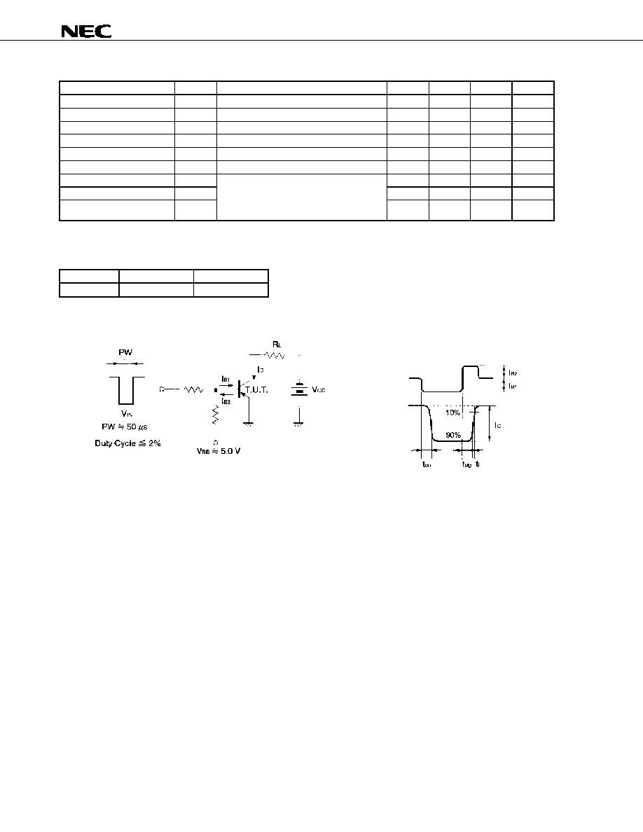
SWITCHING TIME (t
on
, t
stg
, t
f
) TEST CIRCUIT
%DVH FXUUHQW
ZDYHIRUP
&ROOHFWRU FXUUHQW
ZDYHIRUP

Data Sheet D14857EJ2V0DS
3
2SA1720
TYPICAL CHARACTERISTICS (T
A
= 25
∞
∞
∞
∞C)
7
R
WD
O
3
R
Z
H
U
'
L
VVLS
D
W
LR
Q
3
7
:�
&DVH 7HPSHUDWXUH 7
&
∞&�
&ROOHFWRU WR (PLWWHU 9ROWDJH 9
&(
9�
&DVH 7HPSHUDWXUH 7
&
∞&�
'
H
U
D
WLQ
J
G
7
�
&RO
O
H
F
W
RU
&
XUUHQW
,
&
$�
3XOVH :LGWK 3: PV�
&ROOHFWRU WR (PLWWHU 9ROWDJH 9
&(
9�
%DVH WR (PLWWHU 9ROWDJH 9
%(
9�
7UDQV
L
HQW
7
KHUPDO
5HV
L
V
W
DQ
F
H
U
WK
M
F
�
∞
&:�
&RO
O
H
F
W
RU
&
XUUHQW
,
&
$�
&RO
O
H
F
W
RU
&
XUUHQW
,
&
$�
6LQJOH SXOVH
3XOVH WHVW
3XOVH WHVW
6LQJOH SXOVH